 | ÐлекÑÑоннÑй компоненÑ: XR16L651 | СкаÑаÑÑ:  PDF PDF  ZIP ZIP |
/home/web/doc/html/exar/207982
Exar
Corporation 48720 Kato Road, Fremont CA, 94538
·
(510) 668-7000
·
FAX (510) 668-7017
·
www.exar.com
áç
áç
áç
áç
XR16L651
2.25V TO 5.5V UART WITH 32-BYTE FIFO
OCTOBER 2002
REV. 1.2.0
GENERAL DESCRIPTION
The XR16L651
1
(651) is a 2.25 to 5.5 volt Universal
Asynchronous Receiver and Transmitter (UART) with
5 volt tolerant inputs. This new device supports Intel
and Motorola data bus interface and is software
compatible to industry standard 16C450, 16C550,
ST16C580 and ST16C650A UARTs.
The 651 has 32 bytes of TX and RX FIFOs and is
capable of operating up to serial data rate of 3.125
Mbps at 5 volt supply voltage. The internal registers
include the 16C550 register set plus Exar's enhanced
registers for additional features to support today's
highly demanding data communication needs. The
enhanced features include automatic hardware and
software flow control, selectable TX and RX trigger
levels, and wireless infrared (IrDA) encoder/decoder.
The device provides a new capability to give user the
ability to program the wireless infrared encoder
output pulse width, hence, reduces the power
consumption of the handheld unit.
The XR16L651 device comes in a small 7x7x1mm
48-pin TQFP package with commercial and industrial
temperature ranges.
N
OTE
:
1 Covered by US patents #5,649,122 and #5,949,787
N
OTE
:
2 Underlined features are exclusive to XR16L651.
FEATURES
·
2.25 to 5.5 Volt Operation w/ 5 Volt Tolerant Inputs
·
ST16C450/550/580/650A Software Compatible
·
Intel, Motorola
2
or PC Mode 8-bit Bus Interface
·
Up to 3.125 Mbps Data Rate at 5 Volt Operation
·
32-byte Transmit and Receive FIFOs
·
Automatic RS485 Half-Duplex Control Output
·
Automatic Hardware (RTS/CTS) Flow Control
·
Hardware Flow Control Hysteresis
·
Automatic Software (Xon/Xoff) Flow Control
·
Infrared (IrDA) Encoder/Decoder Enable Input
2
·
Programmable Infrared Encoder Pulse Width
·
Sleep Mode with Wake-up Indicator via interrupt
·
48-pin TQFP Package (7x7x1mm)
·
Commercial and Industrial Temperature Grades
APPLICATIONS
·
Battery Operated Electronics
·
Internet Appliances
·
Handheld Terminal
·
Personal Digital Assistants
·
Cellular Phones DataPort
·
Wireless Infrared Data Communications Systems
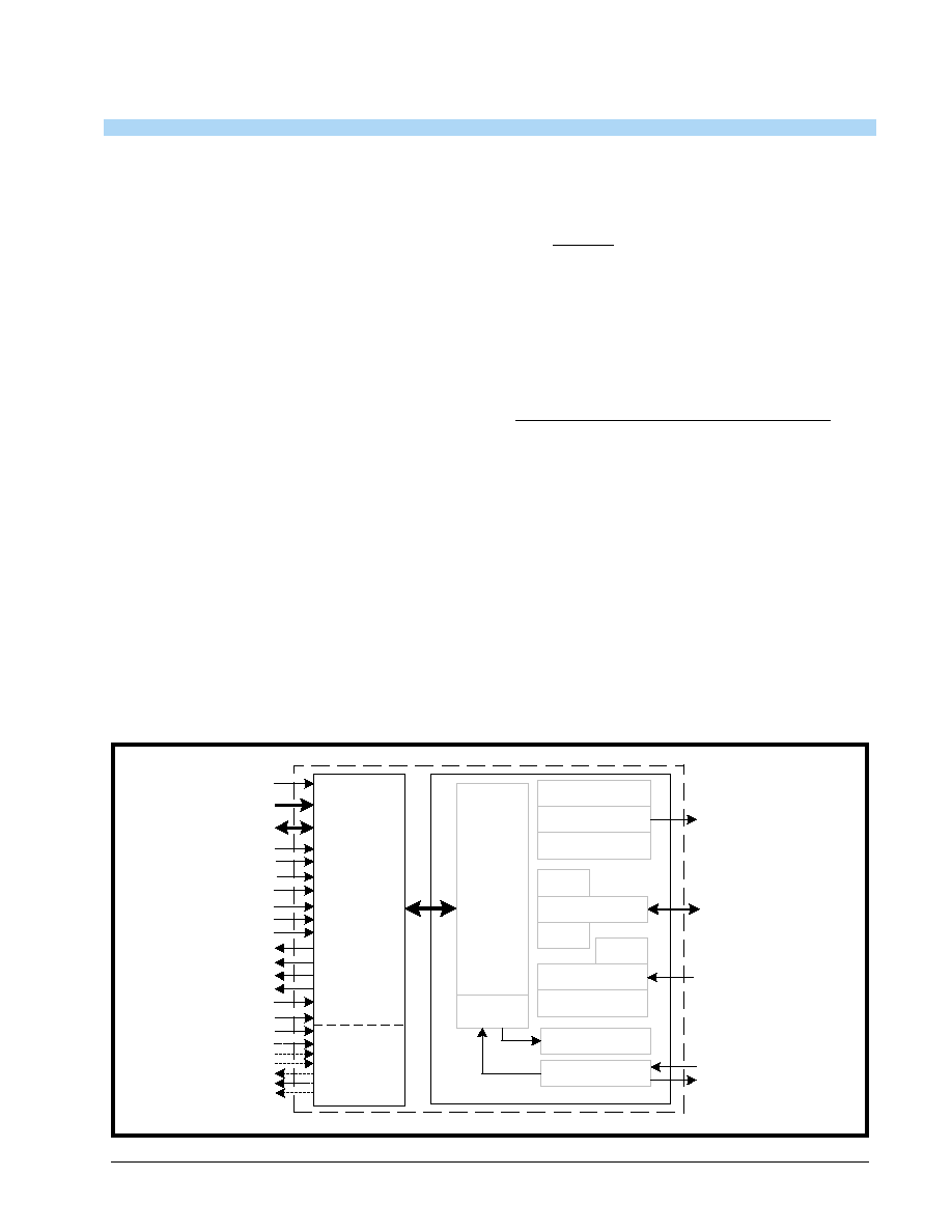
F
IGURE
1. B
LOCK
D
IAGRAM
XTAL1/CLK
XTAL2
Crystal Osc/Buffer
DTR#, DSR#,
RTS#, CTS#,
CD#, RI#
Intel,
Motorola
or PC
Data Bus
Interface
32 Byte TX FIFO
Baud Rate Generator
Infrared Encoder and
Pulse Width Control
Transmitter
UART
Configuration
Regs
IOR
IOR#
32 Byte RX FIFO
Infrared
Decoder
Receiver with Auto
Software Flow Control
Modem Control Signals
TX
RX
CTS Flow
Control
RTS Flow
Control
BRG
Prescaler
CS1
CS0
DDIS#
INT
TXRDY#
RDRDY#
A2:A0
D7:D0
IOW
CS2#
IM#
PCMODE#
S1
S2
S3
IRQA
IRQB
IRQC
IOW#/R/W#
RESET
PC Mode:
COM 1 to 4
Decode Logic
ENIR
áç
áç
áç
áç
XR16L651
2.25V TO 5.5V UART WITH 32-BYTE FIFO
REV. 1.2.0
2
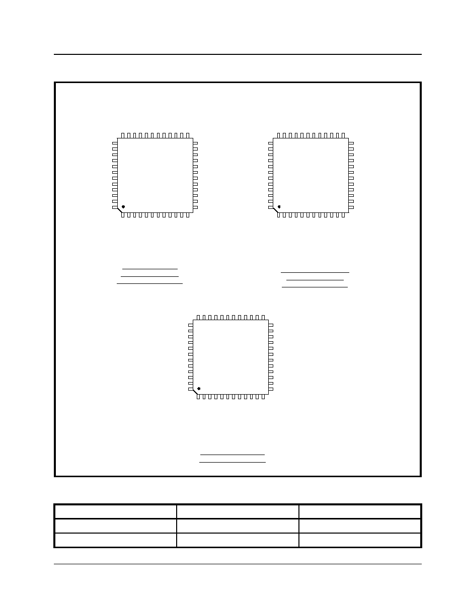
F
IGURE
2. I
NTEL
, M
OTOROLA
AND
PC
MODE
P
IN
O
UT
.
ORDERING INFORMATION
P
ART
N
UMBER
P
ACKAGE
O
PERATING
T
EMPERATURE
R
ANGE
XR16L651CM
48-TQFP
0°C to +70°C
XR16L651IM
48-TQFP
-40°C to +85°C
1 2 3 4 5 6 7 8 9 10 11 12
36 35 34 33 32 31 30 29 28 27 26 25
13
1
4
15
1
6
17
1
8
19 2
0
21 2
2
23 24
37
3
8
39
4
0
41
4
2
43 4
4
45 4
6
47 48
XR16L651
48-TQFP
in Intel Bus Mode
N.
C
.
D5
D6
D7
RL
C
K
A4
RX
TX
CS
0
CS
1
CS
2
#
B
A
UDOU
T
#
AS#
TXRDY#
DDIS#
S1
IOR
IOR#
GND
IOW
IOW#
XTAL2
XTAL1
ENIR
VC
C
R
ESET
OP
1
#
DT
R#
RT
S
#
OP
2
#
IN
T
RX
R
D
Y
#
A0
A1
A2
N.
C
GND
A9
CTS#
DSR#
CD#
RI#
VCC
D0
D1
D2
D3
D4
1 2 3 4 5 6 7 8 9 10 11 12
36 35 34 33 32 31 30 29 28 27 26 25
13
1
4
15
1
6
17
1
8
19 2
0
21 2
2
23 24
37
3
8
39
4
0
41
4
2
43 4
4
45 4
6
47 48
XR16L651
48-TQFP in
Motorola Bus Mode
N.
C
.
D5
D6
D7
RL
C
K
A4
RX
TX
CS
0
CS
1
CS
2
#
B
A
UDOU
T
#
AS#
TXRDY#
DDIS#
S1
GND
GND
GND
GND
R/W#
XTAL2
XTAL1
ENIR
VC
C
R
ESET
#
OP
1
#
DT
R#
RT
S
#
OP
2
#
IN
T#
RX
R
D
Y
#
A0
A1
A2
N.
C
VCC
A9
CTS#
DSR#
CD#
RI#
VCC
D0
D1
D2
D3
D4
1 2 3 4 5 6 7 8 9 10 11 12
36 35 34 33 32 31 30 29 28 27 26 25
13
1
4
15
1
6
17
1
8
19 2
0
21 2
2
23 24
37
3
8
39
4
0
41
4
2
43 4
4
45 4
6
47 48
XR16L651
48-TQFP
in PC Mode
N.
C
.
D5
D6
D7
S2
A4
RX
TX
A5
A6
A7
LPT1#
AEN#
IRQC
LPT2#
S1
A3
IOR#
GND
A8
IOW#
XTAL2
XTAL1
ENIR
GND
R
ESET
OP
1
#
DT
R#
RT
S
#
S3
IR
Q
A
IR
Q
B
A0
A1
A2
N.
C
GND
A9
CTS#
DSR#
CD#
RI#
VCC
D0
D1
D2
D3
D4
Intel Bus Mode with
IM# tied to GND and
PCMODE# tied to VCC
Motorola Bus Mode with
IM# tied to VCC and
PCMODE# tied to VCC
PC Mode with IM# and
PCMODE# tied to GND
IM#
: PIN 37
PCMODE#
: PIN 36

XR16L651
áç
áç
áç
áç
2.25V TO 5.5V UART WITH 32-BYTE FIFO
REV. 1.2.0
3
PIN DESCRIPTIONS
N
AME
P
IN
#
T
YPE
D
ESCRIPTION
16 (Intel) or 68 (Motorola) MODE DATA BUS INTERFACE. The PCMODE# pin is connected to VCC.
A2
A1
A0
26
27
28
I
Address data lines [2:0]
A2:A0 selects internal UART's configuration registers.
D7
D6
D5
D4
D3
D2
D1
D0
4
3
2
48
47
46
45
44
IO
Data bus lines [7:0] (bidirectional)
IOR#
19
I
Input/Output Read (active low)
When IM# pin is at logic 0, it selects Intel bus interface and this input is read
strobe (active low). The falling edge instigates an internal read cycle and
retrieves the data byte from an internal register pointed by the address lines
[A2:A0], places it on the data bus to allow the host processor to read it on the
leading edge. When IM# pin is at logic 1, it selects Motorola bus interface and
the IOR# input is not used and it should be connected to GND to minimize
supply current. Its function is the same as IOR, except it is active low. Either
an active IOR# or IOR is required to transfer data from 651 to CPU during a
read operation. If this input is unused in the Intel bus mode (IM# pin is at logic
0), it should be connected to VCC to minimize supply current.
IOR
20
I
Input/Output Read (active high)
Same as IOR# but active high. When IM# pin is at logic 1 for Motorola bus
mode, this pin is not used and should be connected to GND to minimize sup-
ply current. If this input is unused in the Intel bus mode (IM# pin is at logic 0),
it should be connected to GND to minimize supply current.
IOW#
(R/W#)
16
I
When IM# pin is at logic 0, it selects Intel bus interface and this input
becomes write strobe (active low). The falling edge instigates the internal
write cycle and the trailing edge transfers the data byte on the data bus to an
internal register pointed by the address lines [A2:A0]. Its function is the same
as IOW, except it is active low. Either an active IOW# or IOW is required to
transfer data from 651 to the Intel type CPU during a write operation. When
IM# pin is at logic 1, it selects Motorola bus interface and this input becomes
R/W# signal for read (logic 1) and write (logic 0). If this input is unused in the
Intel bus mode (IM# pin is at logic 0), it should be connected to VCC to mini-
mize supply current.
IOW
17
I
Input/Output Write (active high)
Same as IOW# but active high. When IM# pin is at logic 1 for Motorola bus
mode, this pin must be connected to GND to allow IOW# input to function cor-
rectly. If this input is unused in the Intel bus mode (IM# pin is at logic 0), it
should be connected to GND to minimize supply current.
CS0
9
I
Chip Select 0 input (active high)
This input selects the XR16L651 device. If CS1 or CS2# is used as the chip
select then this pin must be connected to VCC. The 651 is selected when all
three chip selects are active. See
Figure 3
through
Figure 5
.

áç
áç
áç
áç
XR16L651
2.25V TO 5.5V UART WITH 32-BYTE FIFO
REV. 1.2.0
4
CS1
10
I
Chip Select 1 input (active high)
This input selects the XR16L651 device. If CS0 or CS2# is used as the chip
select then this pin must be connected to VCC. The 651 is selected when all
three chip selects are active. See
Figure 3
through
Figure 5
.
CS2#
11
I
Chip Select 2 input (active low)
This input selects the XR16L651 device. If CS0 or CS1 is used as the chip
select then this pin must be connected to GND. The 651 is selected when all
three chip selects are active. See
Figure 3
through
Figure 5
.
INT
(INT#)
30
O
Interrupt Output
This output becomes active whenever the transmitter, receiver, line and/or
modem status register has an active condition. See interrupt section for more
detail. When IM# pin is at logic 0 (Intel bus mode), this interrupt output may
be set to normal active high or active high open source to provide wire-OR
capability by connecting a 1k to 10k ohms resistor between this pin and
ground. When IM# pin is at logic 1 (Motorola bus mode), this interrupt output
becomes an open drain, active low output. It requires an external pull-up
resistor of 1K-10K ohms to operate properly. The output may be wire-OR'ed
with other devices in the system to form a single interrupt request to the host
processor and have the software driver poll all devices to determine the inter-
rupting condition(s).
AS#
24
I
Address Strobe input (active low)
In the Intel bus mode, the leading-edge transition of AS# latches the chip
selects (CS0, CS1, CS2#) and the address lines A0, A1 and A2. This input is
used when the address lines and chip select inputs are not stable for the
duration of a read or write operation, i.e.,for a processor that needs to de-mul-
tiplex the address and data lines. If not required, this input can be perma-
nently tied to GND. This input is not used in the Motorola mode.
TXRDY#
23
O
UART Transmitter Ready (active low)
The output provides the TX FIFO/THR status. See
Table 2
. If it is not used,
leave it unconnected.
RXRDY#
29
O
UART Receiver Ready (active low)
This output provides the RX FIFO/RHR status for receive channel A. See
Table 2
. If it is not used, leave it unconnected.
PC Mode Interface Signals. Connect PCMODE# pin to GND and IM# pin to GND to select PC Mode.
A3
A4
A5
A6
A7
A8
A9
20
6
9
10
11
17
38
I
PC mode additional Address Lines
In the PC mode, these are the additional address lines from the host address
bus. They are inputs to the on-board chip select decode function for COM 1-4
and LPT ports. See
Table 1
for details. The pins A4 and A9 have internal
100k
pull-up resistors.
AEN#
24
I
Address Enable input (active low)
When AEN# transition to logic 0, it decodes and validates COM 1-4 ports
address per S1, S2 and S3 inputs.
N
AME
P
IN
#
T
YPE
D
ESCRIPTION
XR16L651
áç
áç
áç
áç
2.25V TO 5.5V UART WITH 32-BYTE FIFO
REV. 1.2.0
5
S1
S2
S3
21
5
31
I
Select 1 to 3
These are the standard PC COM 1-4 ports and IRQ selection inputs. See
Table 1
and
Table 3
for details. The S1 pin has an internal 100k
pull-up
resistor.
IRQA
IRQB
IRQC
30
29
23
O
Interrupt Request A, B and C Outputs (active high, tri-state)
These are the interrupt outputs associated with COM 1-4 to be connected to
the host data bus. See interrupt section for details. The Interrupt Requests A,
B or C functions as IRQx to the PC bus. IRQx is enabled by setting MCR bit-3
to logic 1 and the desired interrupt(s) in the interrupt enable register (IER).
LPT1#
12
O
Line Printer Port-1 Decode Logic Output (active low)
This pin functions as the PC standard LPT-1 printer port address decode logic
output, see
Table 1
. The baud rate generator clock output, BAUDOUT#, is
internally connected to the RCLK input in the PC mode.
LPT2#
22
O
Line Printer Port-2 Decode Logic Output (active low)
This pin functions as the PC standard LPT-2 printer port address decode logic
output, see
Table 1
.
MODEM OR SERIAL I/O INTERFACE
TX
8
O
Transmit Data or wireless infrared transmit data
This output is active low in normal standard serial interface operation (RS-
232, RS-422 or RS-485) and active high in the infrared mode. Infrared mode
can be enabled by connecting pin ENIR to VCC or through software settling
after power up.
RX
7
I
Receive Data or wireless infrared receive data
Normal received data input idles at logic 1 condition and logic 0 in the infrared
mode. The wireless infrared pulses are applied to the decoder. This input
must be connected to its idle logic state in either normal, logic 1, or infrared
mode, logic 0, else the receiver may report "receive break" and/or "error" con-
dition(s).
RTS#
32
O
Request to Send or general purpose output (active low)
This port may be used for one of two functions:
1) automatic hardware flow control, see EFR bit-6, MCR bit-1and IER bit-6.
2) RS485 half-duplex direction control, see XFR bits 2 and 5.
RTS# output must be asserted before auto RTS flow control can start.
CTS#
39
I
Clear to Send or general purpose input (active low)
If used for automatic hardware flow control, data transmission will be stopped
when this pin is de-asserted and will resume when this pin is asserted again.
See EFR bit-7 and IER bit-7.
DTR#
33
O
Data Terminal Ready or general purpose output (active low).
DSR#
40
I
Data Set Ready input or general purpose input (active low).
CD#
41
I
Carrier Detect input or general purpose input (active low).
RI#
42
I
Ring Indicator input or general purpose input (active low).
ANCILLARY SIGNALS
XTAL1
14
I
Crystal or external clock input. Caution: this input is not 5V tolerant.
XTAL2
15
O
Crystal or buffered clock output.
N
AME
P
IN
#
T
YPE
D
ESCRIPTION
Document Outline