Exar
Corporation 48720 Kato Road, Fremont CA, 94538
�
(510) 668-7000
�
FAX (510) 668-7017
�
www.exar.com
��
��
��
��
XR16L2550
LOW VOLTAGE DUART WITH 16-BYTE FIFO
SEPTEMBER 2003
REV. 1.0.0
GENERAL DESCRIPTION
The XR16L2550
1
(L2550) is a dual universal
asynchronous receiver and transmitter (UART). The
XR16L2550 is an improved version of the
ST16C2550 UART with lower operating voltages and
5 volt tolerant inputs. The L2550 provides enhanced
UART functions with 16 byte FIFOs, a modem control
interface and data rates up to 4 Mbps. Onboard
status registers provide the user with error indications
and operational status. System interrupts and modem
control features may be tailored by external software
to meet specific user requirements. Independent
programmable baud rate generators are provided to
select transmit and receive clock rates up to 3.125
Mbps. The Baud Rate Generator can be configured
for either crystal or external clock input. An internal
loopback capability allows onboard diagnostics. The
L2550 is available in a 44-pin PLCC, 48-pin TQFP
and 32-pin QFN packages. The L2550 is fabricated in
an advanced CMOS process.
N
OTE
:
1 Covered by U.S. Patent #5,649,122.
APPLICATIONS
�
Portable Appliances
�
Medical Monitors
�
Base Stations
�
Micro Servers
�
Telecommunication Network Routers
�
Industrial Automation Controls
FEATURES
�
2.25 to 5.5 Volt operation
�
5 Volt tolerant inputs
�
Pin-to-pin compatible to Exar's ST16C2450,
ST16C2550 and XR16L2750 in 44-PLCC and 48-
TQFP packages
�
Pin-to-pin compatible to XR16C2850 in 44-PLCC
�
Pin alike XR16L2551, XR16L2751 and XR16C2850
in 48-TQFP package
�
Two independent UART channels
s
Up to 3.125Mbps with external clock of 50 MHz
s
Register Set compatible to 16C550
s
16 byte Transmit FIFO to reduce the bandwidth
requirement of the external CPU
s
16 byte Receive FIFO with error tags to reduce
the bandwidth requirement of the external CPU
s
4 selectable Receive FIFO interrupt trigger
levels
s
Automatic RTS/CTS hardware flow control
s
Automatic Xon/Xoff software flow control
s
Wireless infrared encoder/decoder
s
Full Modem Interface (CTS#, RTS#, DSR#,
DTR#, RI#, CD#)
s
Programmable character lengths (5, 6, 7, 8)
with even, odd, or no parity
�
Tiny 32-QFN, no lead package (5x5x0.9mm)
�
44-PLCC and 48-TQFP packages also available
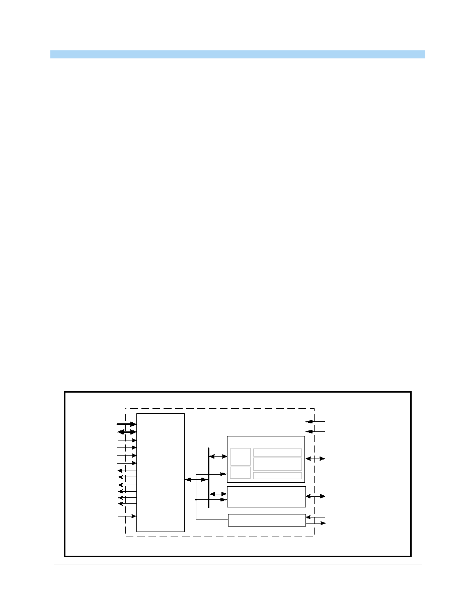
F
IGURE
1. XR16L2550 B
LOCK
D
IAGRAM
XTAL1
XTAL2
Crystal Osc/Buffer
TXA, RXA, DTRA#,
DSRA#, RTSA#,
DTSA#, CDA#, RIA#,
OP2A#
8-bit Data
Bus
Interface
UART Channel A
16 Byte TX FIFO
16 Byte RX FIFO
BRG
TX & RX
UART
Regs
2.25 to 5.5 Volt VCC
GND
TXB, RXB, DTRB#,
DSRB#, RTSB#,
CTSB#, CDB#, RIB#,
OP2B#
UART Channel B
(same as Channel A)
A2:A0
D7:D0
CSA#
CSB#
INTA
INTB
IOW#
IOR#
Reset
TXRDYA#
TXRDYB#
RXRDYA#
RDRXYB#
* 5 Volt Tolerant Inputs

��
��
��
��
XR16L2550
REV. 1.0.0
LOW VOLTAGE DUART WITH 16-BYTE FIFO
3
PIN DESCRIPTIONS
Pin Description
N
AME
32-QFN
P
IN
#
44-PLCC
P
IN
#
48-TQFP
P
IN
#
T
YPE
D
ESCRIPTION
DATA BUS INTERFACE
A2
A1
A0
18
19
20
29
30
31
26
27
28
I
Address data lines [2:0]. These 3 address lines select
one of the internal registers in UART channel A/B during
a data bus transaction.
D7
D6
D5
D4
D3
D2
D1
D0
2
1
32
31
30
29
28
27
9
8
7
6
5
4
3
2
3
2
1
48
47
46
45
44
IO
Data bus lines [7:0] (bidirectional).
IOR#
14
24
19
I
Input/Output Read Strobe (active low). The falling edge
instigates an internal read cycle and retrieves the data
byte from an internal register pointed to by the address
lines [A2:A0]. The data byte is placed on the data bus to
allow the host processor to read it on the rising edge.
IOW#
12
20
15
I
Input/Output Write Strobe (active low). The falling edge
instigates an internal write cycle and the rising edge
transfers the data byte on the data bus to an internal reg-
ister pointed by the address lines.
CSA#
7
16
10
I
UART channel A select (active low) to enable UART chan-
nel A in the device for data bus operation.
CSB#
8
17
11
I
UART channel B select (active low) to enable UART chan-
nel B in the device for data bus operation.
INTA
22
33
30
O
UART channel A Interrupt output. The output state is
defined by the user and through the software setting of
MCR[3]. INTA is set to the active mode (active high) and
OP2A# output to a logic 0 when MCR[3] is set to a logic
1. INTA is set to the three state mode and OP2A# to a
logic 1 when MCR[3] is set to a logic 0 (Default).
INTB
21
32
29
O
UART channel B Interrupt output. The output state is
defined by the user and through the software setting of
MCR[3]. INTB is set to the active mode and OP2B# out-
put to a logic 0 when MCR[3] is set to a logic 1. INTB is
set to the three state mode and OP2B# to a logic 1 when
MCR[3] is set to a logic 0 (Default).
TXRDYA#
-
1
43
O
UART channel A Transmitter Ready (active low). The
output provides the TX FIFO/THR status for transmit
channel A. If it is not used, leave it unconnected.
RXRDYA#
-
34
31
O
UART channel A Receiver Ready (active low). This output
provides the RX FIFO/RHR status for receive channel A.
If it is not used, leave it unconnected.

XR16L2550
��
��
��
��
LOW VOLTAGE DUART WITH 16-BYTE FIFO
REV. 1.0.0
4
TXRDYB#
-
12
6
O
UART channel B Transmitter Ready (active low). The out-
put provides the TX FIFO/THR status for transmit channel
B. If it is not used, leave it unconnected.
RXRDYB#
-
23
18
O
UART channel B Receiver Ready (active low). This output
provides the RX FIFO/RHR status for receive channel B.
If it is not used, leave it unconnected.
MODEM OR SERIAL I/O INTERFACE
TXA
5
13
7
O
UART channel A Transmit Data. If it is not used, leave it
unconnected.
RXA
4
11
5
I
UART channel A Receive Data. Normal receive data input
must idle at logic 1 condition. If it is not used, tie it to VCC
or pull it high via a 100k ohm resistor.
RTSA#
23
36
33
O
UART channel A Request-to-Send (active low) or general
purpose output. This output must be asserted prior to
using auto RTS flow control, see EFR[6], MCR[1] and
IER[6]. If it is not used, leave it unconnected.
CTSA#
25
40
38
I
UART channel A Clear-to-Send (active low) or general
purpose input. It can be used for auto CTS flow control,
see EFR[7] and IER[7]. This input should be connected to
VCC when not used.
DTRA#
-
37
34
O
UART channel A Data-Terminal-Ready (active low) or
general purpose output. If it is not used, leave it uncon-
nected.
DSRA#
-
41
39
I
UART channel A Data-Set-Ready (active low) or general
purpose input. This input should be connected to VCC
when not used. This input has no effect on the UART.
CDA#
-
42
40
I
UART channel A Carrier-Detect (active low) or general
purpose input. This input should be connected to VCC
when not used. This input has no effect on the UART.
RIA#
-
43
41
I
UART channel A Ring-Indicator (active low) or general
purpose input. This input should be connected to VCC
when not used. This input has no effect on the UART.
OP2A#
-
35
32
O
Output Port 2 Channel A - The output state is defined by
the user and through the software setting of MCR[3].
INTA is set to the active mode and OP2A# output to a
logic 0 when MCR[3] is set to a logic 1. INTA is set to the
three state mode and OP2A# to a logic 1 when MCR[3] is
set to a logic 0. This output should not be used as a gen-
eral output else it will disturb the INTA output functionality.
If it is not used at all, leave it unconnected.
TXB
6
14
8
O
UART channel B Transmit Data. If it is not used, leave it
unconnected.
RXB
3
10
4
I
UART channel B Receive Data. Normal receive data input
must idle at logic 1 condition. If it is not used, tie it to VCC
or pull it high via a 100k ohm resistor.
Pin Description
N
AME
32-QFN
P
IN
#
44-PLCC
P
IN
#
48-TQFP
P
IN
#
T
YPE
D
ESCRIPTION

��
��
��
��
XR16L2550
REV. 1.0.0
LOW VOLTAGE DUART WITH 16-BYTE FIFO
5
Pin type: I=Input, O=Output, IO= Input/output, OD=Output Open Drain.
1.0
PRODUCT DESCRIPTION
The XR16L2550 (L2550) provides serial asynchronous receive data synchronization, parallel-to-serial and
serial-to-parallel data conversions for both the transmitter and receiver sections. These functions are
RTSB#
15
27
22
O
UART channel B Request-to-Send (active low) or general
purpose output. This output must be asserted prior to
using auto RTS flow control, see EFR[6], MCR[1] and
IER[6]. If it is not used, leave it unconnected.
CTSB#
16
28
23
I
UART channel B Clear-to-Send (active low) or general
purpose input. It can be used for auto CTS flow control,
see EFR[7] and IER[7]. This input should be connected to
VCC when not used.
DTRB#
-
38
35
O
UART channel B Data-Terminal-Ready (active low) or
general purpose output. If it is not used, leave it uncon-
nected.
DSRB#
-
25
20
I
UART channel B Data-Set-Ready (active low) or general
purpose input. This input should be connected to VCC
when not used. This input has no effect on the UART.
CDB#
-
21
16
I
UART channel B Carrier-Detect (active low) or general
purpose input. This input should be connected to VCC
when not used. This input has no effect on the UART.
RIB#
-
26
21
I
UART channel B Ring-Indicator (active low) or general
purpose input. This input should be connected to VCC
when not used. This input has no effect on the UART.
OP2B#
-
15
9
O
Output Port 2 Channel B - The output state is defined by
the user and through the software setting of MCR[3].
INTB is set to the active mode and OP2B# output to a
logic 0 when MCR[3] is set to a logic 1. INTB is set to the
three state mode and OP2B# to a logic 1 when MCR[3] is
set to a logic 0. This output should not be used as a gen-
eral output else it will disturb the INTB output functionality.
If it is not used, leave it unconnected.
ANCILLARY SIGNALS
XTAL1
10
18
13
I
Crystal or external clock input.
XTAL2
11
19
14
O
Crystal or buffered clock output.
RESET
24
39
36
I
Reset (active high) - A longer than 40 ns logic 1 pulse on
this pin will reset the internal registers and all outputs.
The UART transmitter output will be held at logic 1, the
receiver input will be ignored and outputs are reset during
reset period.
VCC
26
44
42
Pwr
2.25V to 5.5V power supply. All inputs are 5V tolerant.
GND
13
22
17
Pwr
Power supply common, ground.
N.C.
9, 17
-
12, 24, 25,
37
No Connection. These pins are open, but typically, should
be connected to GND for good design practice.
Pin Description
N
AME
32-QFN
P
IN
#
44-PLCC
P
IN
#
48-TQFP
P
IN
#
T
YPE
D
ESCRIPTION
