 | ÐлекÑÑоннÑй компоненÑ: VP-1608 | СкаÑаÑÑ:  PDF PDF  ZIP ZIP |
þÿ
VOICE
Eletech Electronics, Inc.
16019 Kaplan Avenue
Industry, CA 91744, U.S.A.
Tel: (626) 333-6394 Fax: (626) 333-6494
Eletech Enterprise Co., Ltd.
531-3F Chung-Cheng Road
Hsin Tien, Taipei Hsien, Taiwan
Tel:+886 2-2218-0068 Fax:+886 2-2218-0254
http://www.eletech.com
FEATURES
n Plays messages stored in external EPROM chips
n CVSD technique with adjustable sampling rate from
16K to 128K bps for different voice quality
n Dual-channel audio output
n Up to 64 segments per channel
n Built-in RC oscillator or use external clock
GENERAL DESCRIPTIONS
The VP-1608 is a CMOS LSI speech processor chip based
on the CVSD (Continuously Variable Slope Delta) modula-
tion technique. The VP-1608 not only combines the func-
tions of the VP1000 and the VP1600 together, but also
provides extended direct EPROM addressing (up to 8M
bits) and dual-channel audio output.
Note that although the dual-channel output provided by
the VP1608 can be used as a stereo output, it will be hard
to do so since the VP-880 Voice Development System does
not allow stereo voice digitization.
VP-1608
Digital Voice Processor
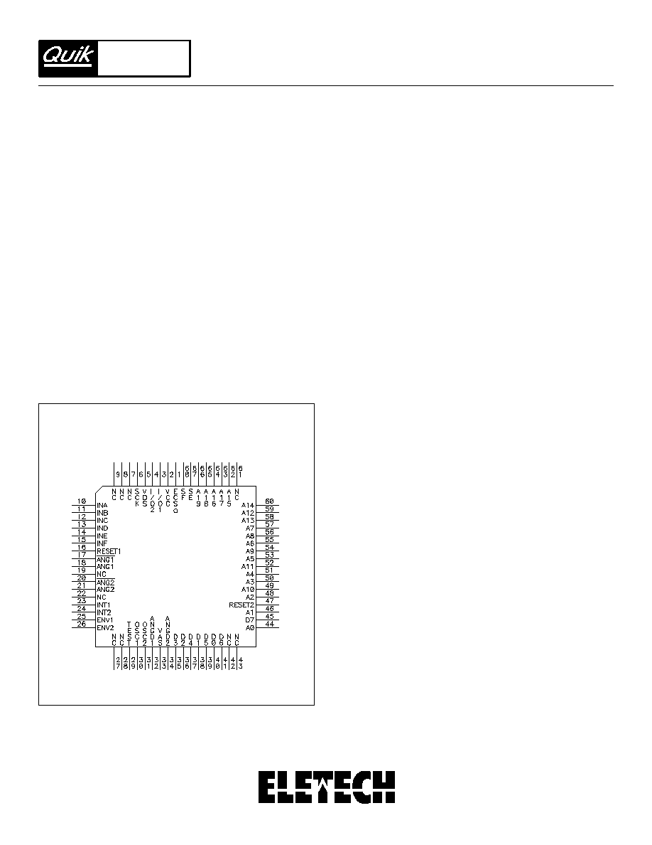
VP-1608 (PLCC68) Pin Assignment
n Direct EPROM addressing up to 8M bits
n Low power, single voltage operation
n Microprocessor interface
n Low-cost VP-880 system available for quick and easy
voice development
Therefore the dual-channel output is usually used in appli-
cations where sound synchronization is not critical. For
example, in a game equipment, channel A can be playing
a continuous background sound when channel B plays
short sound effects based on the player's action.
The dual-channel output is available on two separate
output pins. They can be used independently, or mixed
together externally. Each channel may control up to 64
sound segments stored in 4 different EPROM banks, with
up to 16 segments in each bank.
Each segment stored in the EPROM is represented by a
unique binary code: 2 bits for the bank code and 4 bits for
the segment code. A valid code plus a strobe signal are all
it takes to activate a certain segment.
The VP-1608 can operate in a wide range of sampling rates
(from 16 to 128 Kbps). A higher sampling rate usually
produces better sound quality at the expense of higher
memory cost. As a rule of thumb, start with 32 Kbps. A 1M
EPROM can store 32 seconds of sound at this rate.
Thanks to the chip's high internal integration, very little
external components are required to build a VP-1608
based design. The VP880 Voice Development System is
available for quick and easy in-house voice development.
APPLICATIONS
n Dual channel, multiple message playback
n Sound effects generator
n Digital announcer for consumer, industrial, security
and telecommunication products

ABSOLUTE MAXIMUM RATINGS*
Supply Voltage, V
CC
- V
DS
.................................. 0 to 5.5V
Input Volotage, V
IN
........................................... V
DS
to V
CC
Operating Temperature, T
OP
...................... -10
o
C to 60
o
C
Storage Temperature, T
ST
.......................... -20
o
C to 80
o
C
* Stresses above those listed under "Absolute Maximum
Ratings" may cause permanent damage to the device. This
is a stress rating only and functional operation of the
device at these or any other conditions above those
indicated in the operational sections of this specification
is not implied.
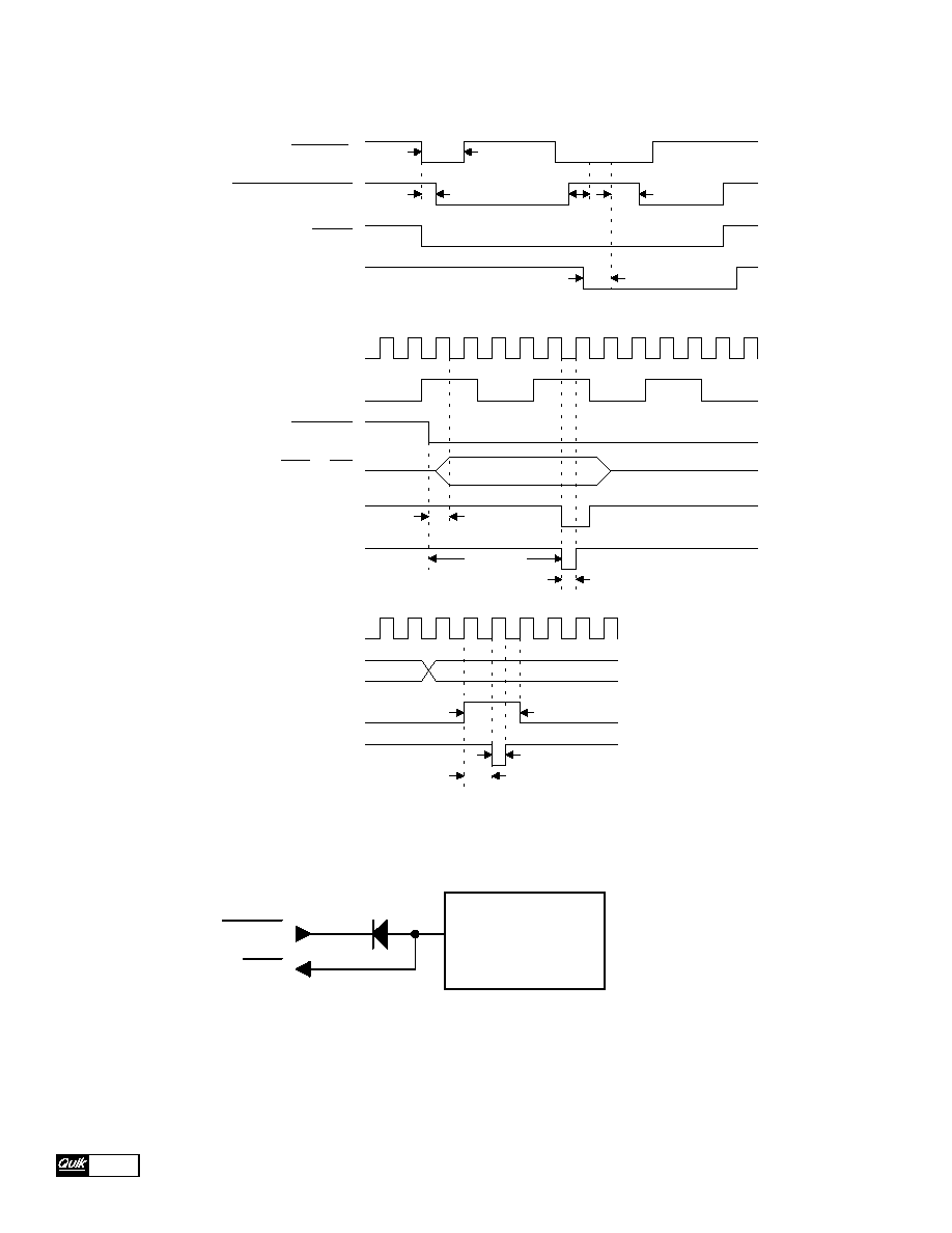
ELECTRICAL CHARACTERISTICS
Symbol
Parameter
Min.
Typ.
Max.
Units
V
CC
Supply Voltage
4.5
5
5.5
V
I
DD
Standby Current
50
uA
I
DRIVE
Output Current V
OH
=2.4V
4
mA
I
SINK
Output Current V
OL
=0.4V
4
mA
V
IH
Input Voltage (High)
3.5
V
V
IL
Input Voltage (Low)
1.5
V
F
C
Internal Scan Clock
8
MHz
F
S
Sampling Clock
20
32
128
KHz
T
RESET
Reset Pulse Width
1
us
T
SI
Strobe Input Pulse Width
1
us
T
SIE
Strobe Inhibit Time After EOS
(1)
1.5
ms
T
DSP
Delay Time From Strobe To Play
(2)
150
ms
T
RP
Edge-Triggered Reset Interval
1
us
T
DS
Data Setup Time For INA ~ INF
350
ns
T
DH
Data Hold Time For INA ~ INF
1
us
T
DL
Internal Load Pulse For INA ~ INF
65
ns
T
ECS
Address Valid Time For Ch. B EPROM
250
ns
T
READ
Internal Latch Pulse For Ch. B EPROM Data
65
ns
T
AH
Address Stable Time For Ch. B
125
ns
Note:
(1) EOS = End-Of-Speech
(2) Based on 1M EPROM scanning.
VP-1608..........................................................................................2
VOICE
VP-1608..........................................................................................3
VOICE
I/O
VP-1608
STROBE
BUSY
STROBE
T
SI
T
DSP
T
RP
T
SIE
T
DSP
SPEECH ACTIVE
BUSY
RESET
F
C
INTERNAL TIMING CLOCK
STROBE
INA ~ INF
INTERNAL LATCH CLOCK
INTERNAL LOAD CLOCK
T
DS
T
DH
T
DL
F
C
ADDRESS
ECS
LATCH CLOCK FOR
CHB DATA (INTERNAL)
T
AH
T
READ
T
ECS
TIMING DIAGRAM
TEST CIRCUIT FOR I/O PIN
PIN DESCRIPTIONS
A0 ~ A19:
Address output to EPROM. Both channels share the same
address lines in a 50-50 time sharing fashion. Pin ECS
(described below) must be examined to tell who's address
is valid at any particular moment.
ANG1 & ANG1\:
Differential audio output for channel A, connect to LM324
or LM358.
ANG2 & ANG2\:
Differential audio output for channel B, connect to LM324
or LM358.
ANGD1:
Audio feedback input for channel A.
ANGD2:
Audio feedback input for channel B.
D0 ~ D7:
Data input from EPROM.
ECS:
EPROM Channel Select output. This signal is used to
indicate who's address is on the address lines. When the
ECS is low, the address is for channel A. When the ECS is
high, the address is for channel B.
If both channels share one EPROM, this signal is usually
connected to the highest address line so that each channel
uses exactly half the EPROM space. If more than one
EPROM are used, this signal is usually used by the address
decoder to select the proper EPROM.
ENV1:
Envelop input for channel A, to be connected to INT1 with
a feedback resistor.
VP-1608..........................................................................................4
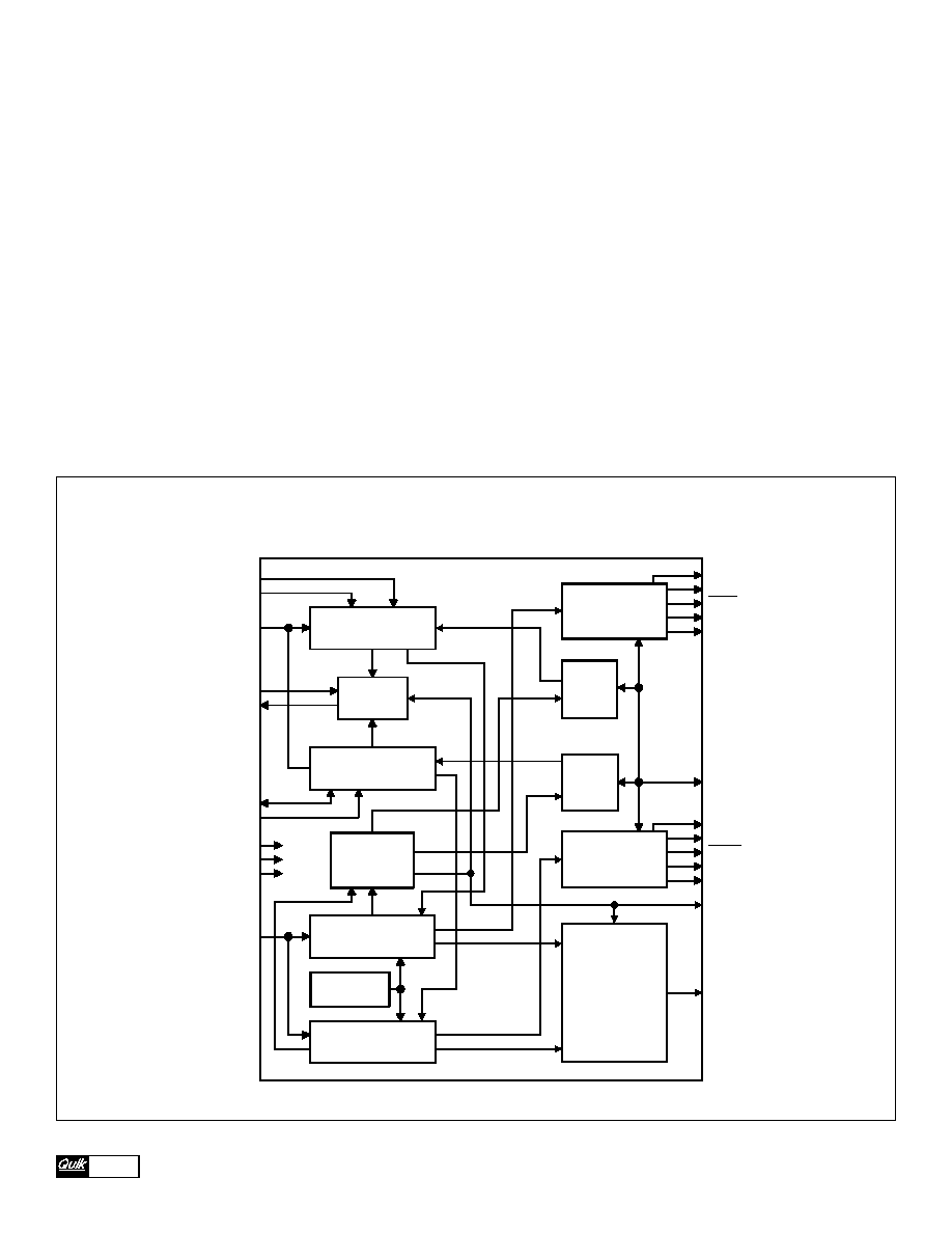
VOICE
CHA
SEGMENT CONTROL
BANK
CONTROL
CHB
SEGMENT CONTROL
CHA & CHB
TIME SHARING
CIRCUIT
CHA CLOCK &
ADDRESS GENERATOR
HIGH SPEED
SPINNER
CHB CLOCK &
ADDRESS GENERATOR
CHA CVSD
DEMODULATOR
CHA
FLAG
RECEIVER
CHB
FLAG
RECEIVER
CHB CVSD
DEMODULATOR
ADDRESS
MULTIPLEXER
ANGD1
ANG1
ANG1
ENV1
INT1
ANGD2
ANG2
ANG2
ENV2
INT2
D0 ~ D7
ECS
A0 ~ A19
OSC1 & OSC2
I/O2
RESET2
INE, INF
SE, SF
INA ~ IND
I/O1
RESET1
VCC
VDS
VAS
Block Diagram

VP-1608..........................................................................................5
VOICE
ENV2:
Envelop input for channel B, to be connected to INT2 with
a feedback resistor.
INT1:
Integrator output for channel A, to be connected to an
external RC integration circuitry.
INT2:
Integrator output for channel B, to be connected to an
external RC integration circuitry.
I/O1:
Strobe input/Busy output for channel A, active low. To
play a message on channel A, place the segment/bank
code on INA to INE and strobe this pin with a low pulse.
During the playback this pin becomes an active-low "busy"
output. If this pin is held low at the end of playback, the
message will be re-triggered.
I/O2:
Same as I/O1 except that this pin is for channel B.
INA ~ IND:
Input for segment code in binary format. INA is the LSB
and IND is the MSB.
INE, INF:
Input for bank code in binary format, max. 4 banks. INE is
the LSB and INF is the MSB.
OSC1, OSC2:
Internal oscillator pins for external RC components. It
external clock source is to be used, feed it through the
OSC2 pin. Note that both channels share the same clock,
so their sampling rate must be the same.
RESET1:
Reset input for channel A, active low. On the falling edge
of this reset signal, channel A playback is stopped and all
internal counters for channel A are cleared.
RESET2:
Reset input for channel B, active low. On the falling edge
of this reset signal, channel B playback is stopped and all
internal counters for channel B are cleared.
SCK, TEST:
For factory use only, do not make any connection.
SE, SF:
Output for EPROM bank select. These two pins are actually
latched outputs for INE and INF.
VDD:
Input, supply voltage.
VDS & VAS:
VDS is digital ground and VAS is analog ground. Connect
the two grounds together close to the power source to
minimize noise.
APPLICATION NOTES
1. EOM (End Of Message) Flag
The EOM flag consists of six consecutive bytes of "AA", or
"10101010" in binary format. After a trigger signal is
received, the VP-1608 uses the internal 8MHz system clock
to scan through memory space and finds the correct
message by counting the number of EOM flags. For
example, to find the 5th message, it must scan through
each and every memory location until it finds 4 EOM flags.
The first byte following the 4th EOM flag is the first byte
of the 5th message.
2. Creating Master EPROM File on the VP-880 System
Follow these steps to create the master EPROM file:
1. To maximize the EPROM usage, arrange your sound
segments in banks of 16 or less, so that the total combined
length for each bank is about the same. Do not mix
channel A and channel B together.
2. Based on the total combined length of the largest bank,
select a highest sampling rate that will fully utilize the
EPROM. Use the following equation:
Sampling Rate (Kbps) =
EPROM Size (K-bits) / Total Length (Second)
3. Digitize and edit each segment as a separate file. Use
the "ROM Data Management" function to combine up to
16 messages into a "bank file". The first filename entered
in the "ROM Data Management" is the first segment in that
bank, and etc.
4. Depending on the hardware design, each EPROM chip
may contain one or more sound banks. It is also possible
to use just one EPROM to store all sound segments of both
channel A and channel B. If you need to combine several
bank files into one for programming into one EPROM chip,
use the following DOS command:
COPY /b file_1+file_2+..+file_n destination_file
Do not use the "ROM Data Management" function to
combine bank files, otherwise each bank file will be
considered as a single message file.