COMSET SEMICONDUCTORS
1/3
The BD683 is NPN eptaxial-base transistors in monolithic Darlington circuit for audio
and video applications.
They are mounted in Jedec TO-126 plastic package.
PNP complement is BD684.
SILICON DARLINGTON POWER
TRANSISTORS
NPN BD683
PNP BD684
ABSOLUTE MAXIMUM RATINGS
Symbol
Ratings
Value
Unit
V
CEO
Collector-Emitter Voltage
120
V
V
CBO
Collector-Base Voltage
140
V
V
EBO
Emitter-Base Voltage
5
V
I
C
4
I
C
Collector Current
I
CM
6
A
I
B
Base current (peak value)
I
BM
0.1
A
P
T
Total power Dissipation
@ T
mb
= 25°C
40
Watts
T
J
Junction Temperature
150
°C
T
Stg
Storage Temperature
-65 to +150
°C
THERMAL CHARACTERISTICS
Symbol
Ratings
Value
Unit
R
thJ-mb
Thermal Resistance, Junction to mouting base
3.12
K/W
R
thJ-a
Thermal Resistance, Junction to ambient in free air
100
K/W
COMSET SEMICONDUCTORS
2/3
NPN BD683
PNP BD684
ELECTRICAL CHARACTERISTICS
TC=25°C unless otherwise noted
Symbol
Ratings
Test Condition(s)
Min Typ Max Unit
I
E
=0 ,
V
CB
= V
CEOMAX
=120 V
-
-
0,2
I
CBO
Collector cut-off current
I
E
=0 ,
V
CB
= 1/2V
CBOMAX
= 70V,T
j
= 150°C
-
-
1
mA
I
CEO
Collector cut-off current
I
B
=0 ,
V
CE
= 1/2V
CEOMAX
=60 V
-
-
0,2
mA
I
EBO
Emitter cut-offcurrent
I
C
=0, V
EB
=5 V
-
-
5
mA
V
CE(SAT)
Collector-Emitter saturation
Voltage
I
C
=1.5 A, I
B
=6 mA
-
-
2,5
V
V
CE
=3 V, I
C
=500 mA
-
2200
-
V
CE
=3 V, I
C
=1,5 A
750
-
-
h
FE
DC Current Gain
V
CE
=3 V, I
C
=4 A
-
1500
-
V
BE
Base-Emitter Voltage(1&2)
V
CE
=3 V, I
C
=1,5 A
-
-
2,5
V
h
fe
Small signal current gain
V
CE
=3 V, I
C
=1,5 A, f= 1 MHz
10
-
-
f
hfe
Ut-off frequency
V
CE
=3 V, I
C
=1,5 A
-
60
-
kHz
V
F
Diode forward voltage
I
F
=1,5 A
I
(SB)
Second-breakdown collector
current
V
CE
=50 V, t
P
= 20ms,non rep., without
heatsink
0,8
-
-
A
t
on
Turn-on time
-
0,8
2
t
off
Turn-off time
I
con
= 1,5A, I
bon
= -I
boff
= 6mA, V
CC
=30V
-
4,5
8
µs
1. Measured under pulse conditions :
t
P
<300µs,
<2%.
2.
V
BE
decreases by about 3,6 mV/K with increasing temperature.
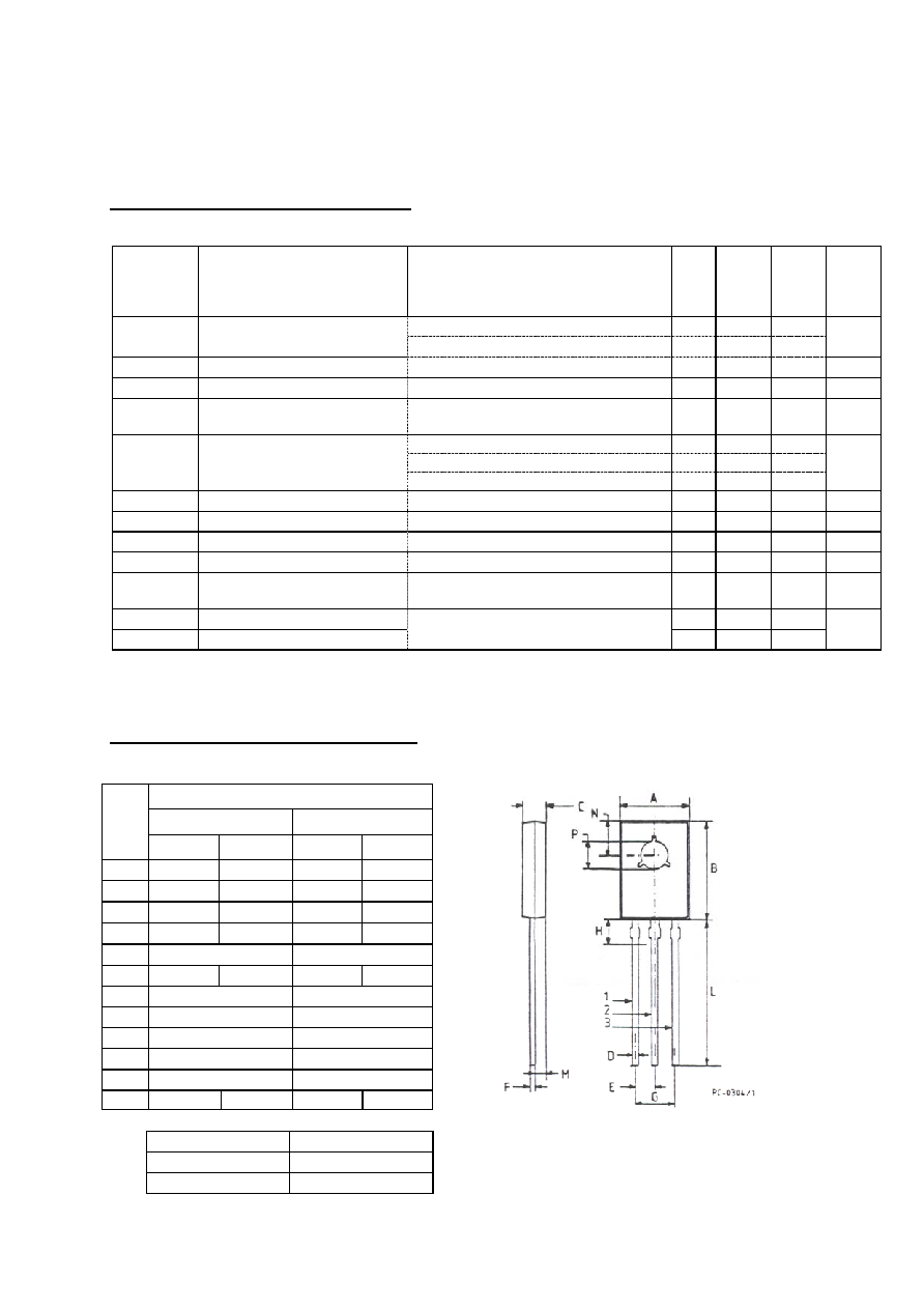
MECHANICAL DATA CASE TO-126
DIMENSIONS
mm
inches
min
max
min
max
A
7.4
7.8
0.295
0.307
B
10.5
10.8
0.413
0.425
C
2.4
2.7
0.094
0.106
D
0.7
0.9
0.027
0.035
E
2.2 typ.
0.087 typ.
F
0.49
0.75
0.019
0.029
G
4.4 typ.
0.173 typ.
H
2.54 typ.
0.100 typ.
L
15.7 typ.
0.618 typ.
M
1.2 typ.
0.047 typ.
N
3.8 typ.
0.149 typ.
P
3.0
3.2
0.118
0.126
Pin 1 :
Emitter
Pin 2 :
Collector
Pin 3 :
Base

COMSET SEMICONDUCTORS
3/3
Information furnished is believed to be accurate and reliable. However, CS assumes no responsability
for the consequences of use of such information nor for errors that could appear.
Data are subject to change without notice.