 | ÐлекÑÑоннÑй компоненÑ: AG203-63 | СкаÑаÑÑ:  PDF PDF  ZIP ZIP |
Äîêóìåíòàöèÿ è îïèñàíèÿ www.docs.chipfind.ru
Specifications and information are subject to change without notice
WJ Communications, Inc
·
Phone 1-800-WJ1-4401
·
FAX: 408-577-6621
·
e-mail: sales@wj.com
·
Web site: www.wj.com
April
2004
AG203-63
InGaP HBT Gain Block
Product Information
The Communications Edge
TM
Product Features
·
DC 6000 MHz
·
+8 dBm P1dB at 900 MHz
·
+20 dBm OIP3 at 900 MHz
·
20 dB Gain at 900 MHz
·
Single Voltage Supply
·
SOT-363 SMT Package
·
Internally matched to 50
Applications
·
Mobile Infrastructure
·
CATV / DBS
·
W-LAN / ISM
·
RFID
·
Defense / Homeland Security
·
Fixed Wireless
Product Description
The AG203-63 is a general-purpose buffer amplifier that
offers high dynamic range in a low-cost surface-mount
package. At 900 MHz, the AG203-63 typically provides
20 dB of gain, +20 dBm Output IP3, and +8 dBm P1dB.
The device combines dependable performance with
consistent quality to maintain MTTF values exceeding 100
years at mounting temperatures of +85
° C and is housed in
a SOT-363 industry-standard SMT package.
The AG203-63 consists of Darlington pair amplifiers using
the high reliability InGaP/GaAs HBT technology process
technology and only requires DC-blocking capacitors, a
bias resistor, and an inductive RF choke for operation.
The broadband MMIC amplifier can be directly applied to
various current and next generation wireless technologies
such as GPRS, GSM, CDMA, and W-CDMA. In addition,
the AG203-63 will work for other various applications
within the DC to 6 GHz frequency range such as CATV
and fixed wireless.
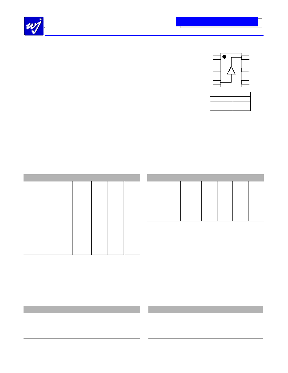
Functional Diagram
RF IN
GND
RF OUT
GND
GND
GND
1
2
3
4
6
5
Function Pin
No.
Input 3
Output/Bias 6
Ground
1, 2, 4, 5
Specifications
Parameter
Units Min Typ Max
Frequency Range
MHz
DC
900
6000
Gain (900 MHz)
dB
19.7
Gain (1900 MHz)
dB
16.8
17.8
18.8
Input
Return
Loss
dB 20
Output Return Loss
dB
16
Output P1dB
dBm
+8.0
Output IP3 (2)
dBm
+20.1
Output IP2
dBm
+24
Noise
Figure
dB 3.0
Device Voltage
V
4.05
Device Current
mA
20
Thermal Resistance
°C / W
472
Junction Temperature (3)
°C 177
Test conditions unless otherwise noted.
1. T = 25º C, Supply Voltage = +5 V, R
bias
= 47.5
, Frequency = 900 MHz, 50 System.
2. 3OIP measured with two tones at an output power of -10 dBm/tone separated by 10 MHz. The
suppression on the largest IM3 product is used to calculate the 3OIP using a 2:1 rule.
3. The junction temperature ensures a minimum MTTF rating of 1 million hours of usage.
Typical Performance
Parameter
Units
Typical
Frequency MHz
500
900
1900
2140
S21 dB
20.3
19.7
17.7
17.3
S11
dB -25 -20 -18 -16
S22
dB -16 -16 -16 -16
Output P1dB
dBm
+8.1
+8.0
+7.4
+6.8
Output IP3
dBm
+20.2 +20.1 +19.7 +19.5
Noise
Figure
dB 2.9 3.0 3.2 3.2
Test conditions: T = 25º C, Supply Voltage = +5 V, R
bias
= 47.5
, 50 System.
Absolute Maximum Rating
Ordering Information
Parameter
Rating
Part No.
Description
Operating Case Temperature
-40 to +85
°C
AG203-63
InGaP HBT Gain Block
Storage Temperature
-55 to +125
°C
AG203-63PCB 700 2400 MHz Fully Assembled Eval. Board
DC Voltage
+4.5 V
RF Input Power (continuous)
+10 dBm
Junction Temperature
+250
° C
Operation of this device above any of these parameters may cause permanent damage.
Specifications and information are subject to change without notice
WJ Communications, Inc
·
Phone 1-800-WJ1-4401
·
FAX: 408-577-6621
·
e-mail: sales@wj.com
·
Web site: www.wj.com
April
2004
AG203-63
InGaP HBT Gain Block
Product Information
The Communications Edge
TM
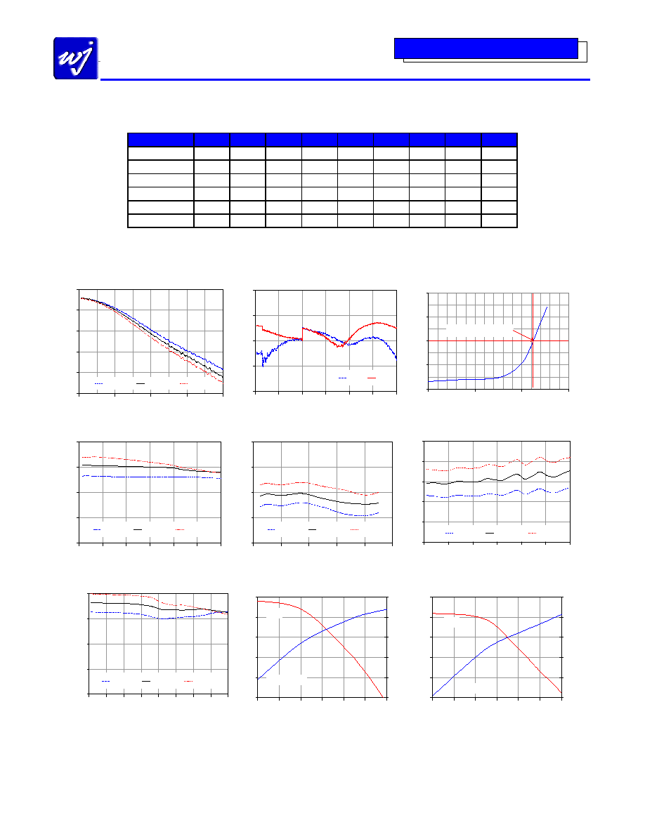
Typical Device RF Performance
Supply Bias = +5 V, R
bias
= 47.5
, I
cc
= 20 mA
Frequency
MHz
100
500
900
1900
2140
2400
3500
5800
S21 dB
20.4
20.3
19.7
17.7 17.3 16.7 14.9 11.5
S11
dB -25 -25 -20 -18 -16 -16 -20 -20
S22
dB -14 -16 -16 -16 -16 -16 -20 -14
Output P1dB
dBm
+8.2
+8.1
+8.0 +7.4 +6.8 +6.8 +6.6
Output IP3
dBm
+20.3
+20.2
+20.1 +19.7 +19.5 +19.5
Noise
Figure dB 2.9 2.9 3.0 3.2 3.2 3.3
1. Test conditions: T = 25º C, Supply Voltage = +5 V, Device Voltage = 4.05 V, Rbias = 47.5
, I = 20 mA typical, 50 System.
2. 3OIP measured with two tones at an output power of -10 dBm/tone separated by 10 MHz. The suppression on the largest IM3 product is used to calculate the 3OIP using a 2:1 rule.
3. Data is shown as device performance only. Actual implementation for the desired frequency band will be determined by external components shown in the application circuit.
Gain vs. Frequency
12
14
16
18
20
22
0
1
2
3
4
Frequency (GHz)
Gain
(
d
B
)
-40 C
+25 C
+85 C
Return Loss
-40
-30
-20
-10
0
0
1
2
3
4
5
6
Frequency (GHz)
S11,
S22
(
dB
)
S11
S22
I-V Curve
0
10
20
30
40
3.0
3.5
4.0
4.5
Device Voltage (V)
Devi
ce Cu
rren
t
(
mA
)
Optimal operating point
Output IP3 vs. Frequency
5
10
15
20
25
0
0.5
1
1.5
2
2.5
3
Frequency (GHz)
OIP3
(
dBm
)
-40 C
+25 C
+85 C
Output IP2 vs. Frequency
15
20
25
30
35
0
200
400
600
800
1000
Frequency (MHz)
OIP2
(
dBm
)
-40c
+25c
+85c
Noise Figure vs. Frequency
0
1
2
3
4
5
0
0.5
1
1.5
2
2.5
3
Frequency (GHz)
NF
(d
B)
-40 C
+25 C
+85 C
P1dB vs. Frequency
-10
-5
0
5
10
0
0.5
1
1.5
2
2.5
3
3.5
4
Frequency (GHz)
P1dB
(
dBm
)
-40 C
+25 C
+85 C
Output Power / Gain vs. Input Power
frequency = 900 MHz
10
12
14
16
18
20
-20
-16
-12
-8
-4
0
4
Input Power (dBm)
Gai
n
(d
B
)
-4
0
4
8
12
16
Ou
t
p
u
t
P
o
we
r
(
d
B
m
)
Output Power
Gain
Output Power / Gain vs. Input Power
frequency = 2000 MHz
8
10
12
14
16
18
-20
-16
-12
-8
-4
0
4
Input Power (dBm)
Gai
n
(d
B
)
-4
0
4
8
12
16
Ou
t
p
u
t
P
o
we
r
(
d
B
m
)
Output Power
Gain
Specifications and information are subject to change without notice
WJ Communications, Inc
·
Phone 1-800-WJ1-4401
·
FAX: 408-577-6621
·
e-mail: sales@wj.com
·
Web site: www.wj.com
April
2004
AG203-63
InGaP HBT Gain Block
Product Information
The Communications Edge
TM
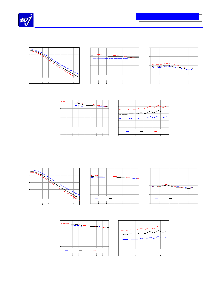
Typical Device RF Performance (cont'd)
Supply Bias = +6 V, R
bias
= 98
, I
cc
= 20 mA
Gain vs. Frequency
12
14
16
18
20
22
0
1
2
3
4
Frequency (GHz)
Gain
(
d
B
)
-40 C
+25 C
+85 C
Output IP3 vs. Frequency
5
10
15
20
25
0
0.5
1
1.5
2
2.5
3
Frequency (GHz)
OIP3
(
dBm
)
-40 C
+25 C
+85 C
Output IP2 vs. Frequency
15
20
25
30
35
0
200
400
600
800
1000
Frequency (MHz)
OIP2
(
dBm
)
-40c
+25c
+85c
P1dB vs. Frequency
-10
-5
0
5
10
0
0.5
1
1.5
2
2.5
3
3.5
4
Frequency (GHz)
P1dB
(
dBm
)
-40 C
+25 C
+85 C
Noise Figure vs. Frequency
0
1
2
3
4
5
0
0.5
1
1.5
2
2.5
3
Frequency (GHz)
NF
(d
B)
-40 C
+25 C
+85 C
Typical Device RF Performance
Supply Bias = +8 V, R
bias
= 198
, I
cc
= 20 mA
Gain vs. Frequency
12
14
16
18
20
22
0
1
2
3
4
Frequency (GHz)
Gain
(
d
B
)
-40 C
+25 C
+85 C
Output IP3 vs. Frequency
5
10
15
20
25
0
0.5
1
1.5
2
2.5
3
Frequency (GHz)
OIP3
(
dBm
)
-40 C
+25 C
+85 C
Output IP2 vs. Frequency
15
20
25
30
35
0
200
400
600
800
1000
Frequency (MHz)
OIP2
(
dBm
)
-40c
+25c
+85c
P1dB vs. Frequency
-10
-5
0
5
10
0
0.5
1
1.5
2
2.5
3
3.5
4
Frequency (GHz)
P1dB
(
dBm
)
-40 C
+25 C
+85 C
Noise Figure vs. Frequency
0
1
2
3
4
5
0
0.5
1
1.5
2
2.5
3
Frequency (GHz)
NF
(d
B)
-40 C
+25 C
+85 C
Specifications and information are subject to change without notice
WJ Communications, Inc
·
Phone 1-800-WJ1-4401
·
FAX: 408-577-6621
·
e-mail: sales@wj.com
·
Web site: www.wj.com
April
2004
AG203-63
InGaP HBT Gain Block
Product Information
The Communications Edge
TM
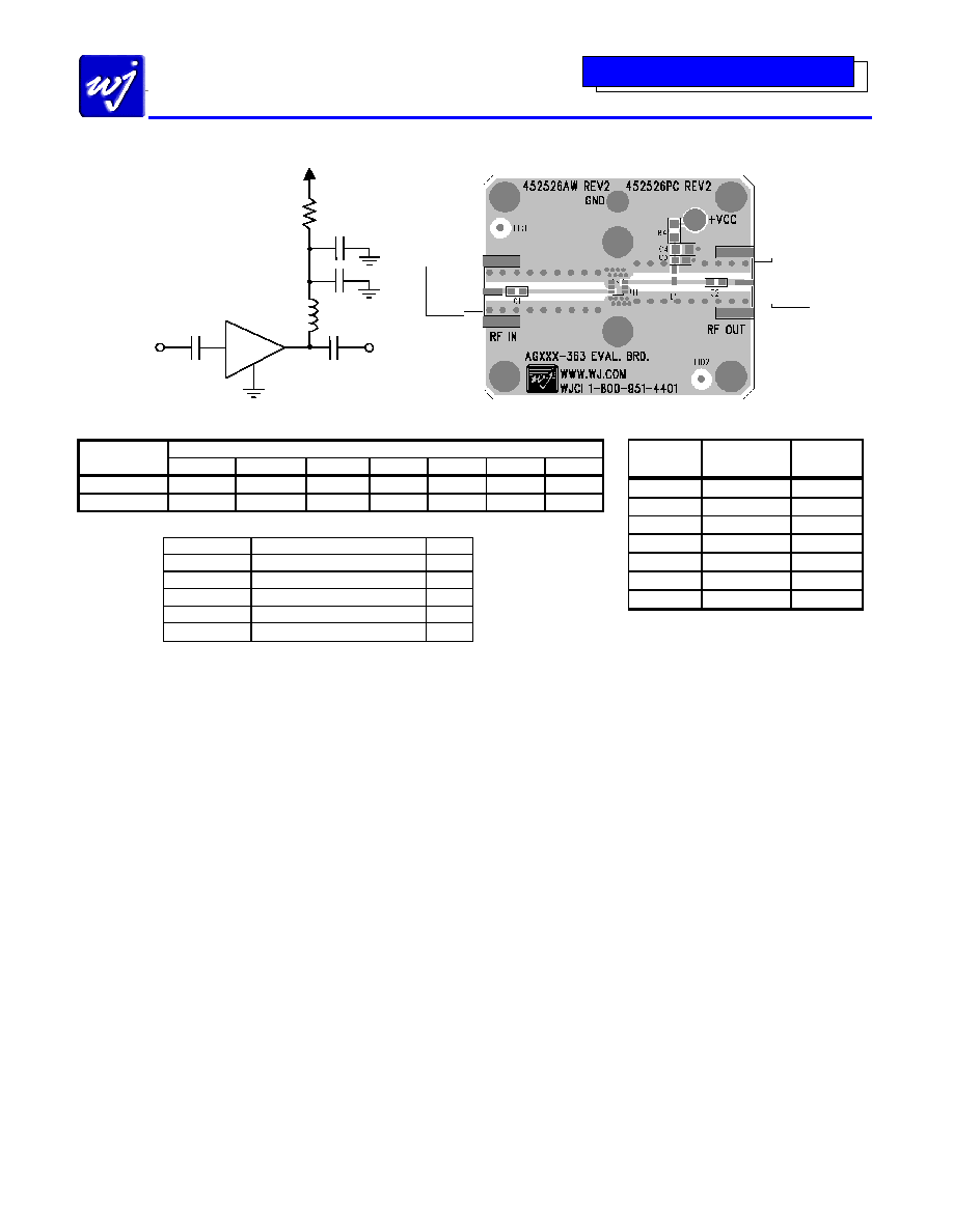
Application Circuit
Recommended Component Values
Reference
Frequency (MHz)
Designator
50
500 900 1900 2200 2500 3500
L1
820 nH
220 nH
68 nH
27 nH
22 nH
18 nH
15 nH
C1, C2, C4
.018 µF
1000 pF
100 pF
68 pF
68 pF
56 pF
39 pF
1. The proper values for the components are dependent upon the intended frequency of operation.
2. The following values are contained on the evaluation board to achieve optimal broadband performance:
Ref. Desig.
Value / Type
Size
L1
39 nH wirewound inductor
0603
C1, C2
56 pF chip capacitor
0603
C3
0.018
µF chip capacitor
0603
C4
Do Not Place
R1
47.5
1% tolerance
0603
Recommended Bias Resistor Values
S upply
Voltage
R1 value
Size
5 V
47.5 ohms
0603
6 V
98 ohms
0603
7 V
148 ohms
0805
8 V
198 ohms
0805
9 V
248 ohms
1206
10 V
298 ohms
1210
12 V
398 ohms
1210
The proper value for R1 is dependent upon the supply
voltage and allows for bias stability over temperature.
WJ recommends a minimum supply bias of +5 V. A
1% tolerance resistor is recommended.
C1
Blocking
Capacitor
RF OUT
L1
RF Choke
C3
0.018 µF
R1
Bias
Resistor
RF IN
C4
Bypass
Capacitor
C2
Blocking
Capacitor
Vcc
Icc = 20 mA
AG203-63
Specifications and information are subject to change without notice
WJ Communications, Inc
·
Phone 1-800-WJ1-4401
·
FAX: 408-577-6621
·
e-mail: sales@wj.com
·
Web site: www.wj.com
April
2004
AG203-63
InGaP HBT Gain Block
Product Information
The Communications Edge
TM
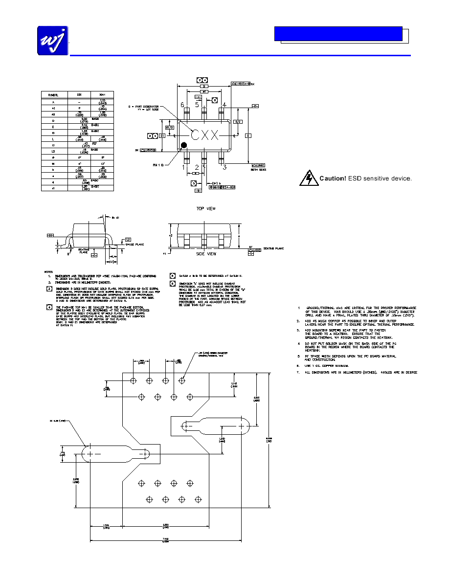
Outline Drawing
Land Pattern
Product Marking
The component will be marked with a "C"
designator followed by a two-digit numeric
lot code on the top surface of the package.
Tape and reel specifications for this part are
located on the website in the "Application
Notes" section.
MSL / ESD Rating
ESD Rating: Class 1C
Value:
Passes at 1000 V min.
Test:
Human Body Model (HBM)
Standard:
JEDEC Standard JESD22-A114
ESD Rating: Level 4
Value:
Passes at 1000 V min.
Test:
Charged Device Model (CDM)
Standard:
JEDEC Standard JESD22-C101
MSL Rating: Level 1
Standard:
JEDEC Standard J-STD-020A
Mounting Config. Notes