 | ÐлекÑÑоннÑй компоненÑ: AG101 | СкаÑаÑÑ:  PDF PDF  ZIP ZIP |
Äîêóìåíòàöèÿ è îïèñàíèÿ www.docs.chipfind.ru
WJ Communications, Inc. · Phone: 1-800-WJ1-4401 · FAX: 408-577-6620 · e-mail: sales@wj.com · Web site: www.wj.com
April 2002
AG101
Product Description
The AG101 is a general purpose gain block that
offers good dynamic range in a low cost surface
mount package. The combination of flat OIP3
and noise figure performance over frequency
makes it attractive for for both narrow band
and broadband applications. Superior thermal
design allows the product to achieve +32 dBm
OIP3 performance at a mounting temperature
of +85°C with an associated MTBF of >1000
years
3
. All devices are 100% RF and DC tested.
Product Features
·
60 - 3000 MHz
·
+
32 dBm Output IP3
·
2.4 dB Noise Figure
·
14 dB Gain
·
+
15 dBm P1dB
·
MTBF >1000 Years
·
SOT-89 SMT Package
·
Single Bias Supply
(+3.3 V or +4.5 V)
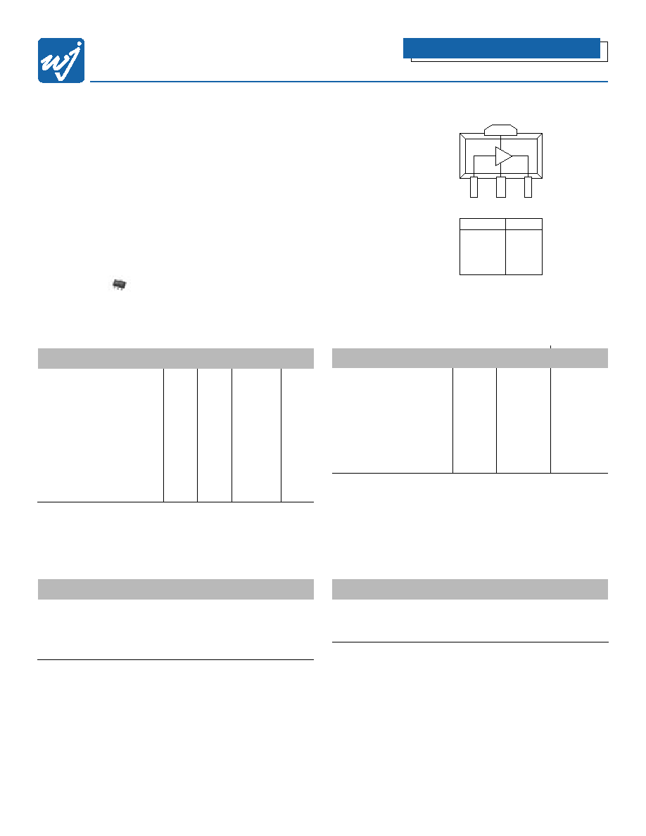
Functional Diagram
4
1
2
3
Function Pin
No.
Input
1
Ground
2
Output/Bias
3
Ground
4
High Dynamic Range Gain Block
Recommended Maximum Ratings
Parameter
Rating
Operating Case Temperature
-40 to +85°C
Storage Temperature
-55 to +125°C
DC Voltage +5.5 V
RF Input Power (continuous)
+4 dBm
Operation of this device above any of these parameters may cause permanent damage.
Ordering Information
Part No.
Description
AG101
GaAs MMIC Amplifier
(Available in tape and reel)
AG101-PCB
Fully Assembled Application Circuit
The Communications Edge
TM
Advanced Product Information
Specifications
Parameter
Units
Min.
Typical
Max.
Frequency Range MHz 60-3000
S21 - Gain dB 13.0 14.0 16.0
S11 - Input Return Loss
dB
-9.0
S22 - Output Return Loss
dB
-15.0
Output IP3 dBm +28 +32 +36
Output P1dB
dBm
+15
Noise Figure
dB
2.4
Operating Current Range
mA
40
50
75
Supply Voltage
V
4.5
Test conditions unless otherwise noted.
1. T = 25°C, Vdd = 4.5 V, Frequency = 800 MHz, 50 ohm system.
2. 3OIP measured with two tones at an output power of 2 dBm/tone separated by 10 MHz. The
suppression on the largest IM3 product is used to calculate the 3OIP using a 2:1 slope rule.
3. MTBF calculated with ground lead temperature at 85°C.
4. S11 can be improved using an optional matching network.
Typical Parameters
Parameter
Units
Typical
Frequency MHz
900
1900
S21 dB
13.4
12.2
S11
dB
-12.5
-13.2
S22
dB
-21.2
-17.8
Output IP3
dBm
+32.5
+33.1
Output P1dB
dBm
+15.1
+15.0
Noise Figure
dB
2.4
2.6
Typical parameters reflect performance in an applicaton circuit.
Actual Size
WJ Communications, Inc. · Phone: 1-800-WJ1-4401 · FAX: 408-577-6620 · e-mail: sales@wj.com · Web site: www.wj.com
April 2002
AG101
Advanced Product Information
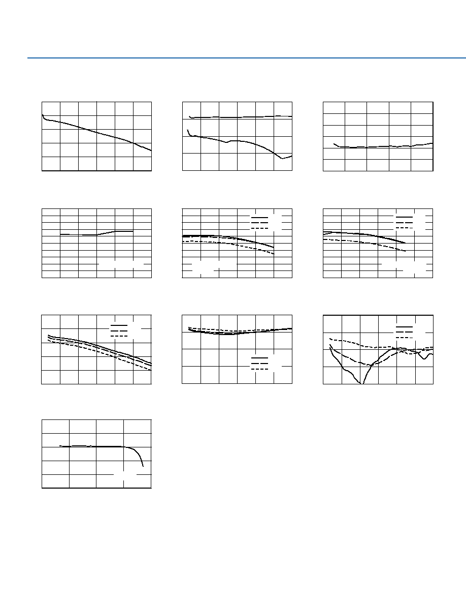
Performance Charts
(Vd = 4.5 V, Id = 50 mA, T = 25°C)
0
16
14
12
10
18
S21 (dB)
8
2000
2500
3000
Frequency (MHz)
500
1000
1500
0
2000
2500
3000
500
1000
1500
Gain vs. Frequency
-10
-20
-30
S11
S22
-40
Return Loss (db)
0
Return Loss vs. Frequency
0
2000
2500
3000
Frequency (MHz)
500
1000
1500
0
1800
2400
3000
Frequency (MHz)
600
1200
32
30
28
26
24
22
20
IP3 (dBm)
36
34
38
40
OIP3 vs. Pout
0
2
4
6
8
10
12
Pout (dBm)
1900 MHz
34
28
26
38
40
36
32
30
22
24
IP3 (dBm)
20
OIP3 vs. Pout
800 MHz
32
28
40
36
24
30
26
38
34
22
OIP3 (dBm)
20
OIP3 vs. Frequency
Frequency (MHz)
4
3
6
5
2
1
NF (dB)
0
NF vs. Frequency
18
16
14
12
10
Gain (dB)
8
Gain vs. Pout
0
20
Pout (dBm)
5
10
15
800MHz
18
14
12
10
16
8
S21 (dB)
S21 vs. Frequency over Temperature
0
2000
2500
3000
Frequency (MHz)
500
1000
1500
-10
0
-20
-30
-40
S11 (dB)
S11 vs. Frequency over Temperature
0
2000
2500
3000
Frequency (MHz)
500
1000
1500
-10
-20
-30
-40
S22 (dB)
S22 vs. Frequency over Temperature
0
0
2000
2500
3000
Frequency (MHz)
500
1000
1500
-40
°
C
25
°
C
80
°
C
-40
°
C
0
°
C
80
°
C
-40
°
C
0
°
C
80
°
C
-40
°
C
25
°
C
80
°
C
-40
°
C
25
°
C
80
°
C
Pout = 2 dBm/tone
Pout = 2 dBm/tone
Pout = 2 dBm/tone
8
10
12
Pout (dBm)
0
2
4
6
WJ Communications, Inc. · Phone: 1-800-WJ1-4401 · FAX: 408-577-6620 · e-mail: sales@wj.com · Web site: www.wj.com
April 2002
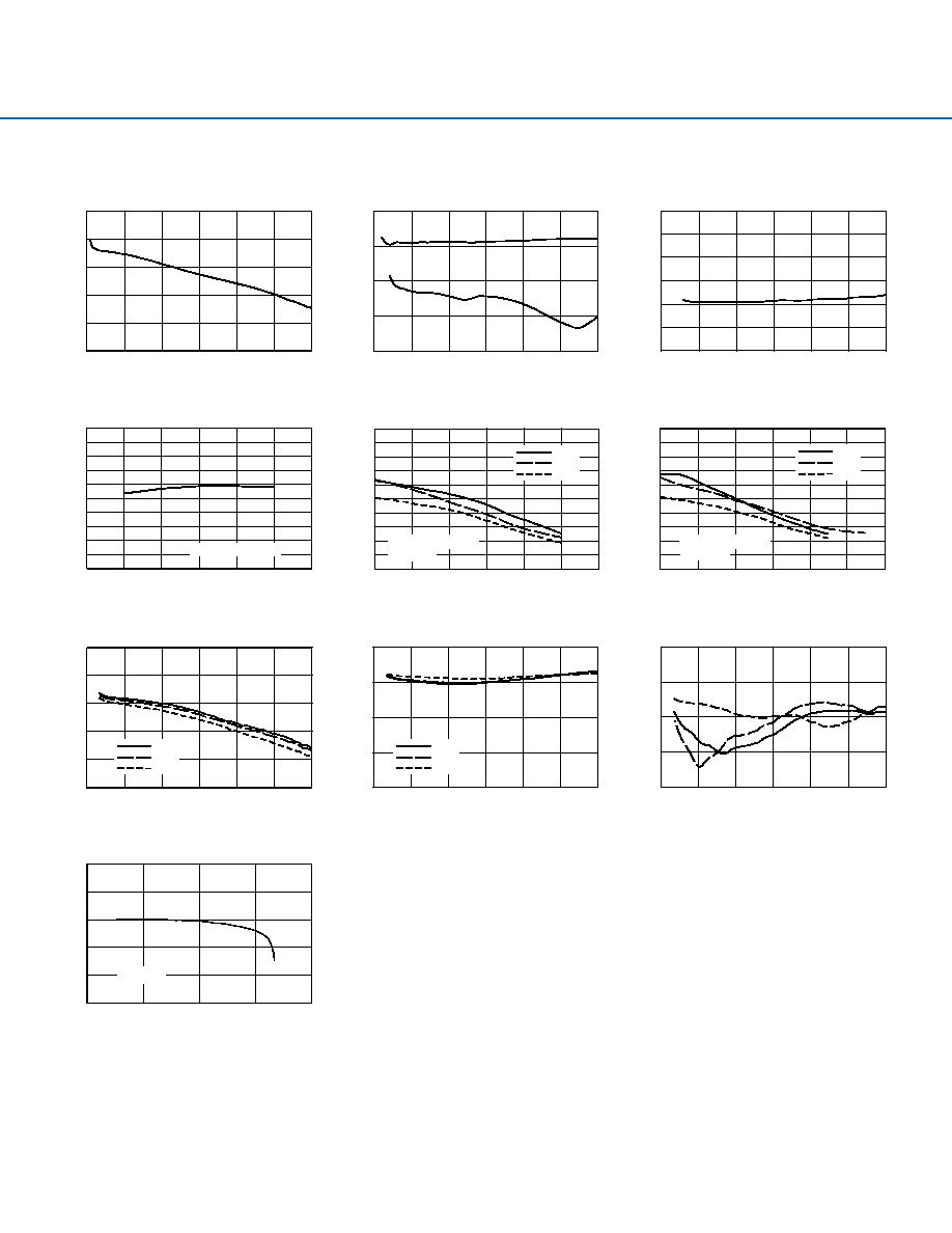
Performance Charts
(Vd = 3.3 V, Id = 50 mA, T = 25°C)
18
16
12
14
10
S21 (dB)
0
8
2000
2500
3000
Frequency (MHz)
500
1000
1500
Gain vs. Frequency
Return Loss vs. Frequency
0
-10
-20
-30
S11
S22
-40
Return Loss (dB)
2000
2500
3000
Frequency (MHz)
0
500
1000
1500
OIP3 vs. Frequency
30
32
28
24
26
40
36
38
34
22
OIP3 (dBm)
20
3000
Frequency (MHz)
0
500
1000
1500
2500
2000
Pout = 2 dBm/tone
8
10
12
Pout (dBm)
0
2
4
6
40
36
34
30
38
32
28
26
24
22
20
OIP3 (dBm)
OIP3 vs. Pout over Temperature
8
10
12
Pout (dBm)
0
2
4
6
38
32
30
40
34
36
28
26
24
22
20
OIP3 (dBm)
OIP3 vs. Pout over Temperature
800 MHz
-40
°
C
25
°
C
80
°
C
-40
°
C
25
°
C
80
°
C
6
5
4
3
2
500
0
1000
Frequency (MHz)
NF (dB)
1
0
2000
2500
3000
1500
NF vs. Frequency
-10
-20
-30
80
°
C
-40
-40
°
C
1500
2000
Frequency (MHz)
S22 (dB)
0
0
°
C
0
500
1000
2500
3000
S22 vs. Frequency over Temperature
18
16
14
12
10
8
S21 (dB)
1500
2000
Frequency (MHz)
0
500
1000
2500
3000
S21 vs. Frequency over Temperature
-40
-30
-20
-10
S11 (dB)
1500
2000
Frequency (MHz)
0
0
500
1000
2500
3000
S11 vs. Frequency over Temperature
18
14
12
10
16
Gain (dB)
8
Gain vs. Pout
800 MHz
1900 MHz
-40
°
C
0
°
C
80
°
C
-40
°
C
0
°
C
80
°
C
Pout = 2 dBm/tone
Pout = 2 dBm/tone
0
20
Pout (dBm)
5
10
15
WJ Communications, Inc. · Phone: 1-800-WJ1-4401 · FAX: 408-577-6620 · e-mail: sales@wj.com · Web site: www.wj.com
April 2002
AG101
Advanced Product Information
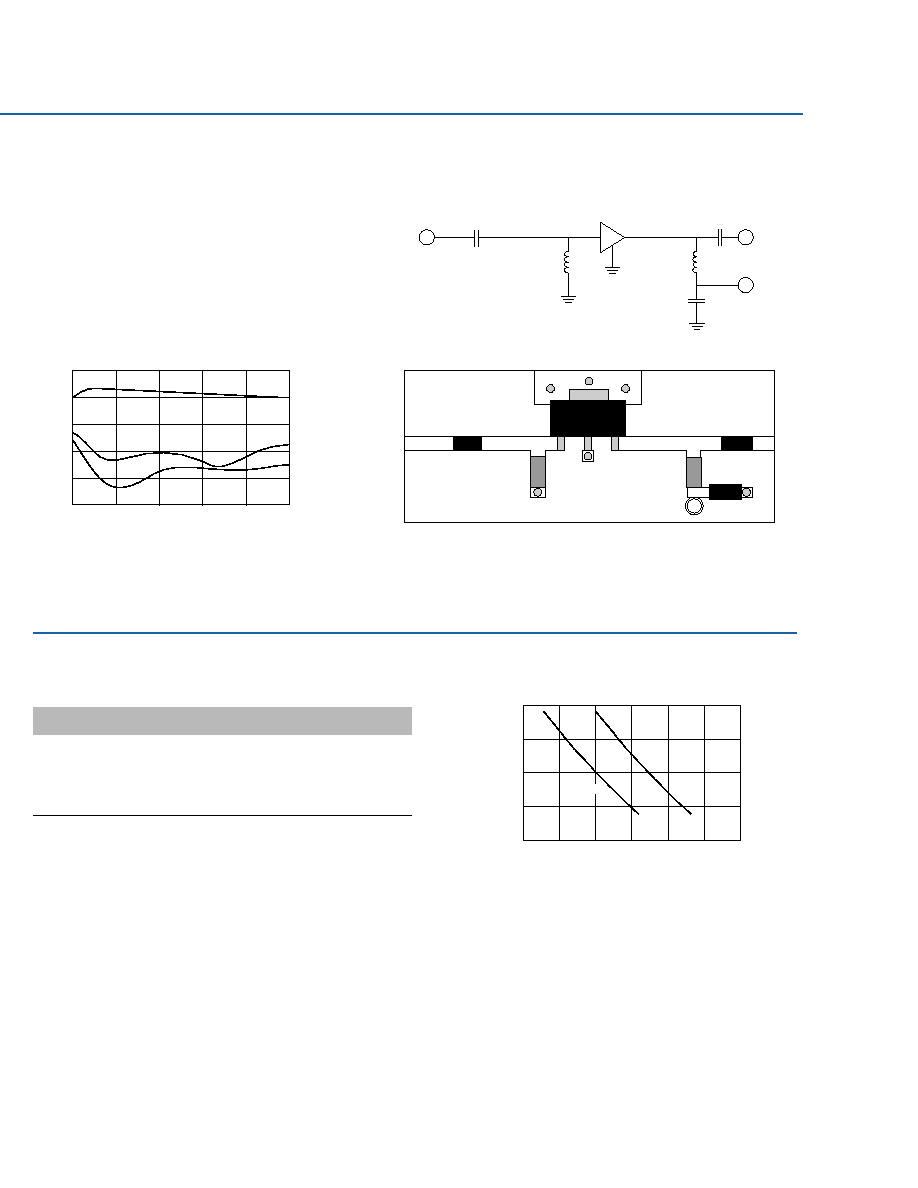
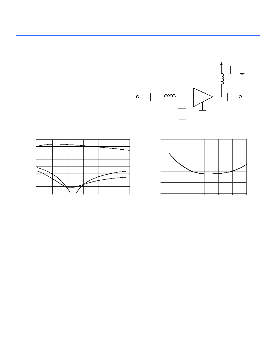
Application Circuit: 0.8 to 2.6 GHz
Frequency (MHz)
Magnitude (dB)
500
1000
1500
2000
3000
2500
S-Parameters
20
10
0
-10
-20
-30
Typical Specifications
Frequency
0.9 GHz
1.9 GHz
2.4 GHz
Magnitude S21
13.4 dB
12.2 dB
11.5 dB
Magnitude S11
-12.5 dB
-13.2 dB
-11.4 dB
Magnitude S22
-21.2 dB
-17.8 dB
-17.3 dB
OIP3
32.5 dBm 33.1 dBm 33.1 dBm
Noise Figure
2.4 dB
2.6 dB
2.8 dBm
Bias
Vds = 4.5 V, Id = 50 mA
FR4 Board Layout (T = 14 Mils)
Schematic
S21
S11
S22
AG101
C = 56 pF
RF OUT
RF IN
DC 4.5 V
C = 56 pF
L = 12 nH
L = 10 nH
GND
0603 Package
C = 56 pF
0603 Package
C = 56 pF
0603 Package
L = 12 nH
0603 Package
C = 56 pF
0603 Package
L = 10 nH
+4.5 V
INPUT
OUTPUT
C = 56 pF
3 or more Via
Grounds req.
All Trans. Lines Z = 50 Ohm
GND
NOTE: The application circuit is designed for wide bandwidth. For narrow band applications, S11 and S21 can be improved with an input shunt microstrip element to ground.
Thermal Specifications
Parameter
Rating
Operating Case Temperature
-40 to +85°C
Thermal Resistance (Maximum)
88°C/W
Junction Temperature
+155°C
(Recommended Maximum)
Notes:
1. Thermal Resistance determined at Maximum Tab Temperature and Maximum Power Dissipation.
2. Recommended Maximum Junction Temperature insures a MTBF of 1 million hours.
3. Refer to WJ Application Note "AG101 Temperature Effects on Reliability" for more information.
MTBF vs. Temperature
10
9
10
8
10
7
10
6
10
5
50
75
100
125
150
175
200
Junction
Ground Tab
MTBF (Hrs)
Temperature (
°
C)
WJ Communications, Inc
· Phone 1-800-WJ1-4401 · FAX: 408-577-6620 · e-mail: sales@wj.com · Web site: www.wj.com
April 2002
AG101
Application Circuit: 60 - 100 MHz
Typical Specifications
Frequency 70
MHz
Magnitude S21
16.3 dB
Magnitude S11
-17.1 dB
Magnitude S22
-15.6 dB
Noise Figure
5.1 dB
Bias Supply 4.5 V @
50 mA
Noise Figure
3
4
5
6
7
8
30
50
70
90
110
130
150
Frequency (MHz)
Noise Figure (dB)
S-Parameters
-20
-15
-10
-5
0
5
10
15
20
30
50
70
90
110
130
150
Frequency (MHz)
Magnitude (dB)
S21
S11
S22
RF IN
AG101
PIN 1
PIN 3
PIN 2,4
L1
180 nH
C1
.018
µF
RF OUT
L2
180 nH
V
DD
= + 4.5 V
I
D
= 75 mA
C3
.018
µF
C4
.018
µF
Schematic
C2
5.6 pF