
2051nt
ACC Microelectronics Corporation, 2500 Augustine Drive, Santa Clara, CA 95054
Phone: (408) 980-0622 Fax: (408) 980-0626
ACC MICRO 2051nt
PENTIUM-CLASS PCI SINGLE CHIP SOLUTION
FOR NOTEBOOK APPLICATIONS
DATA BOOK
ADVANCED INFORMATION
JANUARY 1997
Revision 3.0

ACC Micro
2051nt
TM
ACC Microelectronics Corporation, 2500 Augustine Drive, Santa Clara, CA 95054
Phone: (408) 980-0622 Fax: (408) 980-0626
ACC Microelectronics Corporation
2500 Augustine Drive,
Santa Clara, CA 95054
Phone: (408) 980-0622 Fax: (408) 980-0626
Copyright 1996 ACC Microelectronics Corporation. All rights reserved.
P/N 520210
Rev. 3.0
January 1997
Copyright
No part of this publication may be reproduced, transmitted, transcribed, stored in a retrieval system, or
translated into any language or computer language, in any form or by any means, electronic, mechanical,
magnetic, optical, chemical, manual, or otherwise, without the prior written permission of ACC
Microelectronics Corp, 2500 Augustine Drive, Santa Clara, CA 95054.
Disclaimer
ACC Microelectronics Corp. makes no representations or warranties with respect to the design and
documentation herein described and especially disclaims any implied warranties of merchantability or fitness
for any particular purpose. Further, ACC Microelectronics Corp. reserves the right to revise the design and
associated documentation and to make changes from time to time in the content without obligation of ACC
Microelectronics Corp. to notify any person of such revisions or changes.
Trademarks
Single Chip Solution is registered trademark of ACC Microelectronics Corp.
All other trademarks and copyrights are the property of their respective holders.

ACC Micro
2051nt
TM
i
Table of Contents
Title
Page
1.0
Introduction
1
1.1 ACC Micro 2051nt PCI Single Chip Solution Description
1
1.2 ACC Micro 2051nt PCI Single Chip Solution Features
1
1.3 ACC Micro 2051nt Block Diagram
3
2.0
Functional Description
4
2.1 L2 Cache
4
2.2 DRAM Interface
4
2.3 PCI Bus
4
2.4 Posted Write/Pre-fetch Buffers
4
2.5 Clock
4
2.6 Power Management Modes
5
2.6.1 Fully-On
5
2.6.2 Standby
5
2.6.3 Suspend
5
2.6.4 Doze
5
2.7 Idle Timers
6
2.7.1 Global-StandBy Timer
6
2.7.2 Auto-Suspend
6
2.7.3 Local-Standby Timers
6
2.7.4 Doze Timers
6
2.7.5 Warning Timers
6
2.8 SMM/SMIs
6
2.9 Thermal Control
7
2.10 Battery Management
7
2.11 AC Power
7
2.12 Mobile PC/PCI
7
2.13 CLKRUN#
7
2.14 Device I/O Shadowing
7
3.0
ACC Micro Pin Specifications
8
3.1 Pin Description
8
Table 3-1 Clock Interface
8
Table 3-2 CPU Interface
8
Table 3-3 Cache Interface
9
Table 3-4 DRAM Interface
11
Table 3-5 PCI Interface
11
Table 3-6 Reset Interface
12
Table 3-7 ISA Interface
12
Table 3-8 ISA/IRQ Interface
13
Table 3-9 ISA/XD Interface
14
Table 3-10 Real time Clock Interface
14
Table 3-11 Address Buffers Decodes Interface
14

ACC Micro
2051nt
TM
ii
Title
Page
Table 3-12 PC/PCI Interface
14
Table 3-13 PMC Interface
15
Table 3-14 Misc. Interface
15
3.2 ACC Micro 2051nt Numerical Pin Arrangement (w/ L2 Cache)
16
3.3 ACC Micro 2051nt Alphabetical Pin Arrangement (w/ L2 Cache)
18
3.4 ACC Micro 2051nt Summary Table for Multiplex Pins
20
3.5 ACC Micro 2051nt Power Plane Summany Table
23
3.6 ACC Micro 2051nt Shadow Register Application
24
4.0
ACC Micro 2051nt Register Settings
26
4.1 Device 0, Function 0 Configuration
27
4.1.1 PCI Range & Control
28
4.1.2 IDE Address
34
4.2 Memory Configuration
36
4.2.1 DRAM Configuration
37
4.2.2 L2 Cache Configuration
43
4.3 Power Management
48
4.3.1 Suspend Control
48
4.3.2 GPIO
50
4.4 Device 1, Function 0 Configuration
51
4.4.1 ISA Configuration
54
4.4.2 Chip Select Functions
57
4.4.3 ISA Peripheral Selection
60
4.5 Device 1, Function 1 Configuration
63
4.5.1 PCI IDE Control
64
4.6 Standard AT Configuration
70
4.6.1 SMI Registers
70
4.6.2 VRAM & Power Control
72
4.6.3 Doze Mode Control
74
4.6.4 Warning Timers
77
4.6.5 General Chip Select
79
4.6.6 Standby Control
84
4.6.7 Suspend Control
90
4.6.8 Battery Low Control
93
4.6.9 Thermal Control Through Software Emulation
96
4.6.10 STOP Clock Control
97
4.7 Interrupt Controller Register
99
4.7.1 IRQ7-IRQ3 Edge/Level Control Register
99
4.7.2 IRQ15-IRQ9 Edge/Level Control Register
100
5.0
ACC Micro 2051nt DC Specifications
101

ACC Micro
2051nt
TM
iii
Title
Page
6.0
ACC Micro 2051nt AC Specifications
104
6.1 Timing Diagrams
104
6.1.1 Propagation Delay
104
6.1.2 Valid Delay from Rising Clock Edge
104
6.1.3 Setup and Hold Times
104
6.1.4 Float Delay
104
6.1.5 Clock High and Low Timers and Period
105
6.1.6 Pulse Width
105
6.1.7 Output to Output Delay
105
6.2 Signals Timing
106
6.2.1 CLOCK Timing
106
6.2.2.CPU Interface Timing
106
6.2.3 Asynchronous Cache Interface Timing
107
6.2.4 Synchronous Cache Interface Timing
107
6.2.5 Fast Page Mode / EDO DRAM Interface Timing
108
6.2.6 PCI Interface Timing
108
6.2.7 AT Interface Timing
109
6.3 Functional Timing Diagram
110
6.3.1 Reset Timing
110
6.3.2 Shutdown Timing
110
6.3.3 AT Bus 16-Bit Access Timing
111
6.3.4 AT Bus 8-Bit Access Timing
112
6.3.5 Fast Page Mode DRAM Access Timing-Read Cycle
112
6.3.6 Fast Page Mode Access Timing-Write Cycle
113
6.3.7 EDO Page-Write Missed Cycle Timing
114
6.3.8 EDO Page-Read Missed Cycle Timing
115
6.3.9 Asynchronous SRAM Burst Read Cycle (3-2-2-2)
117
6.3.10 Asynchronous SRAM Burst Write Cycle (4-2-2-2)
117
6.3.11 Pipeline Synchronous SRAM Burst Read Cycle
118
6.3.12 Pipeline Synchronous SRAM Burst Write Cycle (3-1-1-1)
119
6.3.13 CPU-to-PCI Single Read
120
6.3.14 CPU-to-PCI Single Write, Write Buffer
121
6.3.15 CPU-to-PCI Multiple Write, Write-to-Buffer, PCI Burst Write122
7.0
ACC Micro 2051nt Pin Diagram
123
7.1.1 ACC Micro 2051nt
7.1.2 ACC Micro 2051nt Pin
7.1.3 ACC Micro 2051nt Mechanical Data Top View and Side View
125
7.1.4 ACC Micro 2051nt Mechanical Data - Top View
126
7.1.5 Package Dimensions
127
Appendix A-1 List of Sales Representatives

ACC Micro
2051nt
TM
1
ACC Micro 2051nt
PCI Single Chip Solution for Notebook Applications
Section 1 Introduction
1.1 Description
The ACC Micro 2051nt, PCI Single Chip Solution , is a true 64-bit high performance notebook solution to
support Intel Pentium, Cyrix M1, and AMD K5 microprocessors. The rich feature set of the ACC Micro
2051nt includes: level 2 write-back cache controller, DRAM controller, PCI interface, ISA interface, and ACC
Micro Power Management control. The integrated level 2 cache controller supports different types of SRAM
such as burst, pipeline burst, or standard asynchronous SRAM. Extended Data Output (EDO, and Fast Page
Mode DRAM are supported by the integrated DRAM controller. The built-in PCI bus interface can run in
synchronous or asynchronous mode with mobile/PCI support for docking designs.
ACC Micro Power Management allows the system power consumption to be controlled in various operation
modes such as Power-on suspend, Power-down suspend, Standby, and Doze. The whole system is partitioned
into four different power planes: CPU interface and level 2 cache interface, DRAM interface, PCI bus interface,
and ISA bus interface. Every power plane, except ISA (which is always at 5.0V) can be independently
configured to either 3.3V or 5.0V. No external level shifter is required.
1.2 Features
Supports Intel P54C, Cyrix M1, and AMD K5
Linear burst support
64-bit Pentium class CPU with 66 MHz bus frequency
ACC Micro Power Management Control
SMM/SMI support
Individual sets of system events and break events such as for Global Standby, Local Standby,
Suspend, and Doze control.
Dedicated external SMI trigger inputs such as for battery monitoring, suspend/resume button, and
AC power.
Software SMI
Warning Timer for SMI
Patented 'Adaptive Thermal Control' with auto-control or SMI generation
Shadow Registers for suspend to disk
Suspend to DRAM
CPU/PCI/ISA individually suspend/powered-down
Stop clock protocol, STPCLK#
0 Hz suspend
PCI suspend for Warm Docking
Mobile PC, or PC/PCI
CLKRUN# protocol to reduce PCI power consumption
Serialized interrupt protocol, SIN#/SOUT# for interrupt routing in docking design
Serialized DMA protocol for DRQ routing in docking design

ACC Micro
2051nt
TM
2
2051nt Features (continued)
Synchronous/asynchronous PCI bus
Synchronous PCI clock at CPUCLK/2
Asynchronous PCI clock
Four PCI bus masters
Converts back to back sequential CPU to PCI memory writes to PCI burst writes
Bytes merge for CPU to PCI memory write
Eight Dwords deep of CPU to PCI posted write buffers
Four Dwords pre-fetch buffers for CPU read from PCI memory
PCI to DRAM posting 8 Qwords deep
PCI from DRAM pre-fetched buffers 4 Qwords deep
Pre-snoop capability for PCI to DRAM with bandwidth of 119 MB/s
3V or 5V PCI bus
Built-in DRAM controller
Five banks of DRAM, up to 512MB main memory
Self-Refresh DRAM support
EDO or Fast Page Mode DRAM
Five RAS and 12 MA lines
Symmetrical/Asymmetrical DRAMs
64-bit data path to memory
64-bit DRAM option for individual bank
Four Qword posted write buffers for x-1-1-1 DRAM write cycles
Support 3V or 5V DRAM
Built-in level 2 cache controller
Direct mapped write back/write through
Up to 2MB
Burst, pipelined burst, or standard SRAM
Cache hit read/write x-1-1-1-1-1 ... with pipelined burst SRAM
Built-in full-blown ISA bus interface
Integrated 8254x1, 8259x2, 8237x2
Programmable ISA bus speed
Independent edge/level triggered interrupt controller
Optional Type-F DMA
X-bus support for chip select decode
Flash EPROM support
Dedicated ISA cycles option to free up the PCI bus
Integrated Fast IDE interface
Enhanced PCI IDE
Support master/DMA mode IDE
Built-in 8 Dwords posted write buffer
Built-in 8 Dwords pre-fetched buffer
Four independently programmable register sets for IDE timing control
Built-in 64-bit data path

ACC Micro
2051nt
TM
3
1.3
Block Diagram
TAG
CACHE
DRAM
CPU
2051nt
Ax
Dx
CPU Status
Keyboard Data, PS/2 Mouse
Enhanced IDE
EPROM
RTC
Super I/O
Audio
32-bit PCI Bus
MA, CAS
RAS
Power Management Control
ISA Bus

ACC Micro
2051nt
TM
4
Section 2 Functional Description
2.1 L2 Cache
A direct map level 2 cache controller is incorporated to support up to 2MBytes of SRAM by using either
burst, pipelined burst, or standard SRAM. A dynamic write-back/write-through algorithm is implemented
to optimize the bandwidth between cache and main memory. Alternatively, a cache hit 3-1-1-1-1-1-1-1
burst transfer can be achieved by using pipelined burst SRAM. Using standard SRAM, 3-2-2-2 cycles can
be achieved.
2.2 DRAM Interface
The DRAM controller is optimized to support standard fast page mode and Extended Data Out (EDO). Up
to 512MBytes of memory space is supported with 5 RAS and 12 MA lines. Both, symmetrical and
asymmetrical addressing DRAMs are supported. The memory data path can be either 32-bit, 64-bit, or
mixed.
Four Qwords buffers are implemented to support 3-1-1-1 posted write cycles. With the 60ns EDO DRAM,
x-2-2-2 burst read sequence can be achieved at 66 Mhz. A pseudo EDO mode is also available for standard
DRAM to achieve the x-3-3-3 burst read sequences.
2.3 PCI Bus
This 32-bit PCI interface with is PCI Rev. 2.0 compliant and can support up to four PCI master devices in
addition to the CPU host and the ISA DMA/master requests with either fixed or rotated priority scheme.
For CPU initiated write cycles, the PCI controller supports byte/word/Dword merge and will convert
sequential write into PCI burst sequence. Pre-fetch functions are also supported for CPU initiated read
cycles.
The PCI to DRAM burst access can reach X-1-1-1-1-1-1-1 for 32-bit during both read and write cycles.
2.4 Posted Write/Pre-fetch Buffers
A 4-Qword write buffer is implemented for CPU to main memory writes. Another 4-Qword buffer is also
implemented for CPU-to-PCI writes. The PCI pre-fetch buffer and PCI-to-main memory write buffer can
operate concurrently. The PCI pre-fetch buffer with the DRAM posted write buffer, forms an 8-Qword
buffer to provide for PCI-to-main memory transfer.
2.5 Clock
Both CPU clock (CPUCLKO) and PCI clock (PCICLKO) are derived from one clock source, CLKSRC. In
the fully-on mode, CPUCLKO is defined as CLKSRC/1, and the PCICLKO is defined as CLKSRC/2.
During operation, both CPUCLKO and PCICLKO may be scaled, modulated, or stopped independently.

ACC Micro
2051nt
TM
5
2.6 Power Management Modes
ACC Micro Power Management core provides four major power management modes, Fully-On, Standby,
Suspend, and Doze. Every mode has its own associated timers and up to 31 different system events can be
used as the monitor trigger sources. The transition between Fully-On, Standby, and Suspend are fully
programmable through SMI routines and the Doze mode can be enabled during Fully-On as well as
Standby mode. Doze mode, once enabled, will dynamically conserve CPU power without system
intervention. Dedicated input/output pins are also available to further facilitate the system design,
including external SMI inputs, suspend input, power on/off sequencing, etc. This increased flexibility
allows system designers to fully customize and diversify their products.
2.6.1 Fully-On
The default condition after power up is Fully-On. The CPU is running at full speed and all the peripherals
are powered-up. The Doze function can be enabled from this mode to conserve power when a selected idle
condition is detected.
2.6.2 Standby
Standby mode indicates that the system may not need full power, thus can be operated at a lower speed.
Additionally, peripheral devices can be selected to be powered down for further power savings. The
system can enter this mode when no pre-defined system events occur for a pre-programmed period of time.
Any pre-defined break event can bring the system back to the Fully-On mode. Register section 4.6.6
herein shows specific details regarding the programming of the Standby function.
2.6.3 Suspend
Three suspend modes are supported: Freeze, Power-On-Suspend, and the Power-Down-Suspend (Suspend-
To-Disk, or 0V-Suspend). In the Freeze mode, all devices are still powered on but will enter individual
standby modes and the clocks will be stopped. The complexity of the system design is dramatically
reduced since no power plane partitioning or leakage control is required. No data restoration or power-on
sequencing is needed since all devices still retain their own contents and provide the fastest resume process.
Power-On-Suspend also provides a fast resume process yet consumes minimum power by keeping only the
necessary devices powered. Power-hungry devices, such as CPU, SRAM, or some of the peripheral
devices can be turned off. Power-Down-Suspend mode will save all the system contents into disk and
power down all the devices except the RTC. This mode provides the maximum power savings since very
little power is consumed but a longer restart time is required. System designers can implement this mode
as the deepest suspend mode, or enable it only when the battery is exhausted. Register section 4.6.7 herein
shows specific details regarding the programming of the Suspend function.
2.6.4 Doze
When a CPU idle condition has been detected, the CPU will be put into a low-power consumption state.
STPCLK# is asserted and the CPU stays in the STOP-GRANT-STATE. For information of programming
the Doze Mode control, refer to register section 4.6.3.

ACC Micro
2051nt
TM
6
2.7 Idle Timers
2.7.1 Global-StandBy Timer
After a pre-programmed period of time, if no pre-selected system events occur, an SMI is generated. The
system designers can decide either to go to conserve mode or go directly into one of the suspend modes.
If the Standby mode is used, an Auto-Suspend-Timer can also be set and enabled to force the system into
suspend mode after a pre-programmed period of idle time. Any pre-selected break event will generate
another SMI to wake up the system.
2.7.2 Auto-Suspend Timer
The Auto-Suspend Timer when programmed and enabled, will generate an SMI if idleness occurs for a
programmable period of time.
2.7.3 Local-StandBy Timers
Four timers are available to monitor the peripheral activities, including LCD VRAM, LCD keyboard,
general chip select 1, and general chip select 2. The LCD VRAM/keyboard timers monitor the video buffer
access and user activities. A proprietary Video-Idle-Filter is incorporated to filter out the real video
idleness. General chip select 1 and general chip select 2 timers (GCS [0:1]) can be programmed to monitor
access to a specific I/O range.
If no activity is observed during the pre-programmed period of time, SMIs will be generated. Any pre-
selected break event occur will generate another SMI if the associated local suspend bit is set.
2.7.4 Doze Timers
Three timers are used to monitor timer tick, system events, and user activities to decide if the CPU is in an
idle state.
2.7.5 Warning Timers
All the SMI function except global standby mode, local standby mode, and auto suspend mode, can be
qualified with the warning timer to avoid interrupts during other previously requested functions.
2.8 SMM/SMIs
In addition to timer-generated SMIs, both Soft-SMI and External-SMIs are also implemented. Soft-SMIs
are activated through software commands. External-SMIs can be generated by a dedicated button/switch or
a combination of keystrokes. Those pins include general-purpose SMI inputs, EXTSMI#[0:2], and special-
purpose SMI inputs, SRBTN# (Suspend/Resume Button), BATLOW0# (Low Battery), and ACPWR (AC
Power).

ACC Micro
2051nt
TM
7
2.9 Thermal Control
Closed-loop or open-loop thermal control techniques can be used to alleviate temperature problems. An
external thermally coupled circuit can be used to automatically enable the built-in clock throttling function.
The clock throttling function can also be enabled as an open-loop solution.
ACC Micro's patented Adaptive Thermal Control is embedded in the ACC Micro 2051nt and can be used
to eliminate external thermal coupling and provide a pseudo-closed-loop solution. By properly adjusting
the high temperature threshold and low threshold, an over-heat warning zone can be defined and the clock
throttling function will be automatically enabled when the emulated temperature value falls within this
range and is disabled on exit. An SMI can also be generated as an option when entering and exiting the
temperature critical zone.
2.10 Battery Management
One battery status pin, BATLOW0# is provided for the battery exhaustion processing.
When BATLOW0# is asserted, SMI# will be asserted after an optionally pre-programmed POWER-LEFT-
OVER time. A warning tone can be enabled through the register bit during the SMI routine, or can be set
to warn the user of the exhausting battery power before the SMI is issued.
2.11 AC Power
The ACPWR pin can be treated as a special SMI input. SMI# will be asserted when the AC-POWER pin
changes state. The power management routine in the BIOS can read the internal registers to know if the
ACPWR is in an on or off condition.
2.12 Mobile PC/PCI
PC/PCI protocol is supported to facilitate the mobile docking station design. All the PCI master/grant pairs,
INTx#, non-occupied ISA IRQs and DRQs can be programmed to support MHPG architecture.
2.13 CLKRUN#
PCI clock is controlled through PCI CLKRUN protocol. The CLKRUN# pin may be de-asserted and the
PCI clock will be stopped if no PCI activities are observed. The PCI clock may be stretched or slowed
down for extended cycles.
2.14 Device I/O Shadowing
The PCI-Docking extention (PD) supports the full-blown docking capabilities by providing a PCI-to-PCI
and PCI-to-ISA bridge. Alternate devices or I/O ports located on the docking station such as alternate
keyboard, RTC, FDC, or RAMDAC can be programmed to be either the primary or secondary functions.
The access to the primary functions can be programmed to overshadow the secondary functions.

ACC Micro
2051nt
TM
8
Section 3.0 Pin Specifications
3.1 2051nt Pin Description
Table 3-1 Clock Interface
Pin Name
Type
Description
CPUCLKI
I
CPU clock input.
KCLK
I
Cache (advance) clock for the cache tag write. KCLK's 3ns - 8ns faster
than CPU and Host clocks. Used for Asynchronous SRAM only.
PCICLKO
O
Clock to the CPI device and core logic state machine. This clock should
be fed to a separate buffer to provide the clock for core logic and PCI
devices.
CPUCLKO
O
It provides the clock to the core logics and CPU. This clock should be fed
to a separate buffer to provide the clock for core logics and CPU.
PCICLKI
I
PCI clock input for 2051nt.
CLKSRC
I
System clock source. It is an input clock from the CMOS oscillator or
clock chip. CLKSRC provides the clock source for CPUCLKO and
PCICLKO.
14M
I
14.318 MHz input clock from external clock source. It is used for AT bus
clock reference.
SYSCLK
PWR3
O
I
When Standard AT Configuration Register 7h, bit 1 is set to one, it
provides the clock to AT bus.
This is a multifunction pin. As default this pin becomes PWR3 (power
control bit 3) for power management function.
Table 3-2 CPU Interface
Pin Name
Type
Description
/ADS
I
/ADS is driven directly by the CPU ADS# pin. It is asserted in T1 of the
CPU bus cycle.
M/-IO
I
When high, it indicates current bus cycle is a memory access cycle. It is
an I/O cycle when it is low.
D/-C
I
It indicates whether the current bus cycle is a data or control cycle.
W/-R
I
It indicates whether the current bus cycle is a read or write cycle.

ACC Micro
2051nt
TM
9
Table 3-2 CPU Interface contd...
/BRDY
O
It indicates to the CPU the data for read/write cycle is ready.
/HIT-M
I
Asserted by the CPU to indicate that a snoop cycle has hit a modified line
and needs to be written back.
/EADS
O
It indicates a valid external address has been driven onto the processor
address pins to be used for an inquiry cycle.
/BOFF
O
It is used to back off the current CPU cycle.
/NA
O
It indicates the system controller is ready to accept a new bus cycle
although all data transfers for the current cycle have not yet completed.
/CACHE
I
/CACHE is asserted by the CPU to indicate internal cacheability of the
cycle (for read), and to indicate a burst writeback cycle (for write).
/KEN
O
In response to the CACHE#, asserted by the CPU, /KEN is asserted to
transform the cycle into a burst line fill cycle.
/LOCK
I
It indicates the current CPU cycle is locked.
/SMIACT
I
It indicates by the CPU that it is in system management mode after /SMI
being served by the CPU.
A[3:31]
I/O
These are input during CPU cycles. They become output during snoop
cycle.
D[0:63]
I/O
CPU Data bus.
/BE[0:7]
I/O
These are used to indicate which byte lanes the CPU cycle is accessing.
NMI
O
Non-Maskable Interrupt. It connects to the NMI of the CPU.
INTR
O
It indicates a valid interrupt request is asserted.
/A20M
O
Gate A20.
/FERR
I/O
Numeric Coprocessor Error. It indicates a coprocessor error.
/IGNNE
O
Ignore Error.
Table 3-3 Multifunction PMC / Cache Interface (The level 2 cache is disabled as power-on default)
Pin Name
Type
Description
TPWROUT0-6
TAG0-6
O
I/O
When Register 82h bit 5 is set to 1, the output value for these signals can be
programmed through Register 8Ah (device 0 function 0)
When level 2 cache is enabled, these signals become TAG0-6. The tag
addresses are used to determine if the cycles (read/write) are 22 hit or miss.
PWROUT4
TAG7
O
I/O
When Reg. 8Ah bit 4 is set to 1, this signal becomes PWROUT4 control
pin.
When level 2 write back cache is enabled, this pin becomes the dirty bit.

ACC Micro
2051nt
TM
10
Table 3-3 Multifunction PMC / Cache Interface (The level 2 cache is disabled as power-on default)
contd...
Pin Name
Type
Description
TPWROUT7
DTY
O
I
When Register 82h bit 5 is set to 1, the output value for this signal can be
programmed through Register 8Ah (device 0 function 0)
When level 2 cache is enabled, DTY will write the dirty line back to DRAM.
KCSTS4
/TAGWE
I
O
The value of this status input pin can be read from Register 88h bit 4.
When level 2 cache is enabled, this pin becomes TAG SRAM write enable.
KCSTS0
/KOE
I
O
The value of this status input pin can be read from Register 88h bit 0.
When level 2 cache is enabled, this pin becomes DATA SRAM output enable.
KWSTS0-7
/KWE0-7
I
O
The value of this status input pins can be read from Register 89h bit 0-7.
When level 2 cache is enabled, this pin becomes DATA SRAM write enable.
KCSTS2
/ADV
/TKA4
I
O
O
The value of this status input pin can be read from Register 88h bit 2.
When Burst SRAM (either pipe or non pipe) is used, this pin becomes
Burst SRAM/ADV.
When level 2 cache is enabled, and when Asynchronous SRAM is used,
this pin becomes burst A4.
KCSTS3
/ADSC
/TKA3
I
O
O
The value of this status input pin can be read from Register 88h bit 3.
When Burst SRAM (either pipe or non-pipe) is used, this pin becomes
Burst SRAM/ADSC.
When Asynchronous SRAM is used, it becomes burst A3.
KCSTS1
/KCS
I
O
The value of this status input pin can be read from Register 88h bit 1.
When the L2 cache is enabled, and this pin becomes DATA SRAM chip select.
PWROUT0
/KALE
I
O
When Reg. 82h, bit 0 of the PCI configuration register device 0, function 0 is
set to one, /KALE becomes power output pin PWROUT0. The value to output
to this pin can be programmed from Register 84h bit 0.
When the L2 cache is enabled, this pin becomes cache address latch enable.

ACC Micro
2051nt
TM
11
Table 3-4 DRAM Interface
Pin Name
Type
Description
/RAS4-3
PWROUT1-2
O
DRAM row address selection.
When Reg. 82h, of the PCI configuration register device 0, function 0 bits 1-2
are set to one, /RAS4-3 becomes power output pin PWROUT1-2. The value to
output to this pin can be programmed from Register 84h bit 1-2.
/RAS2-1
O
DRAM row address selection
/CAS7-0
O
DRAM column address selection.
/WEN
O
DRAM write enable.
MA11-0
O
DRAM row and column address.
MD[0:63]
I/O
Memory data bus.
Table 3-5 PCI Interface
A pull-up resistor to PCI's Vcc is required for PCI interface signals
Pin Name
Type
Description
/FRAME
I/O
It is driven by the current master to indicate the beginning and duration of a
transaction. During master cycle, it is an input. It is an output during the
CPU cycle.
/TRDY
I/O
It indicates the target device is ready to complete the data transfer. The data
transfer is completed when the target is asserting /TRDY and the master is
asserting /IRDY at the rising edge of the clock.
/IRDY
I/O
It indicates the initiator is ready for a data transfer.
/STOP
I/O
It indicates the current target is requesting the initiator to stop the current
transaction.
/DEVSEL
I/O
As an input, it indicates whether any device on the bus has been selected. It
indicates the target device has decoded its address as an output.
/PCILOCK
I/O
It is used to prevent multiple access to the same target device at the
same time.
AD[31:0]
I/O
PCI AD bus bit 31-0.
PAR
I/O
Parity bit for PCI bus. Parity is asserted one clock after the data phase to
ensure even parity across the AD[31:0] and C/BE[7:0].
C/-BE[3:0]
I/O
The state of C/-BE[3:0] indicates which locations in the currently-addressed
doubleword are being addressed or the number of additional bytes
to transfer.
/REQ[3:0]
I
It indicates PCI master requests for PCI bus.
/GNT[3:0]
O
It indicates the PCI bus is granted to the PCI master per its request.
/CLKRUN
I/O
It is used for mobile PC/PCI serial interrupt protocol to restart the PCI
clock if an interrupt received while PCI clock is stopped.
/SERR
I/O
PCI system error. It indicates an address parity / data errors and could
cause a NMI to processor or flag an error condition.
/INTA-/INTD I/O
Interrupt request lines from the PCI devices.

ACC Micro
2051nt
TM
12
Table 3-6 Reset Interface
Pin Name
Type
Description
PWRGD
SI
Power good signal from system power-good circuitry. It must be stable for
at least 1ms. It is used to reset the chip.
RSTDRV
O
It is used to reset the ISA bus devices when the system is powered-up.
CPURST
O
It is used to reset the CPU when the system is powered-up.
INIT
O
INIT asserts to indicate a shutdown special cycle on the PCI bus.
/PCIRST
O
It is used to reset the PCI bus (for hot insertion). Connect /PCIRST to the PCI
device's reset pin.
Table 3-7 ISA Interface
Pin Name
Type
Description
SA[16:0]
I/O
System address bus.
LA[23-17]
I/O
Latcheable address bus.
/MASTER
I/O
An input from an active device on the I/O channel. After /MASTER is
forced low by an I/O device, the I/O CPU must wait for one system clock
period before driving its address and data lines. It should not be held low
for more than 15ms as this may result in memory loss due to the lack of a
refresh cycle.
BALE
I/O
Indicates a valid address on the SA bus. BALE is used to hold the address
during an AT bus cycle
/SBHE
I/O
System bus byte high enable. /SBHE indicates the upper byte transfer (8-
bit transfer with an odd address and even address for 16-bit transfer).
PWR4
/SMEMR
/PCS2
I
O
O
This is a multifunction pin, as default (Reg. 7h bit 3 is set to zero), this pin
becomes PWR4 (power control bit 4) for power management function.
When Register 7h bit 3 of the ISA configuration register is set to one and
bit 2 equals to 0, it is /SMEMR. It indicates a read cycle is addressed to
the lower 1MB memory space.
When Register 7h, bit [4,3,2] are set to [1,X,1] it becomes programmable
chip select 2 (/PCS2).
PWR2
/SMEMW
/PCS3
I
O
O
This is a multifunction pin, as default (Reg. 7h bit 0 is set to zero), this pin
becomes PWR2 (power control bit 2) for power managment function.
When Register 7h, bit 0 of the ISA configuration register is set to one, this
pin is /SMEMW. It indicates a write cycle is addressed to the lower 1MB
memory space.
When Register 7h, bit [4,0] are set to [1,1] it becomes programmable chip
select 3 (/PCS3).
/MEMR
I/O
It commands the memory to place valid data on the data bus.
/MEMW
I/O
It commands the memory to accept data from the data bus.
/IOR
I/O
It commands the I/O device to place valid data on the data bus.
/IOW
I/O
Commands the I/O device to accept data from the data bus.
/MCS16
I/O
Enables a 16-bit memory access on the I/O channel.
/IOCS16
I/O
Enables a 16-bit I/O access on the I/O channel.

ACC Micro
2051nt
TM
13
Table 3-7 ISA Interface contd...
Pin Name
Type
Description
/ZWS
I/O
When an ISA device requires zero wait state, /ZWS will assert. It causes
the AT bus cycle to terminate. The zero wait state has no effect during 16-
bit I/O cycle.
IOCHK
I/O
Indicates an error condition from an I/O device and causes the system to
generate an NMI to CPU.
IOCHRDY
I/O
It causes the wait state(s) to be asserted in I/O or memory accesses.
X32K
/REF
I
I/O
In suspend mode, this pin can program to become 32KHz clock input for
power management module and DRAM refresh state machine.
As an input, it causes a refresh cycle from an I/O master device. As an
output, it initiates a refresh cycle for the DRAMs.
SD[15:0]
I/O
16-bit System data bus.
DRQ7-0
I/O
DMA request input lines are used by peripherals to obtain DMA service.
TC
O
Transfer completed. DMA controller is actived when the byte or word
transfer count for a DMA channel has been exhausted.
/DACK7-0
PWR9-5
O
Indicates that DMA service has been granted to the DMA request line by
the peripherals.
These signals are multiplexed with power control bits for power
management control signals. When Register 7h, bit 5 of the ISA
configuration register is set to one:
/DACK7 becomes PWR9
/DACK6 becomes PWR8
/DACK3 becomes PWR7
/DACK1 becomes PWR6
/DACK0 becomes PWR5
AEN
O
Address enable for DMA transfer. It is inactive when an external bus
master controls the system bus.
Table 3-8
ISA/IRQ Interface
Pin Name
Type
Description
IRQ1
KEYLOCK
I/O
When internal keyboard is disabled, Reg. 68h, bit 7 equals zero, this pin is
used as IRQ1 input for external keyboard controller (default).
When Reg. 68h, bit 7 of the PCI configuration register device 1 function 0
is set to one, internal keyboard is enabled, this pin is the keyboard lock
signal.
IRQ3-15
I/O
Interrupt request.
IRQ12
MSDATA
I/O
When internal keyboard is disabled, Reg. 68h, bit 7 equals zero, this pin is
an interrupt request line for a PS/2 mouse (default).
When the internal keyboard is enabled, this pin is the mouse data line.
(Reg. 68h, bit 7 of the PCI configuration register device 1 function 0 is set
to one).

ACC Micro
2051nt
TM
14
Table 3-9
ISA/XD Interface
Pin Name
Type
Description
/KBCS
MSCLK
I/O
Keyboard chip select (default). When internal keyboard is disabled, Reg.
68h, bit 7 of the PCI configuration register device 1 function 0 equals zero.
When internal keyboard is enabled, this pin is the mouse clock.
KBGA20
KBDATA
I/O
When the internal keyboard is disabled, Reg. 68h, bit 7 equals zero, this
pin is used as keyboard gate A20 (default).
When Reg. 68h, bit 7 of the PCI configuration register device 1 function 0
is set to one, the internal keyboard is enabled, this pin is the keyboard
data.
/KBRST
KBCLK
I/O
When internal keyboard is disabled, Reg. 68h, bit 7 equals zero, this pin is
used as keyboard reset (default).
When Reg. 68h, bit 7 of the PCI configuration register device 1 function 0
is set to one, the internal keyboard is enabled, this pin is the keyboard
clock.
Table 3-10
Real time Clock Interface
Pin Name
Type
Description
RTCAS
O
Real timer clock address strobe is used to multiplex the bus to an external
real time clock plus ram peripheral device.
/RTCWR
O
Real time clock read/write is used to indicate read or write mode for a
RTC plus ram device.
/RTCDS
O
Real time clock data strobe is used to control the bi-directional bus on an
ext. RTC.
Table 3-11
Address Buffers Decodes Interface
Pin Name
Type
Description
/XDIR
O
It controls the direction of data transfer between the peripheral bus and the
I/O channel. When low, it should drive the SD bus signals toward the
XD bus. When high, it should drive the XD bus toward the SD bus.
/ROMCS
O
It is used to generate XDIR during ROM read cycle.
Table 3-12
PC/PCI Interface
Pin Name
Type
Description
/SOUT
O
Serial out. Mobile PCI serial interrupt handshaking.
/SIN
I
Serial in. Mobile PCI serial interrupt handshaking.

ACC Micro
2051nt
TM
15
Table 3-13
PMC Interface
Pin Name
Type
Description
/STPCLK
O
Indicates a request to switch the CPU clock for power management
control.
/SMI
O
Causes the processor to enter system managment mode once recognized.
PWR0
/LTCH0
/PCS0
O
O
O
As default, this pin is power control bit 0.
When an external latch is used to support the power controls bit 0-7, this
signal will be used to control the 8-bit external latch.
When Register 6h, bits 5 and 4 are set to {1:0], it becomes PCS0,
programmable chip select 0.
PWR1
/LTCH1
/DOZE
/PCS1
O
O
O
O
As default, this pin is power control bit 1.
When an external latch is used to support the power control bits 8-15, this
signal will be used to control the 8-bit external latch.
When Register 6h, bit 3 is set to one and bit 2 is set to zero, it indicates
that the system is in DOZE mode.
When Register 6h, bits 3 and 2 are set to one, it becomes PCS1,
programmable chip select bit 1.
/BATLOW0
I
Battery low status pin are provided for the battery exhaustion processing.
/SMI will be asserted when /BATLOW0 changes state.
/EXTSMI0-2
I
Three external SMI pins are provided for external devices that required
special system handling. /SMI will be asserted when they change state.
/EXTSMI0-2 are edge triggered signals and can be programmed to be
either rising edge or falling-edge trigger.
/SRBTN
I
Suspend/Resume button can be implemented to put system into suspend
mode from normal mode and resume back from suspend mode. An SMI
is generated when the button is pressed. /SRBTN is a rising edge trigger.
ACPWR
I
AC Power can be implemented to report system power status. /SMI will
be asserted when ACPWR changes state.
/EXTSYS
I
The external system event can be used by external device as a trigger
source for break/system event. Core logic will generate SMI once
/EXTSYS is triggered. /EXTSYS is an rising edge trigger.
/SUSP
O
/SUSP will be driven out when the system enters the suspend mode.
GPIO0-2, 5-7
I/O
These are general purpose I/O signal. They can set as the output or input
by programming Reg. 85h-87h.
Table 3-14
Miscellaneous
Pin Name
Type
Description
SPKR
O
Gates the speaker data and timer 2 to drive the internal speaker.

ACC Micro
2051nt
TM
16
3.2 2051nt Numerical Pin List (with L2 cache)
Pin #
Pin Name
Pin #
Pin Name
Pin #
Pin Name
Pin #
Pin Name
A1
GND
C3
GND
E5
GND
J25
GND
A2
D16
C4
D11
E6
VCC
J26
/ZWS
A3
D15
C5
D8
E7
GND
J27
DRQ2
A4
D13
C6
D4
E8
VCC
J28
IRQ9
A5
D10
C7
D0
E9
GND
J29
RSTDRV
A6
D6
C8
/KWE5
E10
VCC
K1
D45
A7
D2
C9
/KWE1
E11
TAG0
K2
D44
A8
/KWE7
C10
TAG6
E12
KALE
K3
D43
A9
/KWE3
C11
TAG2
E13
/CACHE
K4
D42
A10
DTY
C12
/TKA4/ADSV#
E14
VDD
K5
VCC
A11
TAG4
C13
/FERR
E15
GND
K25
VCC
A12
/TAGWE
C14
/BRDY
E16
VCC
K26
CLKSRC
A13
/KCS
C15
/LOCK
E17
/BE3
K27
14M
A14
AHOLD
C16
/HIT-M
E18
CPURST
K28
/SMEMR
A15
/BOFF
C17
/BE1
E19
A16
K29
/SMEMW
A16
DC
C18
/BE6
E20
VCC
L1
D50
A17
/A20M
C19
A18
E21
GND
L2
D49
A18
/BE4
C20
A13
E22
VCC
L3
D48
A19
A20
C21
A5
E23
GND
L4
D47
A20
A15
C22
A6
E24
A22
L5
D46
A21
A9
C23
A29
E25
GND
L25
/DACK1
A22
A8
C24
A26
E26
/IRQ8
L26
DRQ3
A23
A3
C25
A23
E27
/BATLOW0
L27
/DACK3
A24
A28
C26
INIT
E28
/EXTSMI0
L28
/IOR
A25
A24
C27
/SUSP
E29
/EXTSMI1
L29
/IOW
A26
NMI
C28
/EXTSYS
F1
D29
M1
D55
A27
/STPCLK
C29
PWR0
F2
D28
M2
D54
A28
/IDEDACK
D1
D21
F3
D27
M3
D53
A29
GND
D2
D20
F4
D26
M4
D52
B1
GND
D3
D19
F5
VCC
M5
D51
B2
GND
D4
GND
F25
VCC
M25
IRQ4
B3
D14
D5
D7
F26
SPKR
M26
IRQ5
B4
D12
D6
D3
F27
RTCAS
M27
IRQ6
B5
D9
D7
KCLK
F28
/RTCWR
M28
IRQ7
B6
D5
D8
/KWE4
F29
/RTCDS
M29
DRQ1
B7
D1
D9
/KWE0
G1
D33
N1
D60
B8
/KWE6
D10
TAG5
G2
D32
N2
D59
B9
/KWE2
D11
TAG1
G3
D31
N3
D58
B10
TAG7
D12
CPUCLKI
G4
D30
N4
D57
B11
TAG3
D13
MIO
G5
GND
N5
D56
B12
/TKA3/ADSC#
D14
/NA
G25
GND
N25
/MCS16
B13
/KOE
D15
/ADS
G26
/KBRST
N26
BALE
B14
/KEN
D16
WR
G27
SMCLK
N27
TC
B15
/SMIACT
D17
/BE2
G28
SMDATA
N28
/DACK2
B16
/EADS
D18
/BE7
G29
/ROMCS
N29
IRQ3
B17
/BE0
D19
A17
H1
D37
P1
/CAS0
B18
/BE5
D20
A12
H2
D36
P2
D63
B19
A19
D21
A10
H3
D35
P3
D62
B20
A14
D22
A4
H4
D34
P4
D61
B21
A11
D23
A31
H5
VCC
P5
VCC
B22
A7
D24
A27
H25
VCC
P25
VDD
B23
A30
D25
INTR
H26
/XDIR
P26
IRQ12
B24
A25
D26
/IGNNE
H27
IRQ1
P27
IRQ11
B25
A21
D27
/EXTSMI2
H28
/KBCS
P28
IRQ10
B26
/SMI
D28
/SRBTN
H29
KBGA20
P29
/IOCS16
B27
PWRGD
D29
ACPWR
J1
D41
R1
/CAS4
B28
IDEDRQ
E1
D25
J2
D40
R2
/CAS3
B29
PWR1
E2
D24
J3
D39
R3
/CAS2
C1
D18
E3
D23
J4
D38
R4
/CAS1
C2
D17
E4
D22
J5
GND
R5
GND

ACC Micro
2051nt
TM
17
2051nt Numerical Pin List contd...
Pin #
Pin Name
Pin #
Pin Name
Pin #
Pin Name
Pin #
Pin Name
R25
GND
AA25
GND
AE26
SA14
AG28
SD1
R26
DRQ0
AA26
LA22
AE27
SA13
AG29
SD0
R27
/DACK0
AA27
LA21
AE28
SA12
AH1
MD27
R28
IRQ14
AA28
LA20
AE29
SA11
AH2
MD28
R29
IRQ15
AA29
LA19
AF1
MD24
AH3
MD31
T1
/RAS0
AB1
MD9
AF2
MD23
AH4
MD35
T2
/CAS7
AB2
MD8
AF3
MD22
AH5
MD39
T3
/CAS6
AB3
MD7
AF4
MD33
AH6
MD44
T4
/CAS5
AB4
MD6
AF5
MD37
AH7
MD48
T5
VDD
AB5
VCC
AF6
MD42
AH8
MD52
T25
VCC
AB25
VCC
AF7
MD46
AH9
MD56
T26
DRQ6
AB26
SA1
AF8
MD50
AH10
MD60
T27
/DACK6
AB27
SA0
AF9
MD54
AH11
/TGNT
T28
DRQ5
AB28
/SBHE
AF10
MD58
AH12
AD2
T29
/DACK5
AB29
LA23
AF11
MD63
AH13
AD7
U1
/WEN
AC1
MD13
AF12
AD0
AH14
AD10
U2
/RAS4
AC2
MD12
AF13
AD5
AH15
AD14
U3
/RAS3
AC3
MD11
AF14
AD8
AH16
/SERR
U4
/RAS2
AC4
MD10
AF15
AD12
AH17
/IRDY
U5
/RAS1
AC5
GND
AF16
/CBE1
AH18
AD18
U25
CPUCLKO
AC25
GND
AF17
/DEVSEL
AH19
AD23
U26
PCICLKO
AC26
SA5
AF18
AD16
AH20
AD26
U27
/MASTER
AC27
SA4
AF19
AD21
AH21
AD29
U28
DRQ7
AC28
SA3
AF20
AD24
AH22
/REQ1
U29
/DACK7
AC29
SA2
AF21
PCICLKI
AH23
/GNT1
V1
MA4
AD1
MD17
AF22
AD31
AH24
/INTD
V2
MA3
AD2
MD16
AF23
/REQ3
AH25
/SOUT
V3
MA2
AD3
MD15
AF24
/GNT3
AH26
SD7
V4
MA1
AD4
MD14
AF25
/INTB
AH27
SD5
V5
MA0
AD5
VCC
AF26
IOCHRDY
AH28
SD2
V25
SD11
AD25
SA10
AF27
AEN
V26
SD12
AD26
SA9
AF28
SA16
AJ1
GND
V27
SD13
AD27
SA8
AF29
SA15
AJ2
MD29
V28
SD14
AD28
SA7
AG1
MD26
AJ3
MD32
V29
SD15
AD29
SA6
AG2
MD25
AJ4
MD36
W1
MA9
AE1
MD21
AG3
MD30
AJ5
MD40
W2
MA8
AE2
MD20
AG4
MD34
AJ6
MD45
W3
MA7
AE3
MD19
AG5
MD38
AJ7
MD49
W4
MA6
AE4
MD18
AG6
MD43
AJ8
MD53
W5
MA5
AE5
GND
AG7
MD47
AJ9
MD57
W25
SYSCLK
AE6
MD41
AG8
MD51
AJ10
MD61
W26
/MEMW
AE7
GND
AG9
MD55
AJ11
TPR
W27
SD8
AE8
VCC
AG10
MD59
AJ12
AD3
W28
SD9
AE9
GND
AG11
/TREQ
AJ13
/CBE0
W29
SD10
AE10
VCC
AG12
AD1
AJ14
AD11
Y1
MD1
AE11
MD62
AG13
AD6
AJ15
AD15
Y2
MD0
AE12
/CLKRUN
AG14
AD9
AJ16
/PCILOCK
Y3
MA11
AE13
AD4
AG15
AD13
AJ17
/FRAME
Y4
MA10
AE14
VCC
AG16
PAR
AJ18
AD19
Y5
VCC
AE15
GND
AG17
/TRDY
AJ19
/CBE3
Y25
VCC
AE16
VDD
AG18
AD17
AJ20
AD27
Y26
LA18
AE17
/STOP
AG19
AD22
AJ21
AD30
Y27
LA17
AE18
/CBE2
AG20
AD25
AJ22
/REQ2
Y28
/MEMR
AE19
AD20
AG21
AD28
AJ23
/GNT2
Y29
REF# /32K
AE20
VCC
AG22
/REQ0
AJ24
/INTC
AA1
MD5
AE21
GND
AG23
/GNT0
AJ25
/SIN
AA2
MD4
AE22
VCC
AG24
/PCIRST
AJ26
SD6
AA3
MD3
AE23
GND
AG25
/INTA
AJ27
SD4
AA4
MD2
AE24
VCC
AG26
IOCHCK
AJ28
SD3
AA5
GND
AE25
GND
AJ29
GND

ACC Micro
2051nt
TM
18
3.3 2051nt Alphabetical Pin List (with L2 cache)
Pin Nam
Pin #
Pin Name
Pin #
Pin Name
Pin #
Pin Name
Pin #
14M
K27
AD28
AG21
D23
E3
/EXTSMI1
E29
A3
A23
AD29
AH21
D24
E2
/EXTSMI2
D27
A4
D22
AD30
AJ21
D25
E1
/EXTSYS
C28
A5
C21
AD31
AF22
D26
F4
/FERR
C13
A6
C22
/ADS
D15
D27
F3
/FRAME
AJ17
A7
B22
AEN
AF27
D28
F2
/GNT0
AG23
A8
A22
AHOLD
A14
D29
F1
/GNT1
AH23
A9
A21
BALE
N26
D30
G4
/GNT2
AJ23
A10
D21
/BATLOW0
E27
D31
G3
/GNT3
AF24
A11
B21
/BE0
B17
D32
G2
/HIT-M
C16
A12
D20
/BE1
C17
D33
G1
/IDEDACK
A28
A13
C20
/BE2
D17
D34
H4
IDEDRQ
B28
A14
B20
/BE3
E17
D35
H3
/IGNNE
D26
A15
A20
/BE4
A18
D36
H2
INIT
C26
A16
E19
/BE5
B18
D37
H1
/INTA
AG25
A17
D19
/BE6
C18
D38
J4
/INTB
AF25
A18
C19
/BE7
D18
D39
J3
/INTC
AJ24
A19
B19
/BOFF
A15
D40
J2
/INTD
AH24
A20
A19
/BRDY
C14
D41
J1
INTR
D25
A21
B25
/CACHE
E13
D42
K4
IOCHCK
AG26
A22
E24
/CAS0
P1
D43
K3
IOCHRDY
AF26
A23
C25
/CAS1
R4
D44
K2
/IOCS16
P29
A24
A25
/CAS2
R3
D45
K1
/IOR
L28
A25
B24
/CAS3
R2
D46
L5
/IOW
L29
A26
C24
/CAS4
R1
D47
L4
/IRDY
AH17
A27
D24
/CAS5
T4
D48
L3
IRQ1
H27
A28
A24
/CAS6
T3
D49
L2
IRQ3
N29
A29
C23
/CAS7
T2
D50
L1
IRQ4
M25
A30
B23
/CBE0
AJ13
D51
M5
IRQ5
M26
A31
D23
/CBE1
AF16
D52
M4
IRQ6
M27
/A20M
A17
/CBE2
AE18
D53
M3
IRQ7
M28
ACPWR
D29
/CBE3
AJ19
D54
M2
IRQ8
E26
AD0
AF12
/CLKRUN
AE12
D55
M1
IRQ9
J28
AD1
AG12
CLKSRC
K26
D56
N5
IRQ10
P28
AD2
AH12
CPUCLKI
D12
D57
N4
IRQ11
P27
AD3
AJ12
CPUCLKO
U25
D58
N3
IRQ12
P26
AD4
AE13
CPURST
E18
D59
N2
IRQ14
R28
AD5
AF13
D0
C7
D60
N1
IRQ15
R29
AD6
AG13
D1
B7
D61
P4
KALE
E12
AD7
AH13
D2
A7
D62
P3
/KBCS
H28
AD8
AF14
D3
D6
D63
P2
KBGA20
H29
AD9
AG14
D4
C6
/DACK0
R27
/KBRST
G26
AD10
AH14
D5
B6
/DACK1
L25
/KCS
A13
AD11
AJ14
D6
A6
/DACK2
N28
KCLK
D7
AD12
AF15
D7
D5
/DACK3
L27
/KEN
B14
AD13
AG15
D8
C5
/DACK5
T29
/KOE
B13
AD14
AH15
D9
B5
/DACK6
T27
/KWE0
D9
AD15
AJ15
D10
A5
/DACK7
U29
/KWE1
C9
AD16
AF18
D11
C4
DC
A16
/KWE2
B9
AD17
AG18
D12
B4
/DEVSEL
AF17
/KWE3
A9
AD18
AH18
D13
A4
DRQ0
R26
/KWE4
D8
AD19
AJ18
D14
B3
DRQ1
M29
/KWE5
C8
AD20
AE19
D15
A3
DRQ2
J27
/KWE6
B8
AD21
AF19
D16
A2
DRQ3
L26
/KWE7
A8
AD22
AG19
D17
C2
DRQ5
T28
LA17
Y27
AD23
AH19
D18
C1
DRQ6
T26
LA18
Y26
AD24
AF20
D19
D3
DRQ7
U28
LA19
AA29
AD25
AG20
D20
D2
DTY
A10
LA20
AA28
AD26
AH20
D21
D1
/EADS
B16
LA21
AA27
AD27
AJ20
D22
E4
/EXTSMI0
E28
LA22
AA26

ACC Micro
2051nt
TM
19
2051nt Alphabetical Pin List contd....
Pin Name
Pin #
Pin Name
Pin #
Pin Name
Pin #
Pin Name
Pin #
LA23
AB29
MD41
AE6
SA6
AD29
/TRDY
AG17
/LOCK
C15
MD42
AF6
SA7
AD28
/TREQ
AG11
MA0
V5
MD43
AG6
SA8
AD27
/WEN
U1
MA1
V4
MD44
AH6
SA9
AD26
WR
D16
MA2
V3
MD45
AJ6
SA10
AD25
/XDIR
H26
MA3
V2
MD46
AF7
SA11
AE29
/ZWS
J26
MA4
V1
MD47
AG7
SA12
AE28
GND
A1,A29,B1,
MA5
W5
MD48
AH7
SA13
AE27
B2,C3,D4,
MA6
W4
MD49
AJ7
SA14
AE26
E5,E7,E9,
MA7
W3
MD50
AF8
SA15
AF29
E15,E21,E23,
MA8
W2
MD51
AG8
SA16
AF28
E25,G5,G25,
MA9
W1
MD52
AH8
/SBHE
AB28
J5,J25,R5,
MA10
Y4
MD53
AJ8
SD0
AG29
R25,AA5,
MA11
Y3
MD54
AF9
SD1
AG28
AA25,AC5,
/MASTER
U27
MD55
AG9
SD2
AH28
AC25,AE5,
/MCS16
N25
MD56
AH9
SD3
AJ28
AE7,AE9,
MD0
Y2
MD57
AJ9
SD4
AJ27
AE15,AE21,
MD1
Y1
MD58
AF10
SD5
AH27
AE23,AE25,
MD2
AA4
MD59
AG10
SD6
AJ26
AJ1,AJ29
MD3
AA3
MD60
AH10
SD7
AH26
VCC
E6,E8,E10,
MD4
AA2
MD61
AJ10
SD8
W27
E16,E20,E22,
MD5
AA1
MD62
AE11
SD9
W28
F5,F25,H5,
MD6
AB4
MD63
AF11
SD10
W29
H25,K5,K25,
MD7
AB3
/MEMR
Y28
SD11
V25
P5,T25,Y5,
MD8
AB2
/MEMW
W26
SD12
V26
Y25,AB5,
MD9
AB1
MIO
D13
SD13
V27
AB25,AD5,E8
MD10
AC4
/NA
D14
SD14
V28
AE10,AE14,
MD11
AC3
NMI
A26
SD15
V29
AE20,AE22,
MD12
AC2
PAR
AG16
/SERR
AH16
AE24
MD13
AC1
PCICLKI
AF21
/SIN
AJ25
VDD
E14,P25,
MD14
AD4
PCICLKO
U26
SMCLK
G27
T5,AE16
MD15
AD3
/PCILOCK
AJ16
SMDATA
G28
MD16
AD2
/PCIRST
AG24
/SMEMR
K28
MD17
AD1
PWRGD
B27
/SMEMW
K29
MD18
AE4
PWR0
C29
/SMIACT
B15
MD19
AE3
PWR1
B29
/SMI
B26
MD20
AE2
/RAS0
T1
/SOUT
AH25
MD21
AE1
/RAS1
U5
SPKR
F26
MD22
AF3
/RAS2
U4
/SRBTN
D28
MD23
AF2
/RAS3
U3
/STOP
AE17
MD24
AF1
/RAS4
U2
/STPCLK
A27
MD25
AG2
REF# /32K
Y29
/SUSP
C27
MD26
AG1
/REQ0
AG22
SYSCLK
W25
MD27
AH1
/REQ1
AH22
TAG0
E11
MD28
AH2
/REQ2
AJ22
TAG1
D11
MD29
AJ2
/REQ3
AF23
TAG2
C11
MD30
AG3
RSTDRV
J29
TAG3
B11
MD31
AH3
RTCAS
F27
TAG4
A11
MD32
AJ3
/RTCDS
F29
TAG5
D10
MD33
AF4
/RTCWR
F28
TAG6
C10
MD34
AG4
/ROMCS
G29
TAG7
B10
MD35
AH4
SA0
AB27
/TAGWE
A12
MD36
AJ4
SA1
AB26
TC
N27
MD37
AF5
SA2
AC29
/TGNT
AH11
MD38
AG5
SA3
AC28
/TKA3/ADSC#
B12
MD39
AH5
SA4
AC27
/TKA4/ADSV#
C12
MD40
AJ5
SA5
AC26
TPR
AJ11

ACC Micro
2051nt
TM
20
3.4
Summary Table for ACC Micro 2051nt Multiplex Pins
Pin #
Signal Name
Description
Related Register
B13
/KOE
Cache output enable
When L2 cache is enabled (Reg. 74h, 75h)
KCSTS0
Status input bit 0
Reg. 88h, bit 0 = 1 & L2 cache disable
A13
/KCS
Cache chip select
When L2 cache is enabled (Reg. 74h, 75h)
KCSTS1
Status input bit 1
Reg. 88h, bit 1 = 1
E12
KALE
Cache address latch enable
When L2 cache is enabled (Reg. 74h, 75h)
PWROUT0
Power output bit 0
Reg. 82h, bit 0 = 1
C12
/TKA4
A4 for Asyn. SRAM
Reg. 74h, bit 2 = 1 to select Asyn. SRAM
/ADSV
For Burst SRAM
Reg. 74h, bit 1 = 1 to select Burst SRAM
KCSTS2
Status input bit 2
Reg. 88h, bit 2 = 1
B12
/TKA3
A3 for Asyn. SRAM
Reg. 74h, bit 2 = 1 to select Asyn. SRAM
/ADSC
For Burst SRAM
Reg. 74h, bit 1 = 1 to select Burst SRAM
KCSTS3
Status input bit 3
Reg. 88h, bit 3 = 1
A12
/TAGWE
Tag write enable
When L2 cache is enabled (Reg. 74h, 75h)
KCSTS4
Status input bit 4
Reg. 88h, bit 4 = 1
E11
TAG0
Tag bit 0
When L2 cache is enabled (Reg. 74h, 75h)
TPWROUT0
(Tag) power output bit 0
Reg. 8Ah, bit 0 = 1
D11
TAG1
Tag bit 1
When L2 cache is enabled (Reg. 74h, 75h)
TPWROUT1
(Tag) power output bit 1
Reg. 8Ah, bit 1 = 1
C11
TAG2
Tag bit 2
When L2 cache is enabled (Reg. 74h, 75h)
TPWROUT2
(Tag) power output bit 2
Reg. 8Ah, bit 2 = 1
B11
TAG3
Tag bit 3
When L2 cache is enabled (Reg. 74h, 75h)
TPWROUT3
(Tag) power output bit 3
Reg. 8Ah, bit 3 = 1
A11
TAG4
Tag bit 4
When L2 cache is enabled (Reg. 74h, 75h)
TPWROUT4
(Tag) power output bit 4
Reg. 8Ah, bit 4 = 1
D10
TAG5
Tag bit 5
When L2 cache is enabled (Reg. 74h, 75h)
TPWRO5
(Tag) power output bit 5
Reg. 8Ah, bit 5 = 1
C10
TAG6
Tag bit 6
When L2 cache is enabled (Reg. 74h, 75h)
TPWROUT6
(Tag) power output bit 6
Reg. 8Ah, bit 6 = 1
B10
TAG7
Tag bit 7
When L2 cache is enabled (Reg. 74h, 75h)
PWROUT4
Power output bit 4
Reg. 82h, bit 4 = 1
A10
DTY
Cache Dirty
When L2 cache is enabled (Reg. 74h, 75h)
TPWROUT7
(Tag) power output bit 7
Reg. 8Ah, bit 7 = 1
U3
/RAS3
RAS bank 3
Power on default
PWROUT2
Power output bit 2
Reg. 82h, bit 2 = 1

ACC Micro
2051nt
TM
21
ACC Micro 2051nt Multiplex Pins contd...
Pin #
Signal Name
Description
Related Register
D9
/KWE0
Cache write enable
When L2 cache is enabled (Reg. 74h, 75h)
KWSTS0
(Cache) Status input bit 0
Reg. 89h, bit 0 = 1
C9
/KWE1
Cache write enable
When L2 cache is enabled (Reg. 74h, 75h)
KWSTS1
(Cache) Status input bit 1
Reg. 89h, bit 1 = 1
B9
/KWE2
Cache write enable
When L2 cache is enabled (Reg. 74h, 75h)
KWSTS2
(Cache) Status input bit 2
Reg. 89h, bit 2 = 1
A9
/KWE3
Cache write enable
When L2 cache is enabled (Reg. 74h, 75h)
KWSTS3
(Cache) Status input bit 3
Reg. 89h, bit 3 = 1
D8
/KWE4
Cache write enable
When L2 cache is enabled (Reg. 74h, 75h)
KWSTS4
(Cache) Status input bit 4
Reg. 89h, bit 4 = 1
C8
/KWE5
Cache write enable
When L2 cache is enabled (Reg. 74h, 75h)
KWSTS5
(Cache) Status input bit 5
Reg. 89h, bit 5 = 1
B8
/KWE6
Cache write enable
When L2 cache is enabled (Reg. 74h, 75h)
KWSTS6
(Cache) Status input bit 6
Reg. 89h, bit 6 = 1
A8
/KWE7
Cache write enable
When L2 cache is enabled (Reg. 74h, 75h)
KWSTS7
(Cache) Status input bit 7
Reg. 89h, bit 7 = 1
B29
PWR1
Power output bit 1
Power on default
/LATCH1
External latch control for
PWR8-15
Reg. 6h, bit 3 = 0, Reg. 6h, bit 2 = 1
/DOZE
Doze pin
Reg. 6h, bit 3 =1, Reg. 6h, bit 2 = 0
/PCS1
General chip select bit 2
Reg. 6h, bit 3 = 1, Reg. 6h, bit 2 = 1
C29
PWR0
Power output bit 0
Power on default
/LATCH0
External latch control for
PWR0-7
Reg. 6h, bit 5 = 0, Reg. 6h, bit 4 = 1
/PCS0
General chip select bit 1
Reg. 6h, bit 5 = 1, Reg. 6h, bit 4 = 0
U29
/DACK7
DMA acknowledge channel 7
Power on default
PWR9
Power output bit 9
Regi. 7h, bit 5 = 1
T27
/DACK6
DMA acknowledge channel 6
Power on default
PWR8
Power output bit 8
Reg. 7h, bit 5 = 1
R27
/DACK0
DMA acknowledge channel 0
Power on default
PWR5
Power output bit 5
Reg. 7h, bit 5 = 1
P26
IRQ12
Interrupt 12
Power on default
MSDATA
Mouse data
Reg. 68h, bit 7 = 1
L25
/DACK1
DMA acknowledge channel 1
Power on default
PWR6
Power output bit 6
Reg. 7h, bit 5 = 1
L27
/DACK3
DMA acknowledge channel 3
Power on default
PWR7
Power output bit 7
Reg. 7h, bit 5 = 1

ACC Micro
2051nt
TM
22
ACC Micro 2051nt Multiplex Pins contd...
Pin #
Signal Name
Description
Related Register
K28
PWR4
Power output bit 4
Power on default Reg. 7h bit 4 = x, bit 3 = x, bit 2 = 0.
/SMEMR
System memory read
Reg. 7h, bit 4 = 0, bit 3 = 1, bit 2 = 1.
/PCS2
Programmable chip select 2
Reg. 7h, bit 4 = 1, bit 3 = 0, bit 2 = 1..
K29
PWR2
Power output bit 2
Power on default. Reg. 7h bit 4 = x, bit 0 = 0.
/SMEMW
System memory write
Reg. 7h, bit 4 = 0, bit 0 = 1.
/PCS3
Programmable chip select 3
Reg. 7h, bit 4 = 1, bit 0 = 1.
H27
IRQ1
Interrupt 1
Power on default
/KEYLOCK
Keylock
Reg. 68h, bit 7 = 1
H28
/KBCS
Keyboard chip select
Power on default
MSCLK
Mouse clock
Reg. 68h, bit 7 = 1
H29
KBGA20
Keyboard GA20
Power on default
KBDATA
Keyboard data
Reg. 68h, bit 7 = 1
G26
/KBRST
Keyboard reset
Power on default
KBCLK
Keyboard clock
Reg. 68h, bit 7 = 1
W25
PWR3
Power output bit 3
Power on default
SYSCLK
System clock
Reg. 7h, bit 1 = 1
U2
/RAS4
RAS bank 4
Power on default
PWROUT1
Power output bit 1
Reg. 82h, bit 1 = 1
Y29
X32K
32KHz Clock Source
Reg. 81h, bit 7 = 1
/REF
DRAM refresh
Power on default
A28
/IDEDACK
IDE master
Reserved.
PWROUT3
Power out bit 3
Reserved. Power on default
AG11
/TREQ
UMA protocol
Reserved.
GPIO0
General purpose I/O
Power on default
AH11
/TGNT
UMA protocol
Reserved.
GPIO1
General purpose I/O
Power on default
AJ11
TPR
UMA protocol
Reserved.
GPIO2
General purpose I/O
Power on default
G28
SMDATA
SM Bus
Reserved
GPIO5
Power on default
G27
SMCLK
SM Bus
Reserved
GPIO6
Power on default
B28
IDEDRQ
IDE master
Reserved.
GPIO7
General purpose I/O
Reserved. Power on default

ACC Micro
2051nt
TM
23
3.5
ACC Micro 2051nt Power Plane Summary Table
VCC Pin Number
VCC
Signal Group
Pin Names
E6, E8, E10, E16, E20,
E22, F5, H5, K5, P5
3.3V / 5.0V
CPU, Cache
D0-63, /STPCLK, /IGNNE, INIT, /SMI, NMI, INTR,
A3-31, CPURST, /BE0-7, /A20M, WR, /HIT-M,
/EADS, DC, /ADS, /LOCK, /SMIACT, /BOFF, /NA,
/BRDY, /KEN, AHOLD, /CACHE, MIO, /FERR,
/KOE, /KCS, KALE, CPUCLKI, /TKA4, TKA3,
/TAGWE, TAG0-7, DTY, /KWE0-7, KCLK
Y5, AB5, AD5, AE8,
AE10,
3.3V / 5.0V
DRAM
/CAS0-7, /RAS0-7, MA0-11MD0-63,
AE14, AE20, AE22,
AE24
3.3V / 5.0V
PCI
GPIO0-2, /CLKRUN, AD0-31, /CBE0-3, PAR,
/SERR, /PCILOCK, /STOP, /DEVSEL, /TRDY,
/IRDY, /FRAME, /REQ0-3, /GNT0-3, /PCIRST,
/INTA-D, /SOUT, /SIN
F25, H25, K25, T25,
Y25, AB25
3.3V / 5.0V
ISA, PMC
IOCHCK, SD0-15, IOCHRDY, AEN, SA0-16,
/SBHE, LA17-23, /MEMR, REF#/32K, SYSCLK,
/MEMW, CPUCLKO, PCICLKO, /MASTER,
/DACK0-3, /DACK5-7, DRQ0-3, DRQ5-7, IRQ1,
IRQ3-12, IRQ14-15, /IOCS16, /MCS16, BALE, TC,
/IOR, /IOW, CLKSRC, 14M, /SMEMR, /SMEMW,
/ZWS, RSTDRV, /XDIR, /KBCS, KBGA20,
/KBRST, SMCLK, SMDATA, /ROMCS, SPKR,
RTCAS, /RTCWR, /RTCDS, /BATLOW0,
/EXTSMI0-2, /SRBTN, ACPWR, /EXTSYS,
PWROUT0, PWROUT1, IDEDRQ, /IDEDACK,
/SUSP, PWRGD
N15, P14-P16, R13-R17,
T14-T16, U15
Thermal
Grounding
GND

ACC Micro
2051nt
TM
24
3.6
Shadow Register Application
The ACC Micro 2051nt Shadow Registers are readable and writeable to support Intel SL type of shadow
register. In addition, the ACC Micro 2051nt F2 register is readable to further support the power saving feature
of the ACC Micro 2051nt. Through the shadow registers, the ACC Micro 2051nt can be powered off and its
current state can be suspended to disk. Thus, the device can then be powered back on to the same state as
before the last power off. This suspend and resume capability minimizes the system's battery power
consumption and thus enhances its power management capabilities.
The ACC Micro 2051nt Shadow Registers and its description are listed as below:
1) All the ACC Micro 2051nt Shadow Registers are originally Write-Only in ISA standard. The
shadow
mechanism makes them readable through the 0F2h and 0F3h indexing scheme.
2) For some DMA registers that contain two bytes but have only one index assigned, the following
sequence is recommended:
CLI
; Ensure the sequence would not be broken
OUT
0F2h, INDX ; Output index, clear the byte pointer, point to low byte
MOV
Ah,
AL
; Save it to somewhere
IN
AL,
0F3h
; High byte, byte pointer will not change stay at high byte
Note: Any write to 0F2h with index 0Axh will clear the byte pointer which will set pointer to low
byte.
The first read from 0F3h after writing the index will set the pointer to high byte. Only one byte pointer
is shared by all paired register sets. The first read from 0F3h will return the low byte and the second
read
will return the high byte.
3) For those registers that do not use all the bits, the status of unused bits is reserved. Software needs
to mask out these bits when they are restored.
4) For DMA base address registers, word count registers, channel mode registers and channel mask
registers, the values read back from the shadow registers are the original values loaded.
5) The values read back from shadow registers for the timer count are the original values loaded.

ACC Micro
2051nt
TM
25
ACC Micro 2051nt Shadow Registers Summary
Register Name
SL Mnemonic
Original
Address
Index
Comment
DMA CH0 Base Address
SHDMA0BA
00H
0A0H
2 bytes
DMA CH0 Count
SHDMA0WC
01h
0A1h
2 bytes
DMA CH1 Base Address
SHDMA1BA
02h
0A2h
2 bytes
DMA CH1 Count
SHDMA1WC
03h
0A3h
2 bytes
DMA CH2 Base Address
SHDMA2BA
04h
0A4h
2 bytes
DMA CH2 Count
SHDMA2WC
05h
0A5h
2 bytes
DMA CH3 Base Address
SHDMA3BA
06h
0A6h
2 bytes
DMA CH3 Count
SHDMA3WC
07h
0A7h
2 bytes
DMA CH0 Mode
SHDMA0MOD
0Bh
0C0h
1 byte
DMA CH1 Mode
SHDMA1MOD
0Bh
0C1h
1 byte
DMA CH2 Mode
SHDMA2MOD
0Bh
0C2h
1 byte
DMA CH3 Mode
SHDMA3MOD
0Bh
0C3h
1 byte
DMA CNTLR 1 Mask Reg.
SHDMAMSK1
0Fh
0C4h
1 byte
PIC1 ICW2
SHINT1ICW2
21h
0D0h
1 byte
PIC1 ICW4
SHINT1ICW4
21h
0D1h
1 byte
PIC1 OCW3
SHINT1OCW3
20h
0D2h
1 byte
NMI Mask & RTC index
SHNMIMASK
70h
0D6h
1 byte
TMR 1 CNTR 0 cnt low
SHT1CH0CL
40h
0CAh
1 byte
TMR 1 CNTR 0 cnt high
SHT1CH0CH
40h
0CBh
1 byte
TMR 1 CNTR 1 cnt low
SHT1CH1CL
41h
0CCh
1 byte
TMR 1 CNTR 1 cnt high
SHT1CH1CH
41h
0CDh
1 byte
TMR 1 CNTR 2 cnt low
SHT1CH2CL
42h
0CEh
1 byte
TMR 1 CNTR 2 cnt high
SHT1CH2CH
42h
0CFh
1 byte
DMA CH4 Base Address
SHDMA4BA
0C0h
0A8h
2 bytes
DMA CH4 Count
SHDMA4WC
0C2h
0A9h
2 bytes
DMA CH5 Base Address
SHDMA5BA
0C4h
0AAh
2 bytes
DMA CH5 Count
SHDMA5WC
0C6h
0ABh
2 bytes
DMA CH6 Base Address
SHDMA6BA
0C8h
0ACh
2 bytes
DMA CH6 Count
SHDMA6WC
0CAh
0ADh
2 bytes
DMA CH7 Base Address
SHDMA7BA
0CCh
0AEh
2 bytes
DMA CH7 Count
SHDMA7WC
0CEh
0AFh
2 bytes
DMA CH4 Mode
SHDMA4MOD
0D6h
0C5h
1 byte
DMA CH5 Mode
SHDMA5MOD
0D6h
0C6h
1 byte
DMA CH6 Mode
SHDMA6MOD
0D6h
0C7h
1 byte
DMA CH7Mode
SHDMA7MOD
0D6h
0C8h
1 byte
DMA CNTLR 2 Mask Reg.
SHDMAMSK2
0DEh
0C9h
1 byte
PIC2 ICW2
SHINT2ICW2
0A1h
0D3h
1 byte
PIC2 ICWW4
SHINT2ICW4
0A1h
0D4h
1 byte
PIC2 OCW3
SHINT2OCW3
0A0h
0D5h
1 byte

ACC Micro
2051nt
TM
26
Section 4.0
2051nt Register Settings
The ACC Micro 2051nt internal registers can be accessed through the PCI configuration space and standard AT
configuration space. The integrated CPU, PCI, Cache, DRAM, and ISA control functions are fully
programmable through these internal configuration registers.
I) PCI Configuration Register:
The PCI configuration space is divided into three functions: the device 0 function 0, the device 1 function 0,
and the device 1 function 1 configuration registers.
The device 0, function 0 contains standard PCI port registers, CPU interface registers, cache control registers,
DRAM control registers, PCI clock, and power management control registers. These registers are accessible by
the host CPU. The first DWORD location (CF8h) references a CONFIG_ADDRESS read/write register. The
second DWORD address (CFCh) references a CONFIG_DATA register. To access these internal registers,
write a value into CONFIG_ADDRESS that specifies the PCI bus, device on that bus, and configuration
register in that device being accessed. A read or write to the device 0, function 0 configuration registers will
not appear in the PCI bus cycle.
The device 1, function 0 contains PCI to ISA configuration registers and the device 1, function 1 contains the
IDE interface configuration registers. These registers are accessible by the host CPU. The first DWORD
location (CF8h) references a CONFIG_ADDRESS read/write register. The second DWORD address (CFCh)
references a CONFIG_DATA register. To access these internal registers, write a value into
CONFIG_ADDRESS that specifies the PCI bus, device on that bus, and configuration register in the device
being accessed. A read or write to CONFIG_DATA will then access the registers being specified.
II) Standard AT Configuration Register:
The standard AT configuration register contains complete power management control registers. These registers
are programmed with an indirect addressing scheme using I/O addresses F2 and F3. F2 selects the
corresponding configuration register accessed at I/O address F3. For example, to write a value of "E8" into
configuration 1h, the index register at I/O address F2 must first be written with a value of "1h," then register at
I/O address F3 with a value of "E8".

ACC Micro
2051nt
TM
27
4.1
Device 0, Function 0 Configuration Registers:
Standard PCI Ports
Vendor ID Register 0h, 1h
Bit
R/W
Default
Function
15-0
R
10AA
ACC Micro vendor identification
Device ID Register 2h, 3h
Bit
R/W
Default
Function
15-0
R
2051nt
ACC Micro device identification
PCI Command Register 4h, 5h
Bit
R/W
Default
Function
15-0
R
0004
PCI local bus specification command register. (bits 0, 14 = R/W)
PCI Status Register 6h, 7h
Bit
R/W
Default
Function
15-0
R
2200
PCI local bus specification status register. (bits 10-15 = R/W)
PCI Revision ID Register 8h
Bit
R/W
Default
Function
7-0
R
00
PCI local bus specification revision ID register, default 00 code indicates a Host
bridge.
Cache Code ID Register 9h, Ah, Bh
Bit
R/W
Default
Function
22-0
R
060000
PCI local bus specification class code register, default 060000 code indicates a
bridge device.
Cache Line Size Register Ch
Bit
R/W
Default
Function
7-0
R
00
PCI local bus specification cache line size register
Latency Timer Register Dh
Bit
R/W
Default
Function
7-0
R/W
00
8-bit register that controls data burst time on the PCI bus. Default value is 00 or
PCI clock cycles.
Header Type Register Eh
Bit
R/W
Default
Function
7-0
R
00
PCI local bus specification header type register

ACC Micro
2051nt
TM
28
BIST Register Fh
Bit
R/W
Default
Function
7-0
R
00
Reserved for PCI local bus built-in self test (BIST)
PCI Specification Register 10h - 3Fh
Bit
R/W
Default
Function
7-0
R
00
Reserved for PCI local bus specification
4.1.1 Wait State Control for CPU and PCI Cycle (Registers 40h-43h)
Register 40h
Bit
R/W
Default
Function
7-3
R
0
Not used.
2
R/W
0
When set to one a wait state will be asserted between successive /IRDY in CPU
to PCI cycle.
1
R/W
0
When set to one the CPU to PCI /FRAME will be delayed by one PCI clock.
0
R/W
0
When set to one the first CPU to PCI /IRDY will be delayed by one PCI clock.
Register 41h
Bit
R/W
Default
Function
7
R
1
Reserved.
6
R/W
When set to one a wait state will be added to the 16-bit data following the first
16-bit word during a CPU read.
5
R
1
Reserved.
4
R/W
1
When set to one a wait state will be added to the lead off cycle for the first 16-bit
word during a CPU read.
3
R
1
Reserved.
2
R/W
1
When set to one a wait state will be added to the 16-bit word following the first
16-bit word during a CPU write.
1
R
1
Reserved.
0
R/W
1
When set to one a wait state will be added to the lead off cycle for the first 16-bit
word during a CPU write.
Register 42h
Bit
R/W
Default
Function
7-5
R
0
Reserved. A zero will be returned if it is read.
4
R/W
0
When set to one the /NA signal will be asserted into the CPU to PCI cycle.
3
R/W
0
When set to one the /NA signal will be asserted at the second T2 to guarantee an
appropriate sample period for any CPU to PCI cycle. If set to zero, /NA will be
asserted during the first T2.
2
R
0
Reserved. A zero will be returned if it is read.
1
R/W
0
Set to one to enable byte merge mode.
0
R/W
1
When set to one a wait state will be added to the last 16-bit word during a CPU
read.

ACC Micro
2051nt
TM
29
Register 43h
Bit
R/W
Default
Function
7-0
R
0
Reserved. A zero will be returned when these bits are read.
PCI Prefetch Range and Control Registers (44h - 49h)
PCI Prefetch Range Size (Registers 44h, 45h)
Register 44h
Bit
R/W
Default
Function
7
R/W
0
This bit when set to one selects the base address A23 for prefetch range 0.
6
R/W
0
This bit when set to one selects the base address A22 for prefetch range 0.
5
R/W
0
This bit when set to one selects the base address A21 for prefetch range 0.
4
R/W
0
This bit when set to one selects the base address A20 for prefetch range 0.
3
R/W
0
This bit when set to one selects the base address A19 for prefetch range 0.
2
R/W
0
This bit when set to one selects the base address A18 for prefetch range 0.
1
R/W
0
This bit when set to one selects the base address A17 for prefetch range 0.
0
R/W
0
This bit when set to one selects the base address A16 for prefetch range 0.
Register 45h
Bit
R/W
Default
Function
7
R/W
0
This bit when set to one selects the base address A31 for prefetch range 0.
6
R/W
0
This bit when set to one selects the base address A30 for prefetch range 0.
5
R/W
0
This bit when set to one selects the base address A29 for prefetch range 0.
4
R/W
0
This bit when set to one selects the base address A28 for prefetch range 0.
3
R/W
0
This bit when set to one selects the base address A27 for prefetch range 0.
2
R/W
0
This bit when set to one selects the base address A26 for prefetch range 0.
1
R/W
0
This bit when set to one selects the base address A25 for prefetch range 0.
0
R/W
0
This bit when set to one selects the base address A24 for prefetch range 0.
PCI Prefetch Range Size 1 (Registers 46h, 47h)
Register 46h
Bit
R/W
Default
Function
7
R/W
0
This bit when set to one selects the base address A23 for prefetch range 1.
6
R/W
0
This bit when set to one selects the base address A22 for prefetch range 1.
5
R/W
0
This bit when set to one selects the base address A21 for prefetch range 1.
4
R/W
0
This bit when set to one selects the base address A20 for prefetch range 1.
3
R/W
0
This bit when set to one selects the base address A19 for prefetch range 1.
2
R/W
0
This bit when set to one selects the base address A18 for prefetch range 1.
1
R/W
0
This bit when set to one selects the base address A17 for prefetch range 1.
0
R/W
0
This bit when set to one selects the base address A16 for prefetch range 1.

ACC Micro
2051nt
TM
30
Register 47h
Bit
R/W
Default
Function
7
R/W
0
This bit when set to one selects the base address A31 for prefetch range 1.
6
R/W
0
This bit when set to one selects the base address A30 for prefetch range 1.
5
R/W
0
This bit when set to one selects the base address A29 for prefetch range 1.
4
R/W
0
This bit when set to one selects the base address A28 for prefetch range 1.
3
R/W
0
This bit when set to one selects the base address A27 for prefetch range 1.
2
R/W
0
This bit when set to one selects the base address A26 for prefetch range 1.
1
R/W
0
This bit when set to one selects the base address A25 for prefetch range 1.
0
R/W
0
This bit when set to one selects the base address A24 for prefetch range 1.
PCI Prefetch Range 0 Selection Register 48h
Bit
R/W
Default
Function
7
R/W
0
When set to one, segment A0000h and B0000h will be selected as the prefetch
range.
6-5
R
0
Reserved. A zero will be returned when these bits are read.
4-0
R/W
00000
Prefetch size for range 0.
Bits Address Range Prefetch Size
43210
00000 don't care Prefetchable range disabled (default).
00001 A16-A31 64K
00010 A17-A31 128K
00011 A18-A31 256K
00100 A19-A31 512K
00101 A20-A31 1M
00110 A21-A31 2M
00111 A22-A31 4M
01000 A23-A31 8M
01001 A24-A31 16M
01010 A25-A31 32M
01011 A26-A31 64M
01100 A27-A31 128M
01101 A28-A31 256M
01110 A29-A31 512M
01111 A30-A31 1G
10000 A31 2G
10001 All range prefetchable
others Undefined

ACC Micro
2051nt
TM
31
PCI Prefetch Range 1 Selection Register 49h
Bit
R/W
Default
Function
7-5
R
0
Reserved. A zero will be returned when these bits are read.
4-0
R/W
00000
Prefetch size for range 1.
Bits Address Compared Prefetch Size
43210
00000 don't care Prefetchable range disabled (default).
00001 A16-A31 64K
00010 A17-A31 128K
00011 A18-A31 256K
00100 A19-A31 512K
00101 A20-A31 1M
00110 A21-A31 2M
00111 A22-A31 4M
01000 A23-A31 8M
01001 A24-A31 16M
01010 A25-A31 32M
01011 A26-A31 64M
01100 A27-A31 128M
01101 A28-A31 256M
01110 A29-A31 512M
01111 A30-A31 1G
10000 A31 2G
10001 All range prefetchable
others Undefined
PCI Post Write Range 0 (Registers 4Ch, 4Dh)
Register 4Ch
Bit
R/W
Default
Function
7
R/W
0
This bit when set to one selects the base address A23 for post write range 0.
6
R/W
0
This bit when set to one selects the base address A22 for post write range 0.
5
R/W
0
This bit when set to one selects the base address A21 for post write range 0.
4
R/W
0
This bit when set to one selects the base address A20 for post write range 0.
3
R/W
0
This bit when set to one selects the base address A19 for post write range 0.
2
R/W
0
This bit when set to one selects the base address A18 for post write range 0.
1
R/W
0
This bit when set to one selects the base address A17 for post write range 0.
0
R/W
0
This bit when set to one selects the base address A16 for post write range 0.

ACC Micro
2051nt
TM
32
Register 4Dh
Bit
R/W
Default
Function
7
R/W
0
This bit when set to one selects the base address A31 for post write range 0.
6
R/W
0
This bit when set to one selects the base address A30 for post write range 0.
5
R/W
0
This bit when set to one selects the base address A29 for post write range 0.
4
R/W
0
This bit when set to one selects the base address A28 for post write range 0.
3
R/W
0
This bit when set to one selects the base address A27 for post write range 0.
2
R/W
0
This bit when set to one selects the base address A26 for post write range 0.
1
R/W
0
This bit when set to one selects the base address A25 for post write range 0.
0
R/W
0
This bit when set to one selects the base address A24 for post write range 0.
PCI Post Write Range 1 (Registers 4Eh, 4Fh)
Register 4Eh
Bit
R/W
Default
Function
7
R/W
0
This bit when set to one selects the base address A23 for post write range 1.
6
R/W
0
This bit when set to one selects the base address A22 for post write range 1.
5
R/W
0
This bit when set to one selects the base address A21 for post write range 1.
4
R/W
0
This bit when set to one selects the base address A20 for post write range 1.
3
R/W
0
This bit when set to one selects the base address A19 for post write range 1.
2
R/W
0
This bit when set to one selects the base address A18 for post write range 1.
1
R/W
0
This bit when set to one selects the base address A17 for post write range 1.
0
R/W
0
This bit when set to one selects the base address A16 for post write range 1.
Register 4Fh
Bit
R/W
Default
Function
7
R/W
0
This bit when set to one selects the base address A31 for post write range 1.
6
R/W
0
This bit when set to one selects the base address A30 for post write range 1.
5
R/W
0
This bit when set to one selects the base address A29 for post write range 1.
4
R/W
0
This bit when set to one selects the base address A28 for post write range 1.
3
R/W
0
This bit when set to one selects the base address A27 for post write range 1.
2
R/W
0
This bit when set to one selects the base address A26 for post write range 1.
1
R/W
0
This bit when set to one selects the base address A25 for post write range 1.
0
R/W
0
This bit when set to one selects the base address A24 for post write range 1.

ACC Micro
2051nt
TM
33
PCI Post Write Range 0 Selection Register 50h
Bit
R/W
Default
Function
7
R/W
0
When set to one segments A000h and B000h will be selected as post write range
0.
6-5
R
0
Reserved. A zero will be returned when these bits are read.
4-0
R/W
00000
Post write size for range 0.
Bits Address Range Post Write Size
43210
00000 don't care Post writeable range disabled (default).
00001 A16-A31 64K
00010 A17-A31 128K
00011 A18-A31 256K
00100 A19-A31 512K
00101 A20-A31 1M
00110 A21-A31 2M
00111 A22-A31 4M
01000 A23-A31 8M
01001 A24-A31 16M
01010 A25-A31 32M
01011 A26-A31 64M
01100 A27-A31 128M
01101 A28-A31 256M
01110 A29-A31 512M
01111 A30-A31 1G
10000 A31 2G
10001 All range post writeable
others Undefined

ACC Micro
2051nt
TM
34
PCI Post Write Range 1 Selection Register 51h
Bit
R/W
Default
Function
7-5
R
0
Reserved. A zero will be returned when these bits are read.
4-0
R/W
00000
Post write size for range 1.
Bits Address Compared Post Write Size
43210
00000 don't care Post writeable range disabled (default).
00001 A16-A31 64K
00010 A17-A31 128K
00011 A18-A31 256K
00100 A19-A31 512K
00101 A20-A31 1M
00110 A21-A31 2M
00111 A22-A31 4M
01000 A23-A31 8M
01001 A24-A31 16M
01010 A25-A31 32M
01011 A26-A31 64M
01100 A27-A31 128M
01101 A28-A31 256M
01110 A29-A31 512M
01111 A30-A31 1G
10000 A31 2G
10001 All range post writeable
others Undefined
4.1.2 IDE Burstable Address 1 (Registers 52h, 53h)
Register 52h
Bit
R/W
Default
Function
7
R/W
0
This bit when set to one selects base address A7 for IDE burstable address 1.
6
R/W
0
This bit when set to one selects base address A6 for IDE burstable address 1.
5
R/W
0
This bit when set to one selects base address A5 for IDE burstable address 1.
4
R/W
0
This bit when set to one selects base address A4 for IDE burstable address 1.
3
R/W
0
This bit when set to one selects base address A3 for IDE burstable address 1.
2-1
R
0
Reserved. A zero will be returned when these bits are read.
0
R/W
0
When set to one the primary IDE burstable address 1 is enabled.

ACC Micro
2051nt
TM
35
Register 53h
Bit
R/W
Default
Function
7
R/W
0
This bit when set to one selects base address A15 for IDE burstable address 1.
6
R/W
0
This bit when set to one selects base address A14 for IDE burstable address 1.
5
R/W
0
This bit when set to one selects base address A13 for IDE burstable address 1.
4
R/W
0
This bit when set to one selects base address A12 for IDE burstable address 1.
3
R/W
0
This bit when set to one selects base address A11 for IDE burstable address 1.
2
R/W
0
This bit when set to one selects base address A10 for IDE burstable address 1.
1
R/W
0
This bit when set to one selects base address A9 for IDE burstable address 1.
0
R/W
0
This bit when set to one selects base address A8 for IDE burstable address 1.
IDE Burstable Address 2 (Registers 54h, 55h)
Register 54h
Bit
R/W
Default
Function
7
R/W
0
This bit when set to one selects base address A7 for IDE burstable address 2.
6
R/W
0
This bit when set to one selects base address A6 for IDE burstable address 2.
5
R/W
0
This bit when set to one selects base address A5 for IDE burstable address 2.
4
R/W
0
This bit when set to one selects base address A4 for IDE burstable address 2.
3
R/W
0
This bit when set to one selects base address A3 for IDE burstable address 2.
2-1
R
0
Reserved. A zero will be returned when these bits are read.
0
R/W
0
When set to one the IDE burstable address 2 is enabled.
Register 55h
Bit
R/W
Default
Function
7
R/W
0
This bit when set to one selects base address A15 for IDE burstable address 2.
6
R/W
0
This bit when set to one selects base address A14 for IDE burstable address 2.
5
R/W
0
This bit when set to one selects base address A13 for IDE burstable address 2.
4
R/W
0
This bit when set to one selects base address A12 for IDE burstable address 2.
3
R/W
0
This bit when set to one selects base address A11 for IDE burstable address 2.
2
R/W
0
This bit when set to one selects base address A10 for IDE burstable address 2.
1
R/W
0
This bit when set to one selects base address A9 for IDE burstable address 2.
0
R/W
0
This bit when set to one selects base address A8 for IDE burstable address 2.

ACC Micro
2051nt
TM
36
PCI Clock Mode Register 56h
Bit
R/W
Default
Function
7-2
R
0
Reserved.
1-0
R/W
0
PCI clock mode select.
Bits PCI Clock Mode
10
00 Asynchronous mode (default mode)
10 Synchronous mode
11 Synchronized CPU clock = 2x PCI clock
PCI Feature Control Register 57h
Bit
R/W
Default
Function
7-6
R
0
Reserved.
5
R/W
0
When set to one the PCI cycle will be retried when the write FIFO is busy.
4
R/W
0
When set to one /DEVSEL is asserted immediately after /FRAME is sampled
without a wait state.
3
R
0
Reserved.
2
R/W
0
When set to zero PCI to memory accesses are disconnected at the end of each
cache line.
1
R/W
0
When set to one L1 snoop is performed for the next cache line while the current
line is being accessed.
0
R/W
0
When set to one L1 snoop hit write backs during PCI to memory reads pass data
through to PCI bus. When set to zero data is written back to memory then read
from memory.
4.2 Memory Configuration
DRAM Options Control Register 5Eh
Bit
R/W
Default
Function
7
R
0
Reserved.
6
R/W
0
When set to one the linear burst mode will be enabled to support the Cyrix M1
CPU.
5
R/W
0
When set to one the DRAM posted write buffer will be enabled.
4
R/W
0
When set to one the fast pipeline mode will be enabled.
3
R/W
0
When set to one DRAM read will be complete before write is posted in the
buffers.
2
R/W
0
When set to one the L2 write back cache to posted write back buffer will be
enabled.
1
R/W
0
When set to one the PCI to DRAM data flow will be delayed by one wait state.
0
R/W
0
When set to one a NA signal will be generated during CPU access memory and
this access is burstabled.

ACC Micro
2051nt
TM
37
4.2.1 DRAM Size (Registers 5Fh-63h)
The ACC Micro 2051nt supports 5 rows of DRAM. Each row is either 32 bits or 64 bits wide. The DRAM
Size Registers define the lower addresses for each row.
Configuration Register 5Fh, Row 0
Configuration Register 60h, Row 1
Configuration Register 61h, Row 2
Configuration Register 62h, Row 3
Configuration Register 63h, Row 4
Bit
R/W
Default
Function
7
R/W
0
This bit when set to one selects the base address A28 for DRAM size for the
appropriate bank, as specified above.
6
R/W
0
This bit selects the base address A27 for DRAM size.
5
R/W
0
This bit selects the base address A26 for DRAM size.
4
R/W
0
This bit selects the base address A25 for DRAM size.
3
R/W
0
This bit selects the base address A24 for DRAM size.
2
R/W
0
This bit selects the base address A23 for DRAM size.
1
R/W
0
This bit selects the base address A22 for DRAM size.
0
R/W
0
This bit selects the base address A21 for DRAM size.
DRAM Type (Registers 64h-67h)
These registers identify the types of DRAM (EDO or fast page mode; 32bit or 64bit (as default); symmetric or
asymmetric) used in each ROW. The system BIOS should be programmed accordingly.
Register 64h
Bit
R/W
Default
Function
7-5
R
0
Reserved.
4
R/W
1
When set to one bank 4 is configured for EDO DRAM. For Fast Page mode
DRAM, set this bit to zero.
3
R/W
1
When set to one bank 3 is configured for EDO DRAM. For Fast Page mode
DRAM, set this bit to zero.
2
R/W
1
When set to one bank 2 is configured for EDO DRAM. For Fast Page mode
DRAM, set this bit to zero.
1
R/W
1
When set to one bank 1 is configured for EDO DRAM. For Fast Page mode
DRAM, set this bit to zero.
0
R/W
1
When set to one bank 0 is configured for EDO DRAM. For Fast Page mode
DRAM, set this bit to zero.

ACC Micro
2051nt
TM
38
Register 65h
Bit
R/W
Default
Function
7-5
R
0
Reserved.
4
R/W
0
When set to one bank 4 is configured for 32-bit DRAM.
3
R/W
0
When set to one bank 3 is configured for 32-bit DRAM.
2
R/W
0
When set to one bank 2 is configured for 32-bit DRAM.
1
R/W
0
When set to one bank 1 is configured for 32-bit DRAM.
0
R/W
0
When set to one bank 0 is configured for 32-bit DRAM.
Register 66h
Bit
R/W
Default
Function
7-5
R
0
Reserved.
4
R/W
0
When set to one, bank 4 is configured for 12x12 symmetric DRAM.
3
R/W
0
When set to one, bank 3 is configured for 12x12 symmetric DRAM.
2
R/W
0
When set to one, bank 2 is configured for 12x12 symmetric DRAM.
1
R/W
0
When set to one, bank 1 is configured for 12x12 symmetric DRAM.
0
R/W
0
When set to one, bank 0 is configured for 12x12 symmetric DRAM.
Register 67h
Bit
R/W
Default
Function
7-5
R
0
Reserved.
4
R/W
0
When set to one bank 4 is configured for 12x9 asymmetric DRAM.
3
R/W
0
When set to one bank 3 is configured for 12x9 asymmetric DRAM.
2
R/W
0
When set to one bank 2 is configured for 12x9 asymmetric DRAM.
1
R/W
0
When set to one bank 1 is configured for 12x9 asymmetric DRAM.
0
R/W
0
When set to one bank 0 is configured for 12x9 asymmetric DRAM.

ACC Micro
2051nt
TM
39
DRAM Timing (Registers 68h and 6Bh)
These registers provide configuration of RAS and CAS characteristics.
Register 68h
Bit
R/W
Default
Function
7-6
R/W
1
Burst refresh precharge cycle width.
Bits Cycle Width
76
00 1T
01 2T
10 3T
11 4T
5-4
R/W
1
Burst refresh active cycle width.
Bits Cycle Width
54
00 1T
01 2T
10 3T
11 4T
3
R/W
1
When set to one burst refresh will be enabled.
2-0
R/W
0
Burst refresh count select.
Bits Burst Number
210
000 1
001 2
010 3
011 4
100 5
101 6
110 7
111 8

ACC Micro
2051nt
TM
40
Register 69h
Bit
R/W
Default
Function
7-6
R/W
1
RAS precharge select for Fast Page mode and EDO memory.
Bits RAS Precharge
76
00 2T
01 3T
10 4T
11 5T
5
R/W
1
When set to one the RAS to CAS delay time is 3 cycles for read. When set to
zero, the RAS to CAS delay is 2 cycles.
4
R/W
1
When set to one the RAS to CAS delay time is 3 cycles for write. When set to
zero, the RAS to CAS delay is 2 cycles.
3-2
R/W
1
CAS precharge select for read cycle for fast page mode DRAM.
Bits CAS Precharge
32
00 1T
01 2T
10 3T
11 4T
1-0
R/W
1
CAS width select for read cycle for fast page mode DRAM.
Bits CAS Width
10
00 1T
01 2T
10 3T
11 4T
Register 6Ah
Bit
R/W
Default
Function
7
R
0
Reserved.
6
R/W
0
Set to one to enable long CAS precharge for EDO detection.
5
R/W
0
When set to one CAS will be activated 1/2 cycle earlier for read cycle.
4
R/W
0
When set to one CAS will be activated 1/2 cycle earlier for write cycle.
3
R/W
1
When set to one CAS precharge will be set to 2T in write back cycle. It equals
1T when set to zero.
2
R/W
1
When set to one the CAS precharge for write cycle is 2T. The CAS precharge is
1T when set to zero for fast page mode DRAM.
1-0
R/W
1
CAS width select for write cycle.
Bits CAS Width for Write
10
00 1T
01 2T
10 3T
11 4T

ACC Micro
2051nt
TM
41
Register 6Bh
Bit
R/W
Default
Function
7-6
R/W
1
EDO DRAM CAS precharge for read cycle.
Bits CAS Precharge
76
00 1T
01 2T
10 3T
11 4T
5-4
R/W
1
EDO DRAM CAS width for read cycle.
Bits CAS Width
54
00 1T
01 2T
10 3T
11 4T
3
R
0
Reserved.
2
R/W
1
This bit selects the EDO DRAM CAS precharge for write cycle. When set to one
it equals 2T. It equals 1T when set to zero.
1-0
R/W
1
EDO DRAM CAS width for write cycle.
Bits CAS Width
10
00 1T
01 2T
10 3T
11 4T
Shadow Control (Registers 6Ch - 6Fh)
Register 6Ch
Bit
R/W
Default
Function
7
R/W
0
When set to one the shadow write segment CC000-CFFFF is enabled .
6
R/W
0
When set to one the shadow read segment CC000-CFFFF is enabled.
5
R/W
0
When set to one the shadow write segment C8000-CBFFF is enabled.
4
R/W
0
When set to one the shadow read segment C8000-CBFFF is enabled.
3
R/W
0
When set to one the shadow write segment C4000-C7FFF is enabled.
2
R/W
0
When set to one the shadow read segment C4000-C7FFF is enabled.
1
R/W
0
When set to one the shadow write segment C0000-C3FFF is enabled.
0
R/W
0
When set to one the shadow read segment C0000-C3FFF is enabled.

ACC Micro
2051nt
TM
42
Register 6Dh
Bit
R/W
Default
Function
7
R/W
0
When set to one the shadow write segment DC000-DFFFF is enabled .
6
R/W
0
When set to one the shadow read segment DC000-DFFFF is enabled.
5
R/W
0
When set to one the shadow write segment D8000-DBFFF is enabled.
4
R/W
0
When set to one the shadow read segment D8000-DBFFF is enabled.
3
R/W
0
When set to one the shadow write segment D4000-D7FFF is enabled.
2
R/W
0
When set to one the shadow read segment D4000-D7FFF is enabled.
1
R/W
0
When set to one the shadow write segment D0000-D3FFF is enabled.
0
R/W
0
When set to one the shadow read segment D0000-D3FFF is enabled.
Register 6Eh
Bit
R/W
Default
Function
7
R/W
0
When set to one the shadow write segment EC000-EFFFF is enabled .
6
R/W
0
When set to one the shadow read segment EC000-EFFFF is enabled.
5
R/W
0
When set to one the shadow write segment E8000-EBFFF is enabled.
4
R/W
0
When set to one the shadow read segment E8000-EBFFF is enabled.
3
R/W
0
When set to one the shadow write segment E4000-E7FFF is enabled.
2
R/W
0
When set to one the shadow read segment E4000-E7FFF is enabled.
1
R/W
0
When set to one the shadow read segment E0000-E3FFF is enabled.
0
R/W
0
When set to one the shadow read segment E0000-E3FFF is enabled.
Register 6Fh
Bit
R/W
Default
Function
7
R/W
0
When set to one the shadow write segment FC000-FFFFF is enabled .
6
R/W
0
When set to one the shadow read segment FC000-FFFFF is enabled.
5
R/W
0
When set to one the shadow write segment F8000-FBFFF is enabled.
4
R/W
0
When set to one the shadow read segment F8000-FBFFF is enabled.
3
R/W
0
When set to one the shadow write segment F4000-F7FFF is enabled.
2
R/W
0
When set to one the shadow read segment F4000-F7FFF is enabled.
1
R/W
0
When set to one the shadow write segment F0000-F3FFF is enabled.
0
R/W
0
When set to one the shadow read segment F0000-F3FFF is enabled.
DRAM Bank Relocation (Registers 70h-72h)
Register 70h
Bit
R/W
Default
Function
7
R
0
Reserved.
6
R/W
0
DRAM bank relocation bit 2 for bank 1.
5
R/W
0
DRAM bank relocation bit 1 for bank 1.
4
R/W
1
DRAM bank relocation bit 0 for bank 1.
3
R
0
Reserved.
2
R/W
0
DRAM bank relocation bit 2 for bank 0.
1
R/W
0
DRAM bank relocation bit 1 for bank 0.
0
R/W
0
DRAM bank relocation bit 0 for bank 0.
Example: By default, DRAM's banks are not relocated, i.e., bank 0 stays at bank 0, bank 1 stays at bank 1, etc.
To relocate bank 1 to bank 2, set Register 70h, bit 6-4 to 010.

ACC Micro
2051nt
TM
43
Register 71h
Bit
R/W
Default
Function
7
R
0
Reserved.
6-4
R/W
011
These bits select the DRAM bank relocation for bank 3.
3
R
0
Reserved.
2-0
R/W
010
These bits select the DRAM bank relocation for bank 2.
Register 72h
Bit
R/W
Default
Function
7
R/W
0
When set to one the segment 80000 and segment 90000 are readabled.
6
R/W
0
When set to one the segment 80000 and segment 90000 are writeabled.
5
R/W
0
When set to one the segment 80000 and segment 90000 are cacheabled. Segment
80000h and 90000h should always be set to cacheable.
4
R/W
0
When set to one the remap function will be enabled.
3
R/W
0
When set to one the MA latch will be asserted 1/2 clock earlier to support earlier
/CAS.
2-0
R/W
100
These bits select the DRAM bank relocation for bank 4.
SMM Setup Register 73h
Bit
R/W
Default
Function
7-4
R
0
Reserved. A zero will be returned when these bits are read.
3
R/W
0
Set to one to initialize the SMM space.
2
R/W
0
When set to one SMM space will be set to segment 30000h.
1
R/W
0
When set to one SMM space will be set to segment A0000h.
0
R/W
0
When set to one SMM space will be set to segment B0000h.
4.2.2 L2 Cache
The ACC Micro 2051nt can control asynchronous, burst, and pipeline burst SRAM. Register 74h-76h select
and configure the application for L2 cache.
L2 Cache Type Register 74h
Bit
R/W
Default
Function
7-4
R
0
Reserved.
3
R/W
0
When set to one this bit enables TAG7.
2
R/W
0
When set to one Asynchronous SRAM for L2 cache is selected.
1
R/W
0
When set to one non-pipe Burst SRAM for L2 cache is selected.
0
R/W
0
When set to one Pipeline burst SRAM for L2 cache is selected.

ACC Micro
2051nt
TM
44
L2 Cache Initialization Register 75h
Bit
R/W
Default
Function
7
R/W
0
When set to one external tag will be ignored
6
R/W
0
When set to one cache will be set to always hit for cache initialization. When set
to zero, cache will be set to always miss.
5
R/W
0
When set to one the data in L2 cache will be forced to a non-dirty state.
4
R/W
0
This bit selects the advanced cache clock (KCLK) for writes to cache (3ns-8ns
faster).
3
R/W
0
When set to one L2 write-back implementation is selected. When set to zero, L2
write-through is selected.
2-0
R/W
0
L2 cache size select.
Bits Cache Size
210
000 64K
001 128K
010 256K
011 512K
100 1K
101 2M
110 Undefined
111 Undefined
Burst Timing and L2 Cache Timing Register 76h (for asynchronous L2 cache)
Bit
R/W
Default
Function
7-6
R
0
Reserved.
5
R/W
0
When set to one, cache burst for read cycle is x-2-2-2. When set to zero, x-3-3-3
cache burst for read is selected.
4
R/W
0
When set to one, cache burst for write cycle is x-2-2-2. When set to zero, x-3-3-3
cache burst for write is selected.
3-2
R/W
11
Wait state select for burst read lead-off cycle.
Bits Lead-Off Cycle
32
00 Reserved.
01 3-x-x-x
10 4-x-x-x
11 4-x-x-x
1-0
R/W
11
Wait state select for burst write lead-off cycle.
Bits Lead-Off Cycle
10
00 Reserved.
01 3-x-x-x
10 4-x-x-x
11 4-x-x-x

ACC Micro
2051nt
TM
45
Shadow Cache Control (Registers 77h-78h)
Register 77h
Bit
R/W
Default
Function
7
R/W
0
When set to one the shadow segment DC000-DFFFF is cacheable.
6
R/W
0
When set to one the shadow segment D8000-DBFFF is cacheable.
5
R/W
0
When set to one the shadow segment D4000-D7FFF is cacheable.
4
R/W
0
When set to one the shadow segment D0000-D3FFF is cacheable.
3
R/W
0
When set to one the shadow segment CC000-CFFFF is cacheable.
2
R/W
0
When set to one the shadow segment C8000-CBFFF is cacheable.
1
R/W
0
When set to one the shadow segment C4000-C7FFF is cacheable.
0
R/W
0
When set to one the shadow segment C0000-C3FFF is cacheable.
Register 78h
Bit
R/W
Default
Function
7
R/W
0
When set to one the shadow segment FC000-FFFFF is cacheable.
6
R/W
0
When set to one the shadow segment F8000-FBFFF is cacheable.
5
R/W
0
When set to one the shadow segment F4000-F7FFF is cacheable.
4
R/W
0
When set to one the shadow segment F0000-F3FFF is cacheable.
3
R/W
0
When set to one the shadow segment EC000-EFFFF is cacheable.
2
R/W
0
When set to one the shadow segment E8000-EBFFF is cacheable.
1
R/W
0
When set to one the shadow segment E4000-E7FFF is cacheable.
0
R/W
0
When set to one the shadow segment E0000-E3FFF is cacheable.

ACC Micro
2051nt
TM
46
Non-cacheable Range (Registers 79h-7Ch)
These registers select the lower address for the non-cacheable range and the range size.
Non-cacheable Range 0 Size Register 79h
Bit
R/W
Default
Function
7
R/W
0
This bit selects the starting base address A19 for non-cacheable range 0.
6
R/W
0
This bit selects the starting base address A18 for non-cacheable range 0.
5
R/W
0
This bit selects the starting base address A17 for non-cacheable range 0.
4
R/W
0
This bit selects the starting base address A16 for non-cacheable range 0.
3-0
R/W
0
Sets non-cacheable range 0 size as follows:
Bits
Addr. Compared
Non-cacheable Range Size
3210
0000
don't care all cacheable (default)
0001
16-27
64K
0010
17-27
128K
0011
18-27
256K
0100
19-27
512K
0101
20-27
1M
0110
21-27
2M
0111
22-27
4M
1000
23-27
8M
1001
24-27
16M
1010
25-27
32M
1011
26-27
64M
1100
27
128M
1101-1111 Undefined
Example: If the non-cacheable range size is set to 1M, A20-A27 will be used as
the comparison addresses. And if the non-cacheable range starts at 16MB
boundary, then base address A24 needs to be set to one. Any base address below
A20 will be treated as 0's.
Non-cacheable Range 0 Address Register 7Ah
Bit
R/W
Default
Function
7
R/W
0
This bit selects the starting base address A27 for non-cacheable range 0.
6
R/W
0
This bit selects the starting base address A26 for non-cacheable range 0.
5
R/W
0
This bit selects the starting base address A25 for non-cacheable range 0.
4
R/W
0
This bit selects the starting base address A24 for non-cacheable range 0.
3
R/W
0
This bit selects the starting base address A23 for non-cacheable range 0.
2
R/W
0
This bit selects the starting base address A22 for non-cacheable range 0.
1
R/W
0
This bit selects the starting base address A21 for non-cacheable range 0.
0
R/W
0
This bit selects the starting base address A20 for non-cacheable range 0.

ACC Micro
2051nt
TM
47
Non-cacheable Range
Non-cacheable Range 1 Size Register 7Bh
Bit
R/W
Default
Function
7
R/W
0
This bit selects the starting base address A19 for non-cacheable range 1.
6
R/W
0
This bit selects the starting base address A18 for non-cacheable range 1.
5
R/W
0
This bit selects the starting base address A17 for non-cacheable range 1.
4
R/W
0
This bit selects the starting base address A16 for non-cacheable range 1.
3-0
R/W
0
Sets non-cacheable range 1 size as follows:
Bits
Addr. Compared
Non-cacheable Range Size
3210
0000
don't care all cacheable (default)
0001
16-27
64K
0010
17-27
128K
0011
18-27
256K
0100
19-27
512K
0101
20-27
1M
0110
21-27
2M
0111
22-27
4M
1000
23-27
8M
1001
24-27
16M
1010
25-27
32M
1011
26-27
64M
1100
27
128M
1101-1111 Undefined
Example: If the non-cacheable range size is set to 1M, A20-A27 will be used as
the comparison addresses. And if the non-cacheable range starts at 16MB
boundary, then base address A24 needs to be set to one. Any base address below
A20 will be treated as 0's.
Non-cacheable Range 1 Address Register 7Ch
Bit
R/W
Default
Function
7
R/W
0
This bit selects the starting base address A27 for non-cacheable range 1.
6
R/W
0
This bit selects the starting base address A26 for non-cacheable range 1.
5
R/W
0
This bit selects the starting base address A25 for non-cacheable range 1.
4
R/W
0
This bit selects the starting base address A24 for non-cacheable range 1.
3
R/W
0
This bit selects the starting base address A23 for non-cacheable range 1.
2
R/W
0
This bit selects the starting base address A22 for non-cacheable range 1.
1
R/W
0
This bit selects the starting base address A21 for non-cacheable range 1.
0
R/W
0
This bit selects the starting base address A20 for non-cacheable range 1.

ACC Micro
2051nt
TM
48
4.3 Power Mangement
The ACC Micro Power Management offers four operation modes: Fully-on, Suspend, Doze, and Standby.
Registers 80h, 81h, 82h, 83h, 84h, 85h, 86h, 87h, 88h, 89h, and 8Ah provide configuration options to optimize
the power management features for notebook applications.
4.3.1 Suspend Control (Registers 80h, 81h)
When the system enters the suspend mode, i.e, the auto suspend timer times-out (reg. 43h refer to page 99) or
the /SRBTN is asserted, the CPU, PCI, and ISA interfaces will be driven low so that their devices can be
powered-off by programming registers 80h and 81h.
Register 80h
Bit
R/W
Default
Function
7-4
R
0
Reserved.
3
R/W
0
If this bit is set to one along with bit 0 is set to one, the 2051nt will drive the
CPU output interface signals low so that the CPU's power can be powered-off.
2
R/W
0
If this bit is set to one along with bit 0 is set to one, the 2051nt will drive the PCI
output interface signals low so that the PCI device's power can be powered-off.
1
R
0
If this bit is set to one along with bit 0 is set to one, the 2051nt will drive the ISA
output interface signals low so that the ISA device's power can be powered-off.
0
R/W
0
When this bit and Register 41h, bit 0 are set to one, the power on suspend is
enabled.
Note: Register 80h-81h are located in the north bridge. Since the power management control block is located
in the south bridge, register 41h (page 98) should also be configured to control the CPU, PCI and ISA
interfaces.
Register 81h
Bit
R/W
Default
Function
7
R/W
0
This bit selects the refresh source for the DRAM when the system is in suspend
mode. If this bit is set to one, 32KHz clock source is selected to handle the
DRAM refresh. The refresh request is selected when this bit is set to zero.
6
R/W
0
Set this bit to one to enable the self-refresh DRAM where 32KHz clock will be
used to handle DRAM refresh. If this bit is zero, the /CAS before /RAS (normal
DRAM) refresh will be used.
5-4
R/W
00
These bits select the slow refresh rate during power-on suspend mode.
Bits Slow Refresh Rate
54
00 15us (assuming a 32KHz reference clock)
01 30us
10 60us
11 120us
3
R
0
Reserved.
2
R
0
Reserved for internal testing.
1-0
R/W
0
These bits select the recovery time (resume) from suspend mode.
Bits Recovery Time
10
00 8ms (assuming a 32 KHz reference clock)
01 16ms
10 32ms
11 64ms

ACC Micro
2051nt
TM
49
Power Output Control Register 82h
Bit
R/W
Default
Function
7-6
R
0
Reserved.
5
R/W
0
If this bit is set to one when the L2 cache is disabled, TAG [6:0] and DTY
becomes output signal (see Reg. 8Ah).
4
R/W
0
When set to one TAG7 becomes PWROUT4 (pin B10), an output signal. The
value to be output is put in Reg. 84h, bit 4.
3
R/W
0
Reserved.
2
R/W
1
When set to one /RAS3 becomes PWROUT2 (pin U3), an output signal. The
value to be output is put in Register 84h, bit 2.
1
R/W
1
When set to one /RAS4 becomes PWROUT1 (pin U2), an output signal. The
value to be output is put in Register 84h, bit 1.
0
R/W
1
When set to one KALE becomes PWROUT0 (pin E12), an output signal. The
value to be output is put in Register 84h, bit 0.
Power Output Control Register 83h
This register control the output level (0/1 or off/ on) for the PWROUT [2..0] signals when the system entered
the suspend mode. These signals can be used (with the external power transistor) to turn off the external device
such as CPU, PCI, ISA power, etc. The power-on default value of the PWROUT [2..0] signals is 1 (on).
Bit
R/W
Default
Function
7
R
0
Reserved. Set to zero.
6
R/W
0
When register 80h, bit 2 is set to allow 2051nt to drive PCI output interface
signals low, PWROUT2 signal becomes 0 (off) when this bit is set to one.
5
R/W
0
When register 80h, bit 2 is set to allow 2051nt to drive PCI output interface
signals low, PWROUT1 signal becomes 0 (off) when this bit is set to one.
4
R/W
0
When register 80h, bit 2 is set to allow 2051nt to drive PCI output interface
signals low, PWROUT0 signal becomes 0 (off) when this bit is set to one.
3
R
0
Reserved. Set to zero
2
R/W
0
When register 80h, bit 3 is set to allow 2051nt to drive CPU output interface
signals low, PWROUT2 signal becomes 0 (off) when this bit is set to one.
1
R/W
0
When register 80h, bit 3 is set to allow 2051nt to drive CPU output interface
signals low, PWROUT1 signal becomes 0 (off) when this bit is set to one.
0
R/W
0
When register 80h, bit 3 is set to allow 2051nt to drive CPU output interface
signals low, PWROUT0 signal becomes 0 (off) when this bit is set to one.
Power Output Control Register 84h
Bit
R/W
Default
Function
7-5
R
0
Reserved. Set to zero.
4
R/W
1
When Reg. 82h, bit [4:0] are set to one, the value to be output can be put in this
bit. (Default is 1). Writing a zero to bit 4 will make PWROUT4 equal to zero.
3
R
1
Reserved. Set to zero.
2
R/W
1
When Reg. 82h, bit [4:0] are set to one, the value to be output can be put in this
bit. (Default is 1). Writing a zero to bit 2 will make PWROUT2 equal to zero.
1
R/W
1
When Reg. 82h, bit [4:0] are set one, the value to be output can be put in this bit.
(Default is 1). Writing a zero to bit 1 will make PWROUT1 equal to zero.
0
R/W
1
When Reg. 82h, bit [4:0] are set one, the value to be output can be put in this bit.
(Default is 1). Writing a zero to bit 0 will make PWROUT0 equal to zero.

ACC Micro
2051nt
TM
50
4.3.2 GPIO, General Purpose I/O Control (Registers 85h-87h)
The GPIO [7:5] (pins B28, G27, and G28) and GPIO [2:0] (pins AJ11, AH11, and AG11) are general purpose
I/O pins. Their direction is individually controlled by Register 86h, bits [7:5], [2:0]. A one to these bits
indicates an output. The values to be output are put in Register 85h, bits [7:5] and bits [2:0]. While in input
mode, their values can be read in Register 87h, bits [7:5] and bits [2:0].
Register 85h, General Purpose Output Port
Bit
R/W
Default
Function
7
R/W
0
A value (0 or 1) to be written to this GPIO7 output pin.
6
R/W
0
A value (0 or 1) to be written to this GPIO6 output pin.
5
R/W
0
A value (0 or 1) to be written to this GPIO5 output pin.
4-3
R
0
Reserved.
2
R/W
0
A value (0 or 1) to be written to this GPIO2 output pin.
1
R/W
0
A value (0 or 1) to be written to this GPIO1 output pin.
0
R/W
0
A value (0 or 1) to be written to this GPIO0 output pin.
Register 86h, General Purpose I/O Port
Bit
R/W
Default
Function
7
R/W
0
When this bit is set to 1, it indicates GPIO7 is an output pin. If it set to 0, then
GPIO7 pin becomes an input.
6
R/W
0
When this bit is set to 1, it indicates GPIO6 is an output pin. If it set to 0, then
GPIO6 pin becomes an input.
5
R/W
0
When this bit is set to 1, it indicates GPIO5 is an output pin. If it set to 0, then
GPIO5 pin becomes an input.
4-3
R
0
Reserved.
2
R/W
0
When this bit is set to 1, it indicates GPIO2 is an output pin. If it set to 0, then
GPIO2 pin becomes an input.
1
R/W
0
When this bit is set to 1, it indicates GPIO1 is an output pin. If it set to 0, then
GPIO1 pin becomes an input.
0
R/W
0
When this bit is set to 1, it indicates GPIO0 is an output pin. If it set to 0, then
GPIO0 pin becomes an input.
Register 87h, General Purpose Input Port
Bit
R/W
Default
Function
7
R
x
The state (0 or 1) on GPIO7 input pin can be read through this bit.
6
R
x
The state (0 or 1) on GPIO6 input pin can be read through this bit.
5
R
x
The state (0 or 1) on GPIO5 input pin can be read through this bit.
4-3
R
x
Reserved.
2
R
x
The state (0 or 1) on GPIO2 input pin can be read through this bit.
1
R
x
The state (0 or 1) on GPIO1 input pin can be read through this bit.
0
R
x
The state (0 or 1) on GPIO0 input pin can be read through this bit.

ACC Micro
2051nt
TM
51
Status Input (register 88h-89h)
The status input register is a read only register. It can be used to read the status of the CPU or other device at
any time.
Register 88h
Bit
R/W
Default
Function
7-5
R
0
Reserved.
4-0
R
x
KCSTS [4:0] = (/TAGWE, /TKA3, /TKA4, /KCS, /KOE). When the L2 cache is
disabled (Register 74h, bits 2-0 are set to 000), these input signals and their
values can be read from these bits accordingly).
Configuration Register 89h
Bit
R/W
Default
Function
7-0
R
x
KWSTS [7:0] = /KWE [7:0]. When the L2 cache is disabled (Register 74h, bits 2-
0 are set to 000), these pin signals and their values can be read from these bits
accordingly).
Tag Power Output
Register 8Ah
Bit
R/W
Default
Function
7-0
R/W
1
TPWROUT [7:0] = DTY, TAG [6:0]. When Register 82h, bit 5 is set to one the
DTY, TAG [6:0] becomes output signals. The values to be output are put in bits
7-0 accordingly.
4.4
Device 1, Function 0 Configuration Registers (PCI to ISA):
Standard PCI Ports
Vendor ID Register 0h, 1h (function 0)
Bit
R/W
Default
Function
15-0
R
10AA
ACC Micro vendor Identification
Device ID Register 2h, 3h (function 0)
Bit
R/W
Default
Function
15-0
R
5842
ACC Micro device I.D.
PCI Command Register 4h, 5h (function 0)
Bit
R/W
Default
Function
15-0
R
000C
PCI local bus specification command register. Only bits 0,6 are R/W.

ACC Micro
2051nt
TM
52
PCI Status Register 6h, 7h (function 0)
Bit
R/W
Default
Function
15-0
R
0400
PCI local bus specification status register
PCI Revision ID Register 8h (function 0)
Bit
R/W
Default
Function
7-0
R
00
PCI local bus specification revision ID register
Class Code Register 9h, Ah, Bh (function 0)
Bit
R/W
Default
Function
22-0
R
060100
PCI local bus specification class code register
Header Type Register Eh (function 0)
Bit
R/W
Default
Function
7-0
R
00
PCI local bus specification header type register
Interrupt Line Register 3Ch (function 0)
Bit
R/W
Default
Function
7-0
R/W
00
PCI local bus specification interupt line register
Interrupt Pin Register 3Dh (function 0)
Bit
R/W
Default
Function
7-0
R
00
PCI local bus specification interrupt pin register
Note: All other registers (PCI Standard) between 00h & 3Fh are read only with default value 00.

ACC Micro
2051nt
TM
53
Interrupt Route Control Registers 60h /INTA, 61h /INTB, 62h /INTC, 63h /INTD
Bit
R/W
Default
Function
7
R/W
0
/INT(A, B, C, or D) interrupt routing enable.
6-4
R
0
Reserved.
3-0
R/W
0
/INT(A, B, C, or D) interrupt routing select.
Bits
IRQ Routing
3210
0000
Reserved
0001
Reserved
0010
Reserved
0011
IRQ3
0100
IRQ4
0101
IRQ5
0110
IRQ6
0111
IRQ7
1000
Reserved
1001
IRQ9
1010
IRQ10
1011 IRQ11
1100
IRQ12
1101
Reserved
1110
IRQ14
1111 IRQ15

ACC Micro
2051nt
TM
54
4.4.1 ISA DMA Memory Region
Note: This register sets the memory range in which ISA DMA or MASTER memory cycles are forwarded to
PCI. The range from 0C0000h to 0FFFFF can not be accessed by ISA DMA or MASTER.
Register 64h
Bit
R/W
Default
Function
7
R
0
Reserved.
6
R/W
0
Set to one to enable segment 0B0000h as ISA DMA Memory region.
5
R/W
0
Set to one to enable segment 0A0000h as ISA DMA Memory region.
4
R/W
0
Set to one to enable 512K base memory option. (default is 640K)
3-0
R/W
0
DMA Memory region select.
Bits
Memory Region
3210
0000
Below 1 MB
0001
Below 2 MB
0010
Below 3 MB
0011
Below 4 MB
0100
Below 5 MB
0101
Below 6 MB
0110
Below 7 MB
0111
Below 8 MB
1000
Below 9 MB
1001
Below 10 MB
1010
Below 11 MB
1011 Below 12 MB
1100
Below 13 MB
1101
Below 14 MB
1110
Below 15 MB
1111 Below 16 MB
ROM Setup Register 65h
Bit
R/W
Default
Function
7
R
0
Reserved.
6
R/W
0
Set to one to enable /ROMCS for memory write.
5
R/W
0
Set to one to enable ROM to include the address range FFFE0000-FFFEFFFF.
4
R/W
0
Set to one to enable ROM to include the address range FFFD0000-FFFDFFFF.
3
R/W
0
Set to one to enable ROM to include the address range FFFC0000-FFFCFFFF.
2
R/W
0
Set to one to enable ROM to include the address range 000E0000-000EFFFF.
1
R/W
0
Set to one to enable ROM to include the address range 000D0000-000DFFFF.
0
R/W
0
Set to one to enable ROM to include the address range 000C0000-000CFFFF.

ACC Micro
2051nt
TM
55
ISA Decode Control Register 66h
Bit
R/W
Default
Function
7
R/W
0
Set this bit to 1 to enable the fast positive decode function. When this bit is 0, the
ISA will be defaulted to slow positive decode.
6
R/W
0
When this bit is 1, the 612 will be set to positive decode. The 612 is default to
subtractive decode when this bit is 0.
5
R/W
0
When this bit is 1, the 8237 DMA controller will be set to positive decode. The
8237 is default to subtractive decode when this bit is 0.
4
R/W
0
When this bit is 1, the 8254 timer will be set to positive decode. The 8254 is
default to subtractive decode when this bit is 0.
3
R/W
0
When this bit is 1, the 8259 interrupt controller will be set to positive decode. The
8259 is default to subtractive decode when this bit is 0.
2
R/W
0
When this bit is 1, the ROM space will be set to positive decode. The ROM space
is default to subtractive decode when this bit is 0.
1
R/W
0
Subtractive decode time selection.
Bits Decode Time
10
00 Slow
01 Medium
1X Fast
I/O Recovery Control Register 67h
Bit
R/W
Default
Function
7
R
0
Reserved.
6
R/W
0
When this bit is 1 the slow I/O recovery time will be selected.
5-3
R/W
0
16-bit I/O recovery time selection.
I/O Recovery time
Bit 5
Bit 4
Bit 3
Bit 6=0 Bit 6=1
0
0
0
0
0
0
0
1
1
1
0
1
0
2
5
0
1
1
3
9
1
0
0
4
13
1
0
1
5
17
1
1
0
6
21
1
1 1 7 25
2-0
R/W
0
8-bit I/O recovery time selection.
I/O Recovery time
Bit 2
Bit 1
Bit 0
Bit 6=0 Bit 6=1
0
0
0
0
0
0
0
1
1
1
0
1
0
2
5
0
1
1
3
9
1
0
0
4
13
1
0
1
5
17
1
1
0
6
21
1
1 1 7 25
Note: The unit of I/O recovery is 8 MHz.

ACC Micro
2051nt
TM
56
ISA and Keyboard Control Register 68h
Bit
R/W
Default
Function
7
R/W
1
Set to one to enable the internal keyboard controller.
6
R/W
0
Set to one to disable the internal keyboard controller mouse port, i.e, multiplex pins
MSDATA becomes IRQ12, and MSCLK becomes /KBCS .
5
R/W
0
This bit selects the color/mono switch for the internal keyboard controller.
4
R/W
0
Set to one to enable the AT refresh (default is disable.)
3
R/W
0
Set to one to enable zero wait 16-bit ISA cycle.
2
R/W
0
This bit is set to one to enable Device 1, Function 1. Default is disabled.
1
R/W
0
Reserved.
0
R/W
0
Reserved.
Clock Control Register 69h
Bit
R/W
Default
Function
7-6
R/W
0
Keyboard clock source select.
Bits Clock Source
76
00 ISA Clock divided by 16
01 ISA Clock divided by 8
10 ISA Clock divided by 2
11 ISA Clock divided by 1
5
R/W
0
When this bit is set to 0, PCICLK = CLKSRC divided by 2. PCICLK = CLKSRC
divided by 1.5 when set to 1.
4-0
R/W
0
ISA clock source select.
Bits ISA Clock Source
43210
0XXXX X14M (default)
11XXX PCICLK divided by 2
10000 CLKSRC divided by 5
10001 CLKSRC divided by 3
10010 CLKSRC divided by 2.5
10011 CLKSRC divided by 1.5
10100 CLKSRC divided by 1
10101 CLKSRC divided by 4
10110 CLKSRC divided by 1
10111 CLKSRC divided by 2

ACC Micro
2051nt
TM
57
4.4.2 Programmable Chip Select (Register 6Ch-73h)
ACC Micro 2051nt provides four programmable chip select signals, PCS[3:0], to support external I/O devices.
The I/O addresses for the PCSx are decoded through register 6Ch-73h.
Programmable Chip Select (PCS0) Register 6Ch
Bit
R/W
Default
Function
7
R/W
0
When set to one, along with multiplex AT configuration Register 6h, bits 5-4 are
set to [1:0], the PCS0 (pin C29) logic is enabled.
6
R/W
0
This bit is used to qualify PCS0 with IOW.
5
R/W
0
This bit is used to qualify PCS0 with IOR.
4
R/W
0
This bit is PCS0 address bit SA9.
3
R/W
0
This bit is PCS0 address bit SA8.
2
R/W
0
This bit is PCS0 address bit SA7.
1
R/W
0
This bit is PCS0 address bit SA6.
0
R/W
0
This bit is PCS0 address bit SA5.
Note: If both bits 5 and 6 are set, either IOR or IOW will activate the chip select. If both bits 5 and 6 are 0,
programmable chip select will address decoding only, not qualified with command. (Default)
Programmable Chip Select (PCS0) Register 6Dh
Bit
R/W
Default
Function
7
R/W
0
This bit is PCS0 address bit SA4.
6
R/W
0
This bit is PCS0 address bit SA3.
5
R/W
0
This bit is PCS0 address bit SA2.
4
R/W
0
This bit is PCS0 address bit SA1.
3
R/W
0
When set to one this bit enables comparison of SA4 with PCS0 SA4.
2
R/W
0
When set to one this bit enables comparison of SA3 with PCS0 SA3.
1
R/W
0
When set to one this bit enables comparison of SA2 with PCS0 SA2.
0
R/W
0
When set to one this bit enables comparison of SA1 with PCS0 SA1.
Programmable Chip Select (PCS1) Register 6Eh
Bit
R/W
Default
Function
7
R/W
0
When set to one along with multiplex AT configuration register 6h, bits [3:2] are
set to [1:1], the PCS1 (pin B29) logic is enabled.
6
R/W
0
This bit enables programmable chip select qualified with IOW.
5
R/W
0
This bit enables programmable chip select qualified with IOR.
4
R/W
0
This bit is PCS1 address bit SA9.
3
R/W
0
This bit is PCS1 address bit SA8.
2
R/W
0
This bit is PCS1 address bit SA7.
1
R/W
0
This bit is PCS1 address bit SA6.
0
R/W
0
This bit is PCS1 address bit SA5.
Note: If both bits 5 and 6 are set, either IOR or IOW will activate the chip select.
If both bits 5 and 6 are 0, programmable chip select will be address decode only, not qualified with
command.

ACC Micro
2051nt
TM
58
Programmable Chip Select (PCS1) Register 6Fh
Bit
R/W
Default
Function
7
R/W
0
This bit is PCS1 address bit SA4.
6
R/W
0
This bit is PCS1 address bit SA3.
5
R/W
0
This bit is PCS1 address bit SA2.
4
R/W
0
This bit is PCS1 address bit SA1.
3
R/W
0
When set to one this bit enables comparison of SA4 with PCS1 SA4.
2
R/W
0
When set to one this bit enables comparison of SA3 with PCS1 SA3.
1
R/W
0
When set to one this bit enables comparison of SA2 with PCS1 SA2.
0
R/W
0
When set to one this bit enables comparison of SA1 with PCS1 SA1.
Programmable Chip Select (PCS2) Register 70h
Bit
R/W
Default
Function
7
R/W
0
When set to one along with multiplex AT configuration register 7h, bits [4,3,2]
are set to [1,0,1], the PCS2 (pin K28) logic is enabled.
6
R/W
0
This bit is used to qualify PCS2 with IOW.
5
R/W
0
This bit is used to qualify PCS2 with IOR.
4
R/W
0
This bit is PCS2 address bit SA9.
3
R/W
0
This bit is PCS2 address bit SA8.
2
R/W
0
This bit is PCS2 address bit SA7.
1
R/W
0
This bit is PCS2 address bit SA6.
0
R/W
0
This bit is PCS2 address bit SA5.
Note: If both bits 5 and 6 are set, either IOR or IOW will activate the chip select. If both bits 5 and 6 are 0,
programmable chip select will address decoding only, not qualified with command. (Default)
Programmable Chip Select (PCS2) Register 71h
Bit
R/W
Default
Function
7
R/W
0
This bit is PCS2 address bit SA4.
6
R/W
0
This bit is PCS2 address bit SA3.
5
R/W
0
This bit is PCS2 address bit SA2.
4
R/W
0
This bit is PCS2 address bit SA1.
3
R/W
0
When set to one this bit enables comparison of SA4 with PCS2 SA4.
2
R/W
0
When set to one this bit enables comparison of SA3 with PCS2 SA3.
1
R/W
0
When set to one this bit enables comparison of SA2 with PCS2 SA2.
0
R/W
0
When set to one this bit enables comparison of SA1 with PCS2 SA1.

ACC Micro
2051nt
TM
59
Programmable Chip Select (PCS3) Register 72h
Bit
R/W
Default
Function
7
R/W
0
When set to one along with multiplex AT configuration register 7h, bits [4,0] are
set to [1,1], the PCS3 (K29) logic is enabled.
6
R/W
0
This bit is used to qualify PCS3 with IOW.
5
R/W
0
This bit is used to qualify PCS3 with IOR.
4
R/W
0
This bit is PCS3 address bit SA9.
3
R/W
0
This bit is PCS3 address bit SA8.
2
R/W
0
This bit is PCS3 address bit SA7.
1
R/W
0
This bit is PCS3 address bit SA6.
0
R/W
0
This bit is PCS3 address bit SA5.
Note: If both bits 5 and 6 are 1, either IOR or IOW will activate the chip select. If both bits 5 and 6 are 0,
programmable chip select will address decoding only, not qualified with command. (Default)
Programmable Chip Select (PCS3) Register 73h
Bit
R/W
Default
Function
7
R/W
0
This bit is PCS3 address bit SA4.
6
R/W
0
This bit is PCS3 address bit SA3.
5
R/W
0
This bit is PCS3 address bit SA2.
4
R/W
0
This bit is PCS3 address bit SA1.
3
R/W
0
When set to one this bit enables comparison of SA4 with PCS3 SA4.
2
R/W
0
When set to one this bit enables comparison of SA3 with PCS3 SA3.
1
R/W
0
When set to one this bit enables comparison of SA2 with PCS3 SA2.
0
R/W
0
When set to one this bit enables comparison of SA1 with PCS3 SA1.
Misc. Register 74h
Bit
R/W
Default
Function
7-4
R
0
Reserved.
3
R/W
0
When set to one F3 to be read from SD instead of XD. (When ACC Micro Super
I/O controller is in use.)
2
R/W
0
Set to one to enable /CLKRUN protocol.
1
R/W
0
Set to one to enable Mobile PCI Serial Interrupt Protocol.
0
R/W
0
Set to one to enable Mobile PCI DMA Protocol.
/REQ & /GNT Control Register 1 (Mobile PC/PCI) Register 75h
Bit
R/W
Default
Function
7-4
R/W
0
/REQ1 & /GNT1 control registers.
3-0
R/W
0
/REQ0 & /GNT0 control registers.
/REQ & /GNT Control Register 2 (Mobile PC/PCI) Register 76h
Bit
R/W
Default
Function
7-4
R/W
0
/REQ3 & /GNT3 control registers.
3-0
R/W
0
/REQ2 & /GNT2 control registers.

ACC Micro
2051nt
TM
60
4.4.3 Positive Decoded ISA Bus (Registers 78h-7Dh)
The 2051nt allows the ISA peripherals' addresses to be configured as the positive decoded agents for a
complete ISA docking design.
Docking ISA Enable and ISA Peripherals (Positive Decode) Windows - Register 78h
Bit
R/W
Default
Function
7
R
0
Reserved.
6
R/W
0
When set to one I/O address 278h-27Fh or 678h-67Bh (for LPT3) will be set as
positive decoded.
5
R/W
0
When set to one I/O address 378-37F or 778h-77Bh (for LPT2) will be set as
positive decoded.
4
R/W
0
When set to one I/O address 3BCh-3BFh or 7BCh-7BFh (for LPT1) will be set as
positive decoded.
3
R/W
0
When set to one I/O address A79h ( for Plug and Play device) will be set as
positive decoded.
2
R/W
0
When set to one I/O address 200h-207h (for Joystick) will be set as positive
decoded.
1
R/W
0
When set to one the special cycle interrupt acknowledge cycle will be claimed by
the on-board ISA block where the interrupt controller resides.
0
R/W
0
When set to one the ACC Micro 2051nt will not be set to subtractive decode.
The ACC Micro 2051nt is defaulted to subtractive decode when set to zero .
(Certain ISA windows can be set to positive decode by programming Registers
78h-7Dh).
ISA Peripherals (Positive Decode) Windows - Register 79h
Bit
R/W
Default
Function
7
R/W
0
When set to one GCS3 will be set as positive decoded.
6
R/W
0
When set to one GCS2 will be set as positive decoded.
5
R/W
0
When set to one GCS1 will be set as positive decoded.
4
R/W
0
When set to one GCS0 will be set as positive decoded.
3
R/W
0
When set to one I/O address 2E8h-2EFh (for COM 4) will be set as positive
decoded.
2
R/W
0
When set to one I/O address 3E8h-3EFh (for COM 3) will be set as positive
decoded.
1
R/W
0
When set to one I/O address 2F8h-2FFh (for COM 2) will be set as positive
decoded.
0
R/W
0
When set to one I/O address 3F8h-3FFh (for COM 1) will be set as positive
decoded.

ACC Micro
2051nt
TM
61
ISA Peripherals (Positive Decode) Windows - Register 7Ah
Bit
R/W
Default
Function
7
R/W
0
When set to one I/O address 092h (for Port 92) will be set as positive decoded.
6
R/W
0
When set to one I/O address 060h and 064h (for 8742) will be set as positive
decoded.
5
R/W
0
When set to one I/O address 070h and 078h or 071h and 079h (for RTC) will be
set as positive decoded.
4
R/W
0
When set to one I/O address PCS1 (programmable chip select 1) will be set as
positive decoded.
3
R/W
0
When set to one I/O address PCS0 (programmable chip select 0) will be set as
positive decoded.
2
R/W
0
When set to one I/O address 370h-375h or 377h (for secondary FDC) will be set
as positive decoded.
1
R/W
0
When set to one I/O address 3F0h-3F5h or 3F7h (for primary FDC) will be set as
positive decoded.
0
R/W
0
When set to one I/O address 3E0h-3E1h (for PCMCIA device) will be set as
positive decoded.
ISA Peripherals (Positive Decode) Windows - Register 7Bh
Bit
R/W
Default
Function
7
R/W
0
When set to one programmable memory range CC000h-CFFFFh will be set as
positive decoded.
6
R/W
0
When set to one programmable memory range C8000h-CBFFFh will be set as
positive decoded.
5
R/W
0
When set to one programmable memory range C4000h-C7FFFh will be set as
positive decoded.
4
R/W
0
When set to one programmable memory range C0000h-C3FFFh will be set as
positive decoded.
3
R/W
0
When set to one the I/O address 4D0h and 4D1h (for IRQ edge/level select) will
be set as positive decoded.
2
R/W
0
When set to one the I/O address 0F2h and 0F3h (for ACC Micro ISA
configuration register setting) will be set as positive decoded.
1
R/W
0
When set to one the I/O address 0F0h (for co-processor) will be set as positive
decoded.
0
R/W
0
When set to one the I/O address 061h (for Port B) will be set as positive decoded.

ACC Micro
2051nt
TM
62
ISA Peripherals (Positive Decode) Windows - Register 7Ch
Bit
R/W
Default
Function
7
R/W
0
When set to one programmable memory range EC000h-EFFFFh will be set as
positive decoded.
6
R/W
0
When set to one programmable memory range E8000h-EBFFFh will be set as
positive decoded.
5
R/W
0
When set to one programmable memory range E4000h-E7FFFh will be set as
positive decoded.
4
R/W
0
When set to one programmable memory range E0000h-E3FFFh will be set as
positive decoded.
3
R/W
0
When set to one programmable memory range DC000h-DFFFFh will be set as
positive decoded.
2
R/W
0
When set to one programmable memory range D8000h-DBFFFh will be set as
positive decoded.
1
R/W
0
When set to one programmable memory range D4000h-D3FFFh will be set as
positive decoded.
0
R/W
0
When set to one programmable memory range D0000h-D3FFFh will be set as
positive decoded.
ISA Peripherals (Positive Decode) Windows - Register 7Dh
Bit
R/W
Default
Function
7-5
R/W
0
ISA peripheral positive decoded windows setting (for Sound Blaster).
Bits
765
000 Disable
001 I/O address 210h
010 I/O address 220h
011 I/O address 230h
100 I/O address 240h
101 I/O address 250h
110 I/O address 260h
111 Disable
4
R/W
0
When set to one I/O address 388h-38Bh (for FM synthesizer) will be set as
positive decoded.
3-2
R/W
0
ISA Peripheral Positive Decoded Windows setting (for Midi UART)
Bits
32
00 I/O address 300h
01 I/O address 310h
10 I/O address 320h
11 I/O address 330h
1
R/W
0
When set to one the Midi Uart positive decode window is enabled.
0
R/W
0
When set to one the I/O address 201h (for audio setup base) will be set as
positive decoded.

ACC Micro
2051nt
TM
63
4.5
Device 1, Function1 Configuration Register (IDE Interface):
Standard PCI Ports
Vendor ID Register 0h, 1h (function 1)
Bit
R/W
Default
Function
15-0
R
10AA
ACC Micro vendor identification
Device ID Register 2h, 3h (function 1)
Bit
R/W
Default
Function
15-0
R
5842
ACC Micro device I.D.
PCI Command Register 4h, 5h (function 1)
Bit
R/W
Default
Function
15-0
R
0000
PCI local bus specification command register. Only bits 0,6 are R/W.
PCI Status Register 6h, 7h (function 1)
Bit
R/W
Default
Function
15-0
R
0280
PCI local bus specification status register
PCI Revision ID Register 8h (function 1)
Bit
R/W
Default
Function
7-0
R
00
PCI local bus specification revision ID register
Class Code Register 9h, Ah, Bh (function 1)
Bit
R/W
Default
Function
22-0
R
010100
PCI local bus specification class code register
Header Type Register Eh (function 1)
Bit
R/W
Default
Function
7-0
R
00
PCI local bus specification header type register
Interrupt Line Register 3Ch (function 1)
Bit
R/W
Default
Function
7-0
R/W
00
PCI local bus specification interupt line register
Interrupt Pin Register 3Dh (function 1)
Bit
R/W
Default
Function
7-0
R
00
PCI local bus specification interrupt pin register
Note: All other registers (PCI Standard) between 00h and 3Fh are read only with default value 00.

ACC Micro
2051nt
TM
64
4.5.1 PCI IDE Control Register 40h
Bit
R/W
Default
Function
7
R/W
0
/DEVSEL fast timing.
When set to zero /DEVSEL will be asserted two clocks after /FRAME is asserted.
When set to one /DEVSEL will be asserted one clock after /FRAME is asserted.
6
R
0
Reserved.
5-4
R/W
0
Read Prefetch Buffer select.
Bits Prefetch Buffer (32/16 bit access)
54
00 Disabled
01 1 DWORD/WORD Deep
10 2 DWORD/WORD Deep
11 4 DWORD/WORD Deep
3
R/W
0
Set to one to enable the posted write feature for the PCI IDE function.
2
R/W
0
Fast 8-bit IDE port timing.
When set to zero, access to an 8-bit IDE port will use standard ISA timing.
When set to one access to an 8-bit IDE port will use timing defined in Reg. 42h &
43h.
1
R/W
0
Set to one to select I/O address 170-177, 376h for the secondary PCI IDE.
0
R/W
0
Set to one to select I/O address 1F0-1F7, 3F6h for the primary PCI IDE.
8-bit Timing Control, Recovery Time & Command Width Register 42h
Bit
R/W
Default
Function
7-4
R/W
0
Command recovery time select for 8-bit I/O access.
Bits
Recovery time
7654
(cycles)
0000
1
0001
2
0010
3
0011
4
0100
5
0101
6
0110
7
0111
8
1000
9
1001
10
1010
11
1011 12
1100
13
1101
14
1110
15
1111 16

ACC Micro
2051nt
TM
65
8-bit Timing Control, Recovery Time & Command Width - Register 42h
Bit
R/W
Default
Function
3-0
R/W
0
Command width select for 8-bit I/O access.
Bits
Command Width
3210
(cycles)
0000
1
0001
2
0010
3
0011
4
0100
5
0101
6
0110
7
0111
8
1000
9
1001
10
1010
11
1011 12
1100
13
1101
14
1110
15
1111 16
8-Bit Timing Control, Hold Time & Setup Time - Register 43h
Bit
R/W
Default
Function
7-4
R
0
Reserved.
3-2
R/W
0
Data hold time for 8-bit I/O access select.
Bits
Hold Time
32
(cycles)
00 1
01 2
10 3
11 4
1-0
R/W
0
Address setup time for 8-bit I/O access select.
Bits
Setup Time
32
(cycles)
00 1
01 2
10 3
11 4

ACC Micro
2051nt
TM
66
Primary IDE Drive 0 Timing Control, Command Width - Registers 44h (1F0, drive 0), 45h (1F0, drive 1),
46h (170, drive 0), and 47h (170, drive 1)
Bit
R/W
Default
Function
7-4
R/W
0
IOR width select for primary IDE (1F0) drives 0 and 1 and secondary IDE (170)
drives 0 and 1.
Bits
Command Width
7654
(cycles)
0000
1
0001
2
0010
3
0011
4
0100
5
0101
6
0110
7
0111
8
1000
9
1001
10
1010
11
1011 12
1100
13
1101
14
1110
15
1111 16
3-0
R/W
0
IOW width select for primary IDE (1F0) drives 0 and 1 and secondary IDE (170)
drives 0 and 1.
.
Bits
Command Width
3210
(cycles)
0000
1
0001
2
0010
3
0011
4
0100
5
0101
6
0110
7
0111
8
1000
9
1001
10
1010
11
1011 12
1100
13
1101
14
1110
15
1111 16

ACC Micro
2051nt
TM
67
Primary IDE Drive 0 Timing Control, Recovery Time - Register 48h (1F0, drive 0), 49h (1F0, drive 1),
4Ah (170, drive 0), and 4Bh (170, drive 1)
Bit
R/W
Default
Function
7-4
R/W
0
IOR recovery time for primary IDE (1F0) drive 0 and 1 and secondary IDE (170)
drives 0 and 1.
Bits
Recovery time
7654
(cycles)
0000
1
0001
2
0010
3
0011
4
0100
5
0101
6
0110
7
0111
8
1000
9
1001
10
1010
11
1011 12
1100
13
1101
14
1110
15
1111 16
3-0
R/W
0
IOW recovery time for primary IDE (1F0) drive 0 and 1 and secondary IDE (170)
drives 0 and 1.
Bits
Recovery Time
3210
(cycles)
0000
1
0001
2
0010
3
0011
4
0100
5
0101
6
0110
7
0111
8
1000
9
1001
10
1010
11
1011 12
1100
13
1101
14
1110
15
1111 16

ACC Micro
2051nt
TM
68
IDE Timing Control, Setup Time - Register 4Ch
Bit
R/W
Default
Function
7-6
R/W
0
Address setup time for secondary IDE (170) drive 1.
Bits
Setup Time
76
(cycles)
00 1
01 2
10 3
11 4
5-4
R/W
0
Address setup time for secondary IDE (170) drive 0.
Bits
Setup Time
54
(cycles)
00 1
01 2
10 3
11 4
3-2
R/W
0
Address setup time for primary IDE (1F0), drive 1.
Bits
Setup Time
32
(cycles)
00 1
01 2
10 3
11 4
1-0
R/W
0
Address setup time for primary IDE (1F0), drive 0.
Bits
Setup Time
10
(cycles)
00 1
01 2
10 3
11 4

ACC Micro
2051nt
TM
69
IDE Timing Control, Hold Time - Register 4Dh
Bit
R/W
Default
Function
7-6
R/W
0
Data hold time for secondary IDE (170) drive 1.
Bits
Hold Time
76
(cycles)
00 1
01 2
10 3
11 4
5-4
R/W
0
Data hold time for secondary IDE (170) drive 0.
Bits
Hold Time
54
(cycles)
00 1
01 2
10 3
11 4
3-2
R/W
0
Data hold time for primary IDE (1F0), drive 1.
Bits
Hold Time
32
(cycles)
00 1
01 2
10 3
11 4
1-0
R/W
0
Data hold time for primary IDE (1F0), drive 0.
Bits
Hold Time
10
(cycles)
00 1
01 2
10 3
11 4

ACC Micro
2051nt
TM
70
4.6
Standard AT Configuration Registers (Power Management Mode):
4.6.1 System Management Interrupt (SMI) Enable
SMI Enable Register 0h
Bit
R/W
Default
Function
7
R/W
0
When this bit is 0, /SMI will not generate when the general purpose timer expired.
/SMI will be generated when the general purpose timer expired if this bit is set to 1.
6
R/W
0
When this bit is 0, the /ACPWR input pin can not cause an SMI to occur. If this bit
is set to 1, then the transitions of the /ACPWR input will cause an SMI.
5
R/W
0
When this bit is 0, the SMI will not occur when the emulate temperature (defined in
reg. 50h-53h) reached the high or low limit. If this bit is set to 1 then SMI will be
generated when the temperature reached the high or low limit.
4
R/W
0
When this bit is 0 the (software) SMI will not occur. Writing a 1 to this bit and a 1
to register 3Eh, bit 0 will cause the an SMI to occur.
3
R/W
0
When this bit is 0, the EXTSMI[0..2] input pins can not cause the SMI's to occur. If
this bit is set to 1, then the transitions of the EXTSMI[0.. 2] inputs will cause the
SMI's (which control by register 3Ch bit [0..2].
2
R/W
0
When this bit is set to 1, the transition of the /SRBTN input bin, the auto suspend
timer expired (control by register 40h,41h, and 43h), or the battery low timer expired
(control by register 45h) will cause the SMI's to occur. If this bit is set to 0, the
SMI's will not occur under the suspend mode.
1
R/W
0
When this bit is set to 1, an SMI will occur when the global standby timer expired
(control by register 30h-35h). If this bit is set to 0, an SMI will not occur when the
global standby timer expired.
0
R/W
0
When this bit is set to 1, the SMI's will occur when the local standby timer expired
(control by register 2Bh-2Eh). If this bit is set to 0, an SMI will not occur when the
local standby timer expired.
SMI Source 0 Register 2h
Bit
R/W
Default
Function
7
R/W
0
When a one is read, it indicates an SMI is requested from serial SMI of mobile PCI.
6-5
R
0
Reserved.
4
R/W
0
When a one is read, it indicates an SMI is generated from the general purpose timer
3
R/W
0
When a one is read, it indicates an SMI is requested to exit from GCS1 L.S. mode.
2
R/W
0
When a one is read, it indicates an SMI is requested to enter GCS1 L.S. mode.
1
R/W
0
When a one is read, it indicates an SMI is requested to exit from GCS0 L.S. mode.
0
R/W
0
When a one is read, it indicates an SMI is requested to enter GCS0 L.S. mode.
SMI Source 1 Register 3h
Bit
R/W
Default
Function
7
R/W
0
When a one is read, it indicates an SMI is requested from /SRBTN input pin.
6
R/W
0
When a one is read, it indicates an SMI is requested from /BATLOW0 input pin.
5
R/W
0
When a one is read, it indicates an SMI is requested to exit from auto Suspend mode.
4
R/W
0
When a one is read, it indicates an SMI is requested to enter auto Suspend mode.
3
R/W
0
When a one is read, it indicates an SMI is requested to exit from G. S. mode.
2
R/W
0
When a one is read, it indicates an SMI is requested to enter G.S. mode.
1
R/W
0
When a one is read, it indicates an SMI is requested to exit from LCD L.S. mode.
0
R/W
0
When set to one this bit enables request to enter LCD's L.S. mode.

ACC Micro
2051nt
TM
71
SMI Source 2 Register 4h
Bit
R/W
Default
Function
7
R/W
0
When a one is read, it indicates an SMI is requested from temperature controller
(high limit).
6
R/W
0
When a one is read, it indicates an SMI is requested from temperature controller
(low limit).
5
R/W
0
When a one is read, it indicates an SMI is requested from a high to low transition
of ACPWR input pin.
4
R/W
0
When a one is read, it indicates an SMI is requested from a low to high transition
of ACPWR input pin.
3
R/W
0
When a one is read, it indicates an SMI is requested from /EXTSMI2 input pin.
2
R/W
0
When a one is read, it indicates an SMI is requested from /EXTSMI1 input pin.
1
R/W
0
When a one is read, it indicates an SMI is requested from /EXTSMI0 input pin.
0
R/W
0
When a one is read, it indicates an SMI is requested from software SMI.
Global Control 0 Register 6h
Bit
R/W
Default
Function
7
R/W
0
When set to one, the power management control timer will switch from X14
(14.318MHz) to an external 32KHz (input pin Y29) as its clock source.
6
R/W
0
When set to one this bit disables all trigger sources of auto suspend timer/battery
low and global standby system event timer.
5-4
R/W
0
These 2 bits are used to select the function of the multiplexed pin C29.
Bits Function
5 4
0 0 Power Control 0 (default)
0 1 /LTCH0 (for power control bit 0-7)
1 0 /PCS0 (programmable chip select 0)
1 1 Reserved.
3-2
R/W
0
These 2 bits are used to select the function of the multiplexed pin B29.
Bits Function
3 2
0 0 Power Control 1 (default)
0 1 /LTCH1 (for power control bit 8-15)
1 0 /DOZE (pin)
1 1 /PCS1 (programmable chip select 1)
1
R/W
0
This bit is used to select the function of the multiplexed pin C28. When it set to 0 it
is the EXTSYS, external system event input pin. When it set to 1 it becomes the
external sensor input pin, i.e., when this pin is asserted low (from the external
source such as thermal sensor) the throttle mode will be enabled automatically.
0
R/W
0
When the SMI occurs, the 2051nt will keep the /SMI signal low until it got clear.
Therefor this bit needs to be set to 1 before jumping out of the SMI handler to allow
another SMI to get service.

ACC Micro
2051nt
TM
72
Global Control 1 Register 7h
Bit
R/W
Default
Function
7-6
R/W
0
In the power on suspend, the CPU, PCI, and ISA interface will be driven low (refer
to register 41h) so that their power can be turn off. The ACC Micro 2051nt will
generate CPURST upon resume. Therefore this bit is used to select the reset period
upon resume from power-on suspend.
Bits Reset Period
7 6
0 x 1s (default)
1 0 512 ms
1 1 2s
5
R/W
0
Function for the multiplexed pin DACKx/PWRx . When set to one,
DACK7 becomes PWR9, DACK6 becomes PWR8, DACK3 becomes PWR7,
DACK1 becomes PRW6, and DACK0 becomes PWR5.
4-2
R/W
0
These 3 bits select the function for the multiplexed pin K28.
Bits Function
4 3 2
XX0 power control 4 (default)
0 1 1 /SMEMR
1 0 1 /PCS2
other Reserved
1
R/W
0
When set to one PWR3 output pin becomes SYSCLK.
0
R/W
0
These 2 bits select the function for the multiplexed pin K29.
Bits Function
4 0
X0 PWR2 (default)
0 1 /SMEMW
1 1 /PCS3
other Reserved
4.6.2 VRAM Range Registers (8h, 9h)
Register 8h
Bit
R/W
Default
Function
7
R/W
0
This bit selects A24 as VRAM range.
6
R/W
0
This bit selects A23 as VRAM range.
5
R/W
0
This bit selects A22 as VRAM range.
4
R/W
0
This bit selects A21 as VRAM range.
3
R/W
0
This bit selects A20 as VRAM range.
2
R/W
0
This bit selects A19 as VRAM range.
1
R/W
0
This bit selects A18 as VRAM range.
0
R/W
0
This bit selects A17 as VRAM range.

ACC Micro
2051nt
TM
73
Register 9h
Bit
R/W
Default
Function
7
R
X
Reserved.
6
R/W
0
This bit selects A31 as VRAM range.
5
R/W
0
This bit selects A30 as VRAM range.
4
R/W
0
This bit selects A29 as VRAM range.
3
R/W
0
This bit selects A28 as VRAM range.
2
R/W
0
This bit selects A27 as VRAM range.
1
R/W
0
This bit selects A26 as VRAM range.
0
R/W
0
This bit selects A25 as VRAM range.
VRAM Range Control Register Ah
Bit
R/W
Default
Function
7-4
R
X
Reserved.
3-0
R/W
0
VRAM size select.
Bit Addr. Compared VRAM Size
3210
0000 Disable VRAM range
0001 A17-A31 128K
0010 A18-A31 256K
0011 A19-A31 512K
0100 A20-A31 1M
0101 A21-A31 2M
0110 A22-A31 4M
0111 A23-A31 8M
1000 A24-A31 16M
1001 A25-A31 32M
1010 A26-A31 64M
1011 A27-A31 128M
1100 A28-A31 256M
1101 A29-A31 512M
1110 A30-A31 1G
1111 A31 2G
PWRC0 Register 0Bh
Bit
R/W
Default
Function
7
R/W
1
When set to one this bit enables the power control bit 7.
6
R/W
1
When set to one this bit enables the power control bit 6.
5
R/W
1
When set to one this bit enables the power control bit 5.
4
R/W
1
When set to one this bit enables the power control bit 4.
3
R/W
1
When set to one this bit enables the power control bit 3.
2
R/W
1
When set to one this bit enables the power control bit 2.
1
R/W
1
When set to one this bit enables the power control bit 1.
0
R/W
1
When set to one this bit enables the power control bit 0.

ACC Micro
2051nt
TM
74
PWRC1 Register 0Ch
Bit
R/W
Default
Function
7
R/W
1
When set to one this bit enables power control bit 15.
6
R/W
1
When set to one this bit enables power control bit 14.
5
R/W
1
When set to one this bit enables power control bit 13.
4
R/W
1
When set to one this bit enables power control bit 12.
3
R/W
1
When set to one this bit enables power control bit 11.
2
R/W
1
When set to one this bit enables power control bit 10.
1
R/W
1
When set to one this bit enables power control bit 9.
0
R/W
1
When set to one this bit enables power control bit 8.
Note: Power Control external latch required along with the latch control signal to provide up to eight power
control signals.
Scratch Registers Eh, Fh.
The ACC Micro 2051nt contains two 8-bits scratch registers which can be used for any software purposes (for
example, it can be used to save some flags in these registers instead of the RTC or system RAM).
4.6.3 Doze Mode
Three timers are used to monitor the activities of IRQ0 and IRQ8, VRAM access, and system events in doze
mode. When these timers expired, /STPCLK will be generated to put the CPU in stop grant state.
Doze Mode Control 0 Register 10h
Bit
R/W
Default
Function
7
R/W
0
When set to one this bit increases the time-out period of VRAM doze timer by a
factor of 64..
6
R/W
0
When set to one this bit enables DOZE mode state machine.
5*
R/W
0
When this bit is set to one IRQ8 will not affect the timers set by bit [3:1].
4*
R/W
0
When this bit is set to one IRQ0 will not affect the timers set by bit [3:1].
3-1
R/W
0
Time-out period selection for IRQ0/8 doze timer.
Bits Time-out Period
3 2 1
0 0 0 Do not use (Doze timer will never expire).
0 0 1 1ms
0 1 0 2ms
0 1 1 3ms
1 0 0 4ms
1 0 1 5ms
1 1 0 6ms
1 1 1 7ms
0
R
0
Reserved.
Note:* When both IRQ8 and IRQ0 are disabled (bit [5:4] equal 1) the system will, depending on the system
event or VRAM doze timer (register 11h bit [6:4] and bit 2:0]), enter the doze mode.

ACC Micro
2051nt
TM
75
Doze Mode Control 1 Register 11h
Bit
R/W
Default
Function
7
R/W
0
When this bit is set to 1, the VRAM doze timer will be by-passed. The system
depends on the register 10h bit [3:1] and register 11h bit [2:0] to enter the doze
mode.
6-4
R/W
0
Timeout period selection for VRAM doze timer.
Bits
6 5 4
0 0 0 Do not use (Doze timer will never expire).
0 0 1 1ms
0 1 0 2ms
0 1 1 3ms
1 0 0 4 ms
1 0 1 5 ms
1 1 0 6 ms
1 1 1 7 ms
3
R/W
0
When this bit is set to 1, the System Event doze timer will be by-passed. The
system depends on the register 10h bit [3:1] and register 11h bit [6:4] to enter the
doze mode
2-0
R/W
0
Timeout period selection for the SYSTEM EVENT doze timer.
Bits
2 1 0
0 0 0 Do not use (Doze timer will never expire)
0 0 1 1/32 sec.
0 1 0 2/32 sec.
0 1 1 3/32 sec.
1 0 0 4/32 sec.
1 0 1 5/32 sec.
1 1 0 6/32 sec.
1 1 1 7/32 sec.
Register 12h
Bit
R/W
Default
Function
7-2
R
0
Reserved.
1
R/W
0
When set to one this bit increases the timeout period of the system event
Doze timer by a factor of 8.
0
R/W
0
When set to one this bit increases the timeout period of the IRQ 0/8 Doze timer by
a factor of 8.

ACC Micro
2051nt
TM
76
Doze Mode System Event Timer Trigger Source (Registers 13h-16h)
If there is an activity on any selected trigger source, the Doze Mode System Event timer will be reset and re-
counted again.
DMS Source 0 Register 13h
Bit
R/W
Default
Function
7
R/W
0
When this bit is set to 1 IRQ10 will be selected as a trigger source.
6
R/W
0
When this bit is set to 1 IRQ9 will be selected as a trigger source.
5
R/W
0
When this bit is set to 1 IRQ7 will be selected as a trigger source.
4
R/W
0
When this bit is set to 1 IRQ6 will be selected as a trigger source.
3
R/W
0
When this bit is set to 1 IRQ5 will be selected as a trigger source.
2
R/W
0
When this bit is set to 1 IRQ4 will be selected as a trigger source.
1
R/W
0
When this bit is set to 1 IRQ3 will be selected as a trigger source.
0
R/W
0
When this bit is set to 1 IRQ1 will be selected as a trigger source.
DMS Source 1 Register 14h
Bit
R/W
Default
Function
7
R
0
Reserved.
6
R/W
0
When this bit is set to 1 EXTSYS input pin will be selected as a trigger source.
5
R/W
0
When this bit is set to 1 the PCI requested will be selected as a trigger source.
4
R/W
0
When this bit is set to 1 IRQ15 will be selected as a trigger source.
3
R/W
0
When this bit is set to 1 IRQ14 will be selected as a trigger source.
2
R/W
0
When this bit is set to 1 IRQ13 will be selected as a trigger source.
1
R/W
0
When this bit is set to 1 IRQ12 will be selected as a trigger source.
0
R/W
0
When this bit is set to 1 IRQ11 will be selected as a trigger source.
DMS Source 2 Register 15h
Bit
R/W
Default
Function
7
R/W
0
When this bit is set to 1 I/O address 278 will be selected as a trigger source.
6
R/W
0
When this bit is set to 1 I/O address 240 will be selected as a trigger source.
5
R/W
0
When this bit is set to 1 I/O adddress 220 will be selected as a trigger source.
4
R/W
0
When this bit is set to 1 the hard disk access will be selected as a trigger source.
3
R/W
0
When this bit is set to 1 GCS3 will be selected as a trigger source.
2
R/W
0
When this bit is set to 1 GCS2 will be selected as a trigger source.
1
R/W
0
When this bit is set to 1 GCS1 will be selected as a trigger source.
0
R/W
0
When this bit is set to 1 GCS0 will be selected as a trigger source.
DMS Source 3 Register 16h
Bit
R/W
Default
Function
7
R/W
0
When this bit is set to 1 I/O address 3F8 will be selected as a trigger source.
6
R/W
0
When this bit is set to 1 I/O address 3E8 will be selected as a trigger source.
5
R/W
0
When this bit is set to 1 I/O address 3BC will be selected as a trigger source.
4
R/W
0
When this bit is set to 1 I/O address 388 will be selected as a trigger source.
3
R/W
0
When this bit is set to 1 I/O address 378 will be selected as a trigger source.
2
R/W
0
When this bit is set to 1 I/O address 300 will be selected as a trigger source.
1
R/W
0
When this bit is set to 1 I/O address 2F8 will be selected as a trigger source.
0
R/W
0
When this bit is set to 1 I/O address 2E8 will be selected as a trigger source.

ACC Micro
2051nt
TM
77
4.6.4 Warning Timer Count Register 18h
Bit
R/W
Default
Function
7-4
R
0
Reserved.
3-0
R/W
0
Timeout period select for the warning timer. Default is 0.
Bits
3 2 1 0
0 0 0 0 Do not use (the warning timer will never expire)
0 0 0 1 30 ms
0 0 1 0 60 ms
0 0 1 1 90 ms
0 1 0 0 120 ms
0 1 0 1 150 ms
0 1 1 0 180 ms
0 1 1 1 210 ms
1 0 0 0 240 ms
1 0 0 1 270 ms
1 0 1 0 300 ms
1 0 1 1 330 ms
1 1 0 0 360 ms
1 1 0 1 390 ms
1 1 1 0 420 ms
1 1 1 1 450 ms
Warning Timer Bypass Register 19h
Bit
R/W
Default
Function
7
R/W
0
When this bit is set to one ACC Micro 2051nt will generate the /SMI due to the
active state of ACPWR pin right away instead of waiting for the warning timer to
expire before it can generate the /SMI.
6
R/W
0
When this bit is set to one ACC Micro 2051nt will generate the /SMI upon the
emulate temperature reached the high/low limit (defined in reg. 50h-53h) right
away instead of waiting for the warning timer to expire before it can generate the
/SMI.
5
R/W
0
When this bit is set to one ACC Micro 2051nt will generate the /SMI due to the
active state of software SMI right away instead of waiting for the warning timer to
expire before it can generate the /SMI.
4
R/W
0
When this bit is set to one ACC Micro 2051nt will generate the /SMI due to the
active state of EXTSMI2 pin right away instead of waiting for the warning timer to
expire before it can generate the /SMI.
3
R/W
0
When this bit is set to one ACC Micro 2051nt will generate the /SMI due to the
active state of EXTSMI1 pin right away instead of waiting for the warning timer to
expire before it can generate the /SMI.
2
R/W
0
When this bit is set to one ACC Micro 2051nt will generate the /SMI due to the
active state of EXTSMI0 pin right away instead of waiting for the warning timer to
expire before it can generate the /SMI.
1
R
0
When this bit is set to one ACC Micro 2051nt will generate the /SMI upon the
/BATLOW0 timer expired right away instead of waiting for the warning timer to
expire before it can generate the /SMI.
0
R
0
When this bit is set to one ACC Micro 2051nt will generate the /SMI due to the
active state of /SRBNT pin right away instead of waiting for the warning timer to
expire before it can generate the /SMI.

ACC Micro
2051nt
TM
78
Warning Trigger Bypass
WT Register 1Ah
Bit
R/W
Default
Function
7-1
R
0
Reserved.
0
R/W
0
When this bit is set to one ACC Micro 2051nt will generate the /SMI upon the
general purpose timer expired right away instead of waiting for the warning timer
to expire before it can generate the /SMI.
Warning Timer Trigger Source (Registers 1Bh-1Eh)
If there is any activity on any selected trigger source, the warning timer will reset and re-count again.
WTT Source 0 Register 1Bh
Bit
R/W
Default
Function
7
R/W
0
When this bit is set to 1 IRQ10 will be selected as a trigger source.
6
R/W
0
When this bit is set to 1 IRQ9 will be selected as a trigger source.
5
R/W
0
When this bit is set to 1 IRQ7 will be selected as a trigger source.
4
R/W
0
When this bit is set to 1 IRQ6 will be selected as a trigger source.
3
R/W
0
When this bit is set to 1 IRQ5 will be selected as a trigger source.
2
R/W
0
When this bit is set to 1 IRQ4 will be selected as a trigger source.
1
R/W
0
When this bit is set to 1 IRQ3 will be selected as a trigger source.
0
R/W
0
When this bit is set to 1 IRQ1 will be selected as a trigger source.
WTT Source 1 Register 1Ch
Bit
R/W
Default
Function
7
R
0
Reserved.
6
R/W
0
When this bit is set to 1 EXTSYS input pin will be selected as a trigger source.
5
R/W
0
When this bit is set to 1 the PCI requests will be selected as a trigger source.
4
R/W
0
When this bit is set to 1 IRQ15 will be selected as a trigger source.
3
R/W
0
When this bit is set to 1 IRQ14 will be selected as a trigger source.
2
R/W
0
When this bit is set to 1 IRQ13 will be selected as a trigger source.
1
R/W
0
When this bit is set to 1 IRQ12 will be selected as a trigger source.
0
R/W
0
When this bit is set to 1 IRQ11 will be selected as a trigger source.

ACC Micro
2051nt
TM
79
WTT Source 2 Register 1Dh
Bit
R/W
Default
Function
7
R/W
0
When this bit is set to 1 I/O address 278 will be selected as a trigger source.
6
R/W
0
When this bit is set to 1 I/O address 240 will be selected as a trigger source.
5
R/W
0
When this bit is set to 1 I/O address 220 will be selected as a trigger source.
4
R/W
0
When this bit is set to 1 the hard disk access will be selected as a trigger source.
3
R/W
0
When this bit is set to 1 GCS3 will be selected as a trigger source.
2
R/W
0
When this bit is set to 1 GCS2 will be selected as a trigger source.
1
R/W
0
When this bit is set to 1 GCS1 will be selected as a trigger source.
0
R/W
0
When this bit is set to 1 GCS0 will be selected as a trigger source.
WTT Source 3 Register 1Eh
Bit
R/W
Default
Function
7
R/W
0
When this bit is set to 1 I/O address 3F8 will be selected as a trigger source.
6
R/W
0
When this bit is set to 1 I/O address 3E8 will be selected as a trigger source.
5
R/W
0
When this bit is set to 1 I/O address 3BC will be selected as a trigger source.
4
R/W
0
When this bit is set to 1 I/O address 388 will be selected as a trigger source.
3
R/W
0
When this bit is set to 1 I/O address 378 will be selected as a trigger source.
2
R/W
0
When this bit is set to 1 I/O address 300 will be selected as a trigger source.
1
R/W
0
When this bit is set to 1 I/O address 2F8 will be selected as a trigger source.
0
R/W
0
When this bit is set to 1 I/O address 2E8 will be selected as a trigger source.
4.6.5 General Chip Select (Registers 20h-29h)
GCS Local Standby Control Register 20h
Bit
R/W
Default
Function
7-4
R
0
Reserved.
3
R/W
0
When set to 1 an active state on programmable GCS1 will cause an SMI to occur.
An SMI will not occur if this bit is set to 0.
2
R/W
0
When set to 1 an active state on programmable GCS0 will cause an SMI to occur.
An SMI will not occur if this bit is set to 0.
1
R/W
0
Set to 1 to active the GCS1 state machine. When this bit is 0, the GCS1 function
will be disabled.
0
R/W
0
Set to 1 to active the GCS0 state machine. When this bit is 0 the GCS0 function
will be disable.

ACC Micro
2051nt
TM
80
GCS0 Low Byte Address Register 21h
Bit
R/W
Default
Function
7
R/W
0
When set to one this bit enables SA7.
6
R/W
0
When set to one this bit enables SA6.
5
R/W
0
When set to one this bit enables SA5.
4
R/W
0
When set to one this bit enables SA4.
3
R/W
0
When set to one this bit enables SA3.
2
R/W
0
When set to one this bit enables SA2.
1
R/W
0
When set to one this bit enables SA1.
0
R/W
0
When set to one this bit enables SA0.
GCS0 High Byte Address Register 22h
Bit
R/W
Default
Function
7
R/W
0
When set to one this bit enables I/O read.
6
R/W
0
When set to one this bit enables I/O write.
5
R/W
0
When set to one this bit masks SA3.
4
R/W
0
When set to one this bit masks SA2.
3
R/W
0
When set to one this bit masks SA1.
2
R/W
0
When set to one this bit masks SA0.
1
R/W
0
When set to one this bit enables SA9.
0
R/W
0
When set to one this bit enables SA8.
GCS1 Low Byte Address Register 23h
Bit
R/W
Default
Function
7
R/W
0
When set to one this bit enables SA7.
6
R/W
0
When set to one this bit enables SA6.
5
R/W
0
When set to one this bit enables SA5.
4
R/W
0
When set to one this bit enables SA4.
3
R/W
0
When set to one this bit enables SA3.
2
R/W
0
When set to one this bit enables SA2.
1
R/W
0
When set to one this bit enables SA1.
0
R/W
0
When set to one this bit enables SA0.
GCS1 High Byte Address Register 24h
Bit
R/W
Default
Function
7
R/W
0
When set to one this bit enables I/O read.
6
R/W
0
When set to one this bit enables I/O write.
5
R/W
0
When set to one this bit masks SA3.
4
R/W
0
When set to one this bit masks SA2.
3
R/W
0
When set to one this bit masks SA1.
2
R/W
0
When set to one this bit masks SA0.
1
R/W
0
When set to one this bit enables SA9.
0
R/W
0
When set to one this bit enables SA8.

ACC Micro
2051nt
TM
81
GCS2 Low Byte Address Register 25h
Bit
R/W
Default
Function
7
R/W
0
When set to one this bit enables SA7.
6
R/W
0
When set to one this bit enables SA6.
5
R/W
0
When set to one this bit enables SA5.
4
R/W
0
When set to one this bit enables SA4.
3
R/W
0
When set to one this bit enables SA3.
2
R/W
0
When set to one this bit enables SA2.
1
R/W
0
When set to one this bit enables SA1.
0
R/W
0
When set to one this bit enables SA0.
GCS2 High Byte Address Register 26h
Bit
R/W
Default
Function
7
R/W
0
When set to one this bit enables I/O read.
6
R/W
0
When set to one this bit enables I/O write.
5
R/W
0
When set to one this bit masks SA3.
4
R/W
0
When set to one this bit masks SA2.
3
R/W
0
When set to one this bit masks SA1.
2
R/W
0
When set to one this bit masks SA0.
1
R/W
0
When set to one this bit enables SA9.
0
R/W
0
When set to one this bit enables SA8.
GCS3 Low Byte Address Register 27h
Bit
R/W
Default
Function
7
R/W
0
When set to one this bit enables SA7.
6
R/W
0
When set to one this bit enables SA6.
5
R/W
0
When set to one this bit enables SA5.
4
R/W
0
When set to one this bit enables SA4.
3
R/W
0
When set to one this bit enables SA3.
2
R/W
0
When set to one this bit enables SA2.
1
R/W
0
When set to one this bit enables SA1.
0
R/W
0
When set to one this bit enables SA0.
GCS3 High Byte Address Register 28h
Bit
R/W
Default
Function
7
R/W
0
When set to one this bit enables I/O read.
6
R/W
0
When set to one this bit enables I/O write.
5
R/W
0
When set to one this bit masks SA3.
4
R/W
0
When set to one this bit masks SA2.
3
R/W
0
When set to one this bit masks SA1.
2
R/W
0
When set to one this bit masks SA0.
1
R/W
0
When set to one this bit enables SA9.
0
R/W
0
When set to one this bit enables SA8.

ACC Micro
2051nt
TM
82
General Chip Select
GCS0 and GCS1 Count Register 29h
Bit
R/W
Default
Function
7-4
R/W
0
Timeout period selection for GCS1 local standby idle timer
Bits
7 6 5 4
0 0 0 0 Do not use (GCS1 timer will never expire)
0 0 0 1 1 min
0 0 1 0 2 min
0 0 1 1 3 min
0 1 0 0 4 min
0 1 0 1 5 min
0 1 1 0 6 min
0 1 1 1 7 min
1 0 0 0 8 min
1 0 0 1 9 min
1 0 1 0 10 min
1 0 1 1 11 min
1 1 0 0 12 min
1 1 0 1 13 min
1 1 1 0 14 min
1 1 1 1 15 min
3-0
R/W
0
Timeout period selection for GCS0 local standby idle timer
Bits
3 2 1 0
0 0 0 0 Do not use (GCS0 timer will never expire)
0 0 0 1 1 min
0 0 1 0 2 min
0 0 1 1 3 min
0 1 0 0 4 min
0 1 0 1 5 min
0 1 1 0 6 min
0 1 1 1 7 min
1 0 0 0 8 min
1 0 0 1 9 min
1 0 1 0 10 min
1 0 1 1 11 min
1 1 0 0 12 min
1 1 0 1 13 min
1 1 1 0 14 min
1 1 1 1 15 min

ACC Micro
2051nt
TM
83
GCS2 and GCS3 Count Register 2Ah
Bit
R/W
Default
Function
7-4
R/W
0
Timeout period selection for GCS3 local standby idle timer
Bits
7 6 5 4
0 0 0 0 Disable
0 0 0 1 1 min
0 0 1 0 2 min
0 0 1 1 3 min
0 1 0 0 4 min
0 1 0 1 5 min
0 1 1 0 6 min
0 1 1 1 7 min
1 0 0 0 8 min
1 0 0 1 9 min
1 0 1 0 10 min
1 0 1 1 11 min
1 1 0 0 12 min
1 1 0 1 13 min
1 1 1 0 14 min
1 1 1 1 15 min
3-0
R/W
0
Timeout period selection for GCS2 local standby idle timer
Bits
3 2 1 0
0 0 0 0 Disable
0 0 0 1 1 min
0 0 1 0 2 min
0 0 1 1 3 min
0 1 0 0 4 min
0 1 0 1 5 min
0 1 1 0 6 min
0 1 1 1 7 min
1 0 0 0 8 min
1 0 0 1 9 min
1 0 1 0 10 min
1 0 1 1 11 min
1 1 0 0 12 min
1 1 0 1 13 min
1 1 1 0 14 min
1 1 1 1 15 min

ACC Micro
2051nt
TM
84
4.6.6 LCD Local Standby Control 0 Register 2Bh
Bit
R/W
Default
Function
7-6
R
0
Reserved
5
R/W
0
When set to one this bit disables VRAM (LCD VRAM idle timer will always be
timed out, irrespective of the programmed count).
4
R/W
0
When this bit is set to 1 IRQ12 will be selected as a trigger source for the LCD
keyboard idle timer.
3
R/W
0
When this bit is set to 1 IRQ4 will be selected as a trigger source for the LCD
keyboard idle timer.
2
R/W
0
When this bit is set to 1 IRQ3 will be selected as a trigger source for the LCD
keyboard idle timer.
1
R/W
0
When this bit is set to 1 IRQ1 will be selected as a trigger source of the LCD
keyboard idle timer.
0
R/W
0
The LCD local standby state machine is enabled when this bit is set to 1.
LCD Local Standby Control 1 Register 2Ch
Bit
R/W
Default
Function
7-6
R
0
Reserved.
5
R/W
0
When set to one this bit selects VRAM write as an LCD break event.
4
R/W
0
When set to one this bit selects IRQ12 as an LCD break event.
3
R/W
0
When set to one this bit selects IRQ4 as an LCD break event.
2
R/W
0
When set to one this bit selects IRQ3 as an LCD break event.
1
R/W
0
When set to one this bit selects IRQ1 as an LCD break event.
0
R/W
0
When this bit is set to 1 an activity on any selected LCD break event will cause an
SMI to exit the LCD local standby to occur. If this bit is 0 /SMI will not assert
when a break event occur. Therefore system will always stays in the standby
mode.

ACC Micro
2051nt
TM
85
LCD Keyboard and VRAM Count Register 2Eh
Bit
R/W
Default
Function
7-4
R/W
0
Timeout period selection for LCD keyboard idle timer
Bits
7 6 5 4
0 0 0 0 Do not use (LCD keyboard idle timer will never expire)
0 0 0 1 1 min
0 0 1 0 2 min
0 0 1 1 3 min
0 1 0 0 4 min
0 1 0 1 5 min
0 1 1 0 6 min
0 1 1 1 7 min
1 0 0 0 8 min
1 0 0 1 9 min
1 0 1 0 10 min
1 0 1 1 11 min
1 1 0 0 12 min
1 1 0 1 13 min
1 1 1 0 14 min
1 1 1 1 15 min
3--0
R/W
0
Timeout period selection for LCD VRAM idle timer.
Bits
3 2 1 0
0 0 0 0 Do not use (LCD VRAM idle timer will never expire)
0 0 0 1 1/8 sec
0 0 1 0 1/4 sec.
0 0 1 1 3/8 sec.
0 1 0 0 1/2 sec.
0 1 0 1 5/8 sec.
0 1 1 0 3/4 sec.
0 1 1 1 7/8 sec.
1 0 0 0 1 sec.
1 0 0 1 8 sec.
1 0 1 0 16 sec.
1 0 1 1 24 sec.
1 1 0 0 32 sec.
1 1 0 1 40 sec.
1 1 1 0 48 sec.
1 1 1 1 56 sec.

ACC Micro
2051nt
TM
86
Global Standby Control Register 30h
Bit
R/W
Default
Function
7-3
R
0
Reserved
2
R/W
0
When this bit is set to 1 the VRAM write will be selected as a break event.
1
R/W
0
When this bit is set to 1 the global standby VRAM timer will be by-passed. The
system will depend on the global standby system event timer to enter the global
standby mode. When this bit is 0 the system will enter the standby mode when
both the VRAM and system event timers expired.
0
R/W
0
When this bit is set to 1 a transition on any selected global standby break event will
cause an SMI to occur. If this bit is 0 /SMI will not assert when a break event
occur.
Global Standby System Event and VRAM Count Register 31h
Bit
R/W
Default
Function
7-4
R/W
0
Timeout period selection for Global Standby system event idle timer
Bits
7 6 5 4
0 0 0 0 Do not use (system event timer will never expire)
0 0 0 1 1 min
0 0 1 0 2 min
0 0 1 1 3 min
0 1 0 0 4 min
0 1 0 1 5 min
0 1 1 0 6 min
0 1 1 1 7 min
1 0 0 0 8 min
1 0 0 1 9 min
1 0 1 0 10 min
1 0 1 1 11 min
1 1 0 0 12 min
1 1 0 1 13 min
1 1 1 0 14 min
1 1 1 1 15 min
3-0
R/W
0
Timerout period selection for Global Standby VRAM idle timer.
Bits
3 2 1 0
0 0 0 0 Do not use (VRAM timer will never expire)
0 0 0 1 1/8 sec
0 0 1 0 1/4 sec.
0 0 1 1 3/8 sec.
0 1 0 0 1/2 sec.
0 1 0 1 5/8 sec.
0 1 1 0 3/4 sec.
0 1 1 1 7/8 sec.
1 0 0 0 1 sec.
1 0 0 1 8 sec.
1 0 1 0 16 sec.
1 0 1 1 24 sec.
1 1 0 0 32 sec.
1 1 0 1 40 sec.
1 1 1 0 48 sec.
1 1 1 1 56 sec.

ACC Micro
2051nt
TM
87
Global Standby System Event Timer Trigger Source (Register 32h-35h)
If there is an activity on any selected trigger source, the global standby system event timer will reset and re-
count again.
GSS Source 0 Register 32h
Bit
R/W
Default
Function
7
R/W
0
When set to one IRQ10 will be selected as a trigger source for the G.S. system
event timer.
6
R/W
0
When set to one IRQ9 will be selected as a trigger source for the G.S. system event
timer.
5
R/W
0
When set to one IRQ7 will be selected as a trigger source for the G.S. system event
timer.
4
R/W
0
When set to one IRQ6 will be selected as a trigger source for the G.S. system event
timer.
3
R/W
0
When set to one IRQ5 will be selected as a trigger source for the G.S. system event
timer.
2
R/W
0
When set to one IRQ4 will be selected as a trigger source for the G.S. system event
timer.
1
R/W
0
When set to one IRQ3 will be selected as a trigger source for the G.S. system event
timer.
0
R/W
0
When set to one IRQ1 will be selected as a trigger source for the G.S. system event
timer.
GSS Source 1 Register 33h
Bit
R/W
Default
Function
7
R
0
Reserved.
6
R/W
0
When set to one EXTSYS input pin will be selected as a trigger source for the G.S.
system event timer.
5
R/W
0
When set to one the PCI request will be selected as a trigger source for the G.S.
system event timer.
4
R/W
0
When set to one IRQ15 will be selected as a trigger source for the G.S. system
event timer.
3
R/W
0
When set to one IRQ14 will be selected as a trigger source for the G.S. system
event timer.
2
R/W
0
When set to one IRQ13 will be selected as a trigger source for the G.S. system
event timer.
1
R/W
0
When set to one IRQ12 will be selected as a trigger source for the G.S. system
event timer.
0
R/W
0
When set to one IRQ11 will be selected as a trigger source for the G.S. system
event timer.

ACC Micro
2051nt
TM
88
Global Standby System Event Timer Trigger Source
GSS Source 2 Register 34h
Bit
R/W
Default
Function
7
R/W
0
When set to one the base address 278h will be selected as a trigger source for G.S.
system event timer.
6
R/W
0
When set to one the base address 240h wil be selected as a trigger source for G.S.
system event timer.
5
R/W
0
When set to one the base address 220h will be selected as a trigger source for G.S.
system event timer.
4
R/W
0
When set to one the HDD (base address 1F0h & 170h) will be selected as a trigger
source for G.S. system event timer.
3
R/W
0
When set to one the GCS3 will be selected as a trigger source for G.S. system
event timer.
2
R/W
0
When set to one the GCS2 will be selected as a trigger source for G.S. system
event timer.
1
R/W
0
When set to one the GCS1 will be selected as a trigger source for G.S. system
event timer.
0
R/W
0
When set to one the GCS0 will be selected as a trigger source for G.S. system
event timer.
Global Standby System Event Timer Trigger Source
GSS Source 3 Register 35h
Bit
R/W
Default
Function
7
R/W
0
When set to one base address 3F8h will be selected as a trigger source for G.S.
system event timer.
6
R/W
0
When set to one base address 3E8h will be selected as a trigger source for G.S.
system event timer.
5
R/W
0
When set to one base address 3BCh will be selected as a trigger source for G.S.
system event timer.
4
R/W
0
When set to one base address 388 will be selected as a trigger source for G.S.
system event timer.
3
R/W
0
When set to one base address 378 will be selected as a trigger source for G.S.
system event timer.
2
R/W
0
When set to one base address 300 will be selected as a trigger source for G.S.
system event timer.
1
R/W
0
When set to one base address 2F8 will be selected as a trigger source for G.S.
system event timer.
0
R/W
0
When set to one base address 2E8 will be selected as a trigger source for G.S.
system event timer.

ACC Micro
2051nt
TM
89
Global Standby Break Event (Registers 37h-3Ah)
GS Break 0 Register 37h
Bit
R/W
Default
Function
7
R/W
0
When set to one IRQ10 will be selected as a G.S. break event .
6
R/W
0
When set to one IRQ9 will be selected as a G.S. break event .
5
R/W
0
When set to one IRQ7 will be selected as a G.S. break event .
4
R/W
0
When set to one IRQ6 will be selected as a G.S. break event.
3
R/W
0
When set to one IRQ5 will be selected as a G.S. break event .
2
R/W
0
When set to one IRQ4 will be selected as a G.S. break event .
1
R/W
0
When set to one IRQ3 will be selected as a G.S. break event .
0
R/W
0
When set to one IRQ1 is selected as a G.S. break event .
GS Break 1 Register 38h
Bit
R/W
Default
Function
7
R
0
Reserved.
6
R/W
0
When set to one the EXTSYS will be selected as a G.S. break event.
5
R/W
0
When set to one the PCI request will be selected as a G.S. break event.
4
R/W
0
When set to one the IRQ15 will be selected as a G.S. break event.
3
R/W
0
When set to one the IRQ14 will be selected as a G.S. break event.
2
R/W
0
When set to one the IRQ13 will be selected as a G.S. break event.
1
R/W
0
When set to one the IRQ12 will be selected as a G.S. break event.
0
R/W
0
When set to one the IRQ11 will be selected as a G.S. break event.
GS Break 2 Register 39h
Bit
R/W
Default
Function
7
R/W
0
When set to one the base address 278h will be selected as a G.S. break event.
6
R/W
0
When set to one the base address 240h will be selected as a the G.S. break event.
5
R/W
0
When set to one the base address 220h will be selected as a G.S. break event.
4
R/W
0
When set to one the HDD (base address 1F0h & 170h) will be selected as a G.S.
break event.
3
R/W
0
When set to one the base address GCS3 will be selected as a G.S. break event .
2
R/W
0
When set to one the base address GCS2 will be selected as a G.S. break event .
1
R/W
0
When set to one the base address GCS1 will be selected as a G.S. break event.
0
R/W
0
When set to one the base address GCS0 will be selected as a G.S. break event.
Global Standby Break Event
GS Break 3 Register 3Ah
Bit
R/W
Default
Function
7
R/W
0
When set to one the base address 3F8h will be selected as a G.S. break event.
6
R/W
0
When set to one the base address 3E8h will be selected as a G.S. break event.
5
R/W
0
When set to one the base address 3BCh will be selected as a G.S. break event.
4
R/W
0
When set to one the base address 388 will be selected as a G.S. break event.
3
R/W
0
When set to one the base address 378 will be selected as a G.S. break event.
2
R/W
0
When set to one the base address 300 will be selected as a G.S. break event.
1
R/W
0
When set to one the base address 2F8 will be selected as a G.S. break event.
0
R/W
0
When set to one the base address 2E8 will be selected as a G.S. break event.

ACC Micro
2051nt
TM
90
External SMI Control
External SMI Control Register 3Ch
Bit
R/W
Default
Function
7
R
0
Reserved.
6
R/W
0
Set to one to select EXTSMI2 input pin as the falling edge trigger. The EXTSMI2
input pin is defaulted as the rising edge trigger.
5
R/W
0
Set to one to select EXTSMI1 input pin as the falling edge trigger. The EXTSMI1
input pin is defaulted as the rising edge trigger.
4
R/W
0
Set to one to select EXTSMI0 input pin as the falling edge trigger. The EXTSMI0
input pin is defaulted the rising edge trigger.
3
R
0
Reserved.
2
R/W
0
Set this bit to 1 to enable the EXTSMI2 mode. And if reg. 0h bit 3 is set to 1 an
active state on this input pin will cause an SMI to occur.
1
R/W
0
Set this bit to 1 to enable the EXTSMI1 mode. And if reg. 0h bit 3 is set to 1 an
active state on this input pin will cause an SMI to occur.
0
R/W
0
Set this bit to 1 to enable the EXTSMI0 mode. And if reg. 0h bit 3 is set to 1 an
active state on this input pin will cause an SMI to occur.
Software SMI Control
Software SMI Control Register 3Eh
Bit
R/W
Default
Function
7-1
R
0
Reserved.
0
R/W
0
If register 0h bit 4 is set to 1 then when there is a transition of 0 to 1 on this bit it
will cause an /SMI to occur.
4.6.7 Suspend Control 0 Register 40h
Bit
R/W
Default
Function
7
R/W
0
When set to one the timeout period of the auto suspend VRAM timer increases by
a factor of 16.
6
R/W
0
When set to one the timeout period of the auto suspend system event timer
increases by a factor of 16.
5
R/W
0
When set to one the VRAM write will be selected as a break event.
4
R/W
0
When this bit is set to 1 the auto suspend VRAM timer will be by-passed. The
system will depend on the auto suspend system event timer to enter the auto
suspend mode.
3
R/W
0
When this bit is set to 1 a transition on any selected suspend break events will
cause an (exit auto suspend) SMI to occur.
2
R/W
0
Set this bit to 1 to enable the /BATLOW0 input function as one of the event to let
the system enter the suspend mode.
1
R/W
0
Set this bit to 1 to enable the /SRBTN input function as one of the event to let the
system enter the suspend mode.
0
R/W
0
Set this bit to 1 to enable the auto suspend timer function as one of the event to let
the system enter the suspend mode.

ACC Micro
2051nt
TM
91
Suspend Control 1 Register 41h
Bit
R/W
Default
Function
7
R/W
0
When this bit is set to 1, along with suspend control register 80h bit 1, and bit 0 set
to 1, the ROM interface will be driven low so that the ROM's power can be turn-
off (through the external power transitor logic).
6
R
0
Reserved. Must set to zero.
5
R/W
0
When this bit is set to 1, along with suspend control register 80h bit 3 and bit 0 set
to one, the 2051nt will drive the CPU interface low so that the CPU power can be
powered-off during suspend mode.
4
R/W
0
When this bit is set to 1, along with suspend control register 80h bit 1 and bit 0 set
to one, the 2051nt will drive the ISA interface low so that the ISA power can be
powered-off during suspend mode.
3
R/W
0
When this bit is set to 1, along with suspend control register 80h bit 2 and bit 0 set
to one, the 2051nt will drive the PCI interface low so that the PCI power can be
powered-off during suspend mode.
2
R/W
0
When this bit is set to one the 2051nt will drive out /SUSP output signal during the
suspend mode.
1
R/W
0
When this bit is set to one the 0-volt state machine is enabled where it allows all
the controls to be saved in the hard disk when the suspend conditions are met either
through software or hardware.
0
R/W
0
When Register 80h, bit 0 (page 51) and this bit are set to one the power on suspend
is enabled where the clock can be stopped and all devices can be powered-off
except the ACC Micro 2051nt and the DRAM.
Suspend Control 2 Register 42h
Bit
R/W
Default
Function
7-5
R
0
Reserved.
4
R/W
0
When set to one the 14.318MHz clock (inside the ACC Micro 2051nt) will be
stopped in the suspend mode so that the clock chip can be powered-off.
3
R/W
0
When set to one the SYSCLK will be stopped in the suspend mode.
2
R/W
0
When set to one the PCICLK will be stopped in the suspend mode.
1
R/W
0
When set to one the CLKSRC (inside the ACC Micro 2051nt) will be stopped in
the suspend mode so that the clock chip can be powered-off.
0
R/W
0
When set to one the CPU clock will be stopped at 0 Hz in the suspend mode.

ACC Micro
2051nt
TM
92
Auto Suspend System Event and VRAM Count Register 43h
Bit
R/W
Default
Function
7-4
R/W
0
Timeout period selection for Auto Suspend System Event Idle timer
Bits
7 6 5 4
0 0 0 0 Do not use (system event timer will never expire)
0 0 0 1 2 min.
0 0 1 0 4 min.
0 0 1 1 6 min.
0 1 0 0 8 min.
0 1 0 1 10 min.
0 1 1 0 12 min.
0 1 1 1 14 min.
1 0 0 0 16 min.
1 0 0 1 18 min.
1 0 1 0 20 min.
1 0 1 1 22 min.
1 1 0 0 24 min.
1 1 0 1 26 min.
1 1 1 0 28 min.
1 1 1 1 30 min.
3--0
R/W
0
Timerout period selection for Auto Suspend VRAM idle timer.
Bits
3 2 1 0
0 0 0 0 Do not use (suspend VRAM timer will never expire)
0 0 0 1 1/8 sec
0 0 1 0 1/4 sec.
0 0 1 1 3/8 sec.
0 1 0 0 1/2 sec.
0 1 0 1 5/8 sec.
0 1 1 0 3/4 sec.
0 1 1 1 7/8 sec.
1 0 0 0 1 sec.
1 0 0 1 8 sec.
1 0 1 0 16 sec.
1 0 1 1 24 sec.
1 1 0 0 32 sec.
1 1 0 1 40 sec.
1 1 1 0 48 sec.
1 1 1 1 56 sec.

ACC Micro
2051nt
TM
93
4.6.8 Battery Low Control Register 44h
Bit
R/W
Default
Function
7
R/W
0
When set to one 8 KHz will be selected for battery tone.
6
R/W
0
When set to one 4 KHz will be selected for battery tone.
5
R/W
0
When set to one 2 KHz will be selected for battery tone.
4
R/W
0
When set to one 1 KHz will be selected for battery tone.
3
R/W
0
Set to one to disable all trigger sources (defined in reg. 46h-49h) of battery low
timer.
2
R/W
0
When set to one no internal speaker output tone will be generated to gate timer 2.
when battery is low, so external logic can drive the SPKR.
1
R/W
0
When set to one the warning tone will be generated every 8 seconds. Default is 4
seconds.
0
R/W
0
When set to one it enables battery low control.
Battery Low Count Register 45h
Bit
R/W
Default
Function
7-4
R
0
Reserved.
3-0
R/W
0
Timeout period selection for Battery Low timer
Bits
3 2 1 0
0 0 0 0 Battery low timer will always be timed-out
0 0 0 1 30 sec.
0 0 1 0 1 min.
0 0 1 1 1.5 min.
0 1 0 0 2 min.
0 1 0 1 2.5 min.
0 1 1 0 3 min.
0 1 1 1 3.5 min.
1 0 0 0 4 min.
1 0 0 1 4.5 min.
1 0 1 0 5 min
1 0 1 1 5.5 min.
1 1 0 0 6 min.
1 1 0 1 6.5 min.
1 1 1 0 7 min.
1 1 1 1 7.5 min.

ACC Micro
2051nt
TM
94
Auto Suspend Timer and Battery Low Timer Trigger Source
AST Source 0 Register 46h
Bit
R/W
Default
Function
7
R/W
0
When set to one IRQ10 will be selected as a trigger source.
6
R/W
0
When set to one IRQ9 will be selected as a trigger source.
5
R/W
0
When set to one IRQ7 will be selected as a trigger source.
4
R/W
0
When set to one IRQ6 will be selected as a trigger source.
3
R/W
0
When set to one IRQ5 will be selected as a trigger source.
2
R/W
0
When set to one IRQ4 will be selected as a trigger source.
1
R/W
0
When set to one IRQ3 will be selected as a trigger source.
0
R/W
0
When set to one IRQ1 will be selected as a trigger source.
AST Source 1 Register 47h
Bit
R/W
Default
Function
7
R
0
Reserved.
6
R/W
0
When set to one the EXTSYS input pin will be selected as a trigger source.
5
R/W
0
When set to one the PCI request will be selected as a trigger source.
4
R/W
0
When set to one the IRQ15 will be selected as a trigger source.
3
R/W
0
When set to one the IRQ14 will be selected as a trigger source.
2
R/W
0
When set to one the IRQ13 will be selected as a trigger source.
1
R/W
0
When set to one the IR12 will be selected as a trigger source.
0
R/W
0
When set to one the IRQ11 will be selected as a trigger source.
AST Source 2 Register 48h
Bit
R/W
Default
Function
7
R/W
0
When set to one the base address 278h will be selected as a trigger source.
6
R/W
0
When set to one the base address 240h will be selected as a trigger source.
5
R/W
0
When set to one the base address 220h will be selected as a trigger source.
4
R/W
0
When set to one the HDD (base address 1F0h & 170h) will be selected as a trigger
source.
3
R/W
0
When set to one the GCS3 will be selected as a trigger source.
2
R/W
0
When set to one the GCS2 will be selected as a trigger source.
1
R/W
0
When set to one the GCS1 will be selected as a trigger source.
0
R/W
0
When set to one the GCS0 will be selected as a trigger source.
AST Source 3 Register 49h
Bit
R/W
Default
Function
7
R/W
0
When set to one the base address 3F8h will be selected as a trigger source.
6
R/W
0
When set to one the base address 3E8h will be selected as a trigger source.
5
R/W
0
When set to one the base address 3BCh will be selected as a trigger source.
4
R/W
0
When set to one the base address 388h will be selected as a trigger source.
3
R/W
0
When set to one the base address 378h will be selected as a trigger source.
2
R/W
0
When set to one the base address 300h will be selected as a trigger source.
1
R/W
0
When set to one the base address 2F8h will be selected as a trigger source.
0
R/W
0
When set to one the base address 2E8h will be selected as a trigger source.

ACC Micro
2051nt
TM
95
Auto Suspend Break Event
ASBE0 Register 4Bh
Bit
R/W
Default
Function
7
R/W
0
When set to one IRQ10 will be selected as a auto suspend break event.
6
R/W
0
When set to one IRQ9 will be selected as a auto suspend break event.
5
R/W
0
When set to one IRQ7 will be selected as a auto suspend break event.
4
R/W
0
When set to one IRQ6 will be selected as a auto suspend break event.
3
R/W
0
When set to one IRQ5 will be selected as a auto suspend break event.
2
R/W
0
When set to one IRQ4 will be selected as a auto suspend break event.
1
R/W
0
When set to one IRQ3 will be selected as a auto suspend break event.
0
R/W
0
When set to one IRQ1 will be selected as a auto suspend break event.
ASBE1 Register 4Ch
Bit
R/W
Default
Function
7
R
0
Reserved.
6
R/W
0
When set to one the EXTSYS input pin will be selected as a auto suspend break
event.
5
R/W
0
When set to one the PCI request will be selected as a auto suspend break event.
4
R/W
0
When set to one IRQ15 will be selected as a auto suspend break event.
3
R/W
0
When set to one IRQ will be is selected as a auto suspend break event.
2
R/W
0
When set to one IRQ13 will be selected as a auto suspend break event.
1
R/W
0
When set to one IRQ12 will be selected as a auto suspend break event.
0
R/W
0
When set to one IRQ11 will be selected as a auto suspend break event.
ASBE2 Register 4Dh
Bit
R/W
Default
Function
7
R/W
0
When set to one the base address 278h will be selected as a auto suspend break
event.
6
R/W
0
When set to one the base address 240h will be selected as a auto suspend break
event.
5
R/W
0
When set to one the base address 220h will be selected as a auto suspend break
event.
4
R/W
0
When set to one the HDD base address (1F0h & 170h) will be selected as a auto
suspend break event.
3
R/W
0
When set to one the base address GCS3 will be selected as a auto suspend break
event.
2
R/W
0
When set to one the base address GCS2 will be selected as a auto suspend break
event.
1
R/W
0
When set to one the base address GCS1 will be selected as a auto suspend break
event.
0
R/W
0
When set to one the base address GCS0 will be selected as a auto suspend break
event.

ACC Micro
2051nt
TM
96
ASBE3 Register 4Eh
Bit
R/W
Default
Function
7
R/W
0
When set to one the base address 3F8h will be selected as a auto suspend break
event.
6
R/W
0
When set to one the base address 3E8h will be selected as a auto suspend break
event.
5
R/W
0
When set to one the base address 3BCh will be selected as a auto suspend break
event.
4
R/W
0
When set to one the base address 388h will be selected as a auto suspend break
event.
3
R/W
0
When set to one the base address 378h will be selected as a auto suspend break
event.
2
R/W
0
When set to one the base address 300h will be selected as a auto suspend break
event.
1
R/W
0
When set to one the base address 2F8h will be selected as a auto suspend break
event.
0
R/W
0
When set to one the base address 2E8h will be selected as a auto suspend break
event.
4.6.9 Thermal Control Through Software Emulation (Registers 50h-53h)
The CPU temperature can be sensed through the software emulation where the upper and lower limit can be set
based on the system configuration. When the system reaches the upper or lower limit, /SMI may be generated
to enable the throttle mode to reduce the temperature or bring the system up to the normal operating frequency.
Register 50h
Bit
R/W
Default
Function
7
R/W
0
High limit bit 3.
6
R/W
0
High limit bit 2.
5
R/W
0
High limit bit 1.
4
R/W
0
High limit bit 0.
3
R/W
0
Low limit bit 3.
2
R/W
0
Low limit bit 2.
1
R/W
0
Low limit bit 1.
0
R/W
0
Low limit bit 0.
Register 51h
Bit
R/W
Default
Function
7
R/W
0
Low saturate bit 3.
6
R/W
0
Low saturate bit 2.
5
R/W
0
Low saturate bit 1.
4
R/W
0
Low saturate bit 0.
3
R
0
Reserved. Set to zero.
2
R/W
0
Enable temperature SMI.
1
R/W
0
Enable two segment counting.
0
R/W
0
Enable temperature control.

ACC Micro
2051nt
TM
97
Register 52h
Bit
R/W
Default
Function
7
R
0
Temperature emulation counter bit 9. Read only.
6
R
0
Temperature emulation counter bit 8. Read only.
5
R
0
Temperature emulation counter bit 7. Read only.
4
R
0
Temperature emulation counter bit 6. Read only.
3
R
0
Temperature emulation counter bit 5. Read only.
2
R
0
Temperature emulation counter bit 4. Read only.
1
R
0
Temperature emulation counter bit 3. Read only.
0
R
0
Temperature emulation counter bit 2. Read only.
Register 53h
Bit
R/W
Default
Function
7
R
0
Temperature emulation counter bit 17. Read only.
6
R
0
Temperature emulation counter bit 16. Read only.
5
R
0
Temperature emulation counter bit 15. Read only.
4
R
0
Temperature emulation counter bit 14. Read only
3
R
0
Temperature emulation counter bit 13. Read only.
2
R
0
Temperature emulation counter bit 12. Read only.
1
R
0
Temperature emulation counter bit 11. Read only.
0
R
0
Temperature emulation counter bit 10. Read only
4.6.10 STOP CLOCK Control
STPCLK0 Register 54h
Bit
R/W
Default
Function
7-5
R/W
0
Stop clock throttle duty cycle select.
Bits Duty Cycle
765
000 Disable
001 1/8
010 �
011 3/8
100 �
101 5/8
110 �
111 7/8
4
R/W
0
When there is a transition from 0 to 1 on this bit /STPCLK will be asserted until
the INTR signal occurs.
3
R/W
0
When set to 1 the throttle mode stop clock will be activated.
2
R
0
Reserved.
1
R/W
0
When this bit is set to one /STPCLK will be asserted when the temperature meet
the high limit defined by Register 50h. The throttle clock and duty cycle which
allowed /STPCLK to be asserted are defined in Register 54h-55h.
0
R/W
0
Set this bit to 1 to allow /STPCLK to be asserted when the doze timers time-out.

ACC Micro
2051nt
TM
98
STPCLK1 (Throttle Mode Clock Source) Register 55h
Bit
R/W
Default
Function
7
R
0
Reserved.
6-5
R/W
0
These bits select the time period for the /STPCLK being deasserted after any
interrupt acknowledge cycle for throttle mode.
Bits Time
65
00 64 us
01 1 ms
10 4 ms
11 16ms
4
R/W
0
When set to one /STPCLK will be deasserted for a period of time (defined by bit 6-
5) after any interrupt acknowledge cycle for throttle mode.
3
R
0
Reserved.
2-0
R/W
0
Throttle clock select. There are eight throttle clock for every throttle cycle.
Bits Clock
210
000 1/2 ms
001 2 ms
010 8 ms
011 32 ms
100 256 ms
101 2 s
110 16 s
111 128 s

ACC Micro
2051nt
TM
99
General Purpose Timer Register 57h
The general purpose timer allows the /SMI to be generated whenever the timer is expired.
Bit
R/W
Default
Function
7-6
R/W
0
When set to (1,1) the device 0, function 0 will be the PCI early address mode.
5
R
0
Reserved.
4
R/W
0
When set to 1, the timeout period of the general purpose timer will increase by a
factor of 16.
3-0
R/W
0
Time-out period selection for general timer.
Bits
3210
(cycles)
0000
Disable
0001
1 min.
0010
2 min.
0011
3 min.
0100
4 min.
0101
5 min.
0110
6 min.
0111
7 min.
1000
8 min.
1001
9 min.
1010
10 min.
1011 11 min.
1100
12 min.
1101
13 min.
1110
14 min.
1111 15 min.
4.7
Interrupt Controller Registers
The interrupt controller registers can be accessed by writing to I/O address 4D0h and 4D1h. These two
registers allow the interrupt lines to be programmed as edge or level trigger mode.
4.7.1
Edge/Level Trigger Register for IRQ7 - IRQ3 (I/O address 4D0h)
Bit
R/W
Default
Function
7
W
0
When set to one, IRQ7 will be selected as level sensitive mode. IRQ7 will be
selected as edge trigger when set to zero.
6
W
0
When set to one, IRQ6 will be selected as level sensitive mode. IRQ6 will be
selected as edge trigger when set to zero.
5
W
0
When set to one, IRQ5 will be selected as level sensitive mode. IRQ5 will be
selected as edge trigger when set to zero.
4
W
0
When set to one, IRQ4 will be selected as level sensitive mode. IRQ4 will be
selected as edge trigger when set to zero.
3
W
0
When set to one, IRQ3 will be selected as level sensitive mode. IRQ3 will be
selected as edge trigger when set to zero.
2-0
W
0
Reserved. Must set to zero.

ACC Micro
2051nt
TM
100
4.7.2
Edge/Level Trigger Register for IRQ15 - IRQ9 (I/O address 4D1h)
Bit
R/W
Default
Function
7
W
0
When set to one, IRQ15 will be selected as level sensitive mode. IRQ15 will be
selected as edge trigger when set to zero.
6
W
0
When set to one, IRQ14 will be selected as level sensitive mode. IRQ14 will be
selected as edge trigger when set to zero.
5
W
0
Reserved. Must set to zero.
4
W
0
When set to one, IRQ12 will be selected as level sensitive mode. IRQ12 will be
selected as edge trigger when set to zero.
3
W
0
When set to one, IRQ11 will be selected as level sensitive mode. IRQ11 will be
selected as edge trigger when set to zero.
2
W
0
When set to one, IRQ10 will be selected as level sensitive mode. IRQ10 will be
selected as edge trigger when set to zero.
1
W
0
When set to one, IRQ9 will be selected as level sensitive mode. IRQ9 will be
selected as edge trigger when set to zero.
0
W
0
Reserved. Must set to zero.

ACC Micro
2051nt
TM
101
Section 5.0
2051nt DC Specifications
Rating Specifications
Parameter
Sym.
Condition
Min.
Max.
Unit
Power supply voltage
Vdd
Ta = 25� C
Vss - 0.3
7.0
V
Input voltage
VI
Vss - 0.3
Vdd + 0.5
V
Output voltage
VO
Vss - 0.3
Vdd + 0.5
V
Operating temperature
T
op
0
70.0
� C
Storage temperature
T
stg
-65.0
150.0
� C
Exposing the device to stress above the maximum limits can cause permanent damage. The device is not meant
to be operated under conditions outside the limits described in the operational sections of this specification.
Exposure to absolute maximum rating conditions for extended periods can adversely affect the device's
reliability.
Capacitance Limits
TA = +25� C, Vdd = 5.0V
Parameter
Sym.
Min.
Typ.
Max.
Unit
Test Condition
Input capacitance
CI
4.0
pF
fc = 1.0 MHz unmeasured pins
at GND.
Output capacitance
CO
6.0
pF
I/O capacitance
CIO
10.0
pF
Power Consumption Specifications
Symbol
Parameter
Fully-On
Suspend
13.3
CLK = 33.3MHz
26.40mA
0.09uA
CLK = 60MHz
49.0mA
0.10uA
CLK = 66.6MHz
53.0mA
0.13uA
15.0
CLK = 33.3 MHz
103.0mA
7.3mA
CLK = 60MHz
163mA
7.6mA
CLK = 66.6MHz
168.0mA
7.8mA

ACC Micro
2051nt
TM
102
DC Specifications for 3.3V/5.0V Signals - TA = 0� C to 70� C, Vdd = 3.3V +/- 5% or
5.0V +/- 5%
Signals: GPIO0-2, PCICLKI, /REQ0-3, /INTA-/INTD, /SIN, DRQ0-7, IRQ1,IRQ3-11, IRQ14-15, /IOCS16,
/MCS16, CLKSRC, 14M, /ZWS, BATLOW0, EXTSMI0-2, /SRBTN, ACPWR, /EXTSYS, IDEDRQ,
PWRGD, A3-4, /BE0-7, WR, /HIT-M, DC, /ADS, /LOCK, /SMIACT, /CACHE, MIO, /FERR,
CPUCLKI, KCLK
Parameter
Sym.
Min.
Max.
Unit
Test Condition
Input low voltage
VIL
Vss
0.8
V
Vdd = 3.3+/- 5% or
5.0 +/- 5%
Input high voltage
VIH
2.0
Vdd
V
Vdd = 3.3+/- 5% or
5.0 +/- 5%
Input low current
IIL
-1.0
1.0
uA
Vin = Vss
Input high current
IIH
-1.0
1.0
uA
Vin = Vdd
Signals: /SMI, INIT, /IGNNE, /STPCLK,/GNT0-3, /SOUT, CPURST, /A20M, INTR, RTCAS, /RTCWR,
NMI,KALE, /TAGWE, /BOFF, /KEN, /KWE0-/KWE7, SYSCLK, /DACK0-7,
BALE, TC,
/SMEMR,
/SMEMW, /EADS, /NA, /BRDY, RSTDRV, /XDIR, /ROMCS, SPKR, /RTCDS, PWROUT0-
1,
/IDEDACK, /SUSP
Parameter
Sym.
Min.
Max.
Unit
Test Condition
Output low voltage
VOL
Vss + 0.4
V
IOL = 4.0 mA
Output high voltage
VOH
2.4
V
IOH = -4.0 mA
Signals: /PCIRST, /CAS0-/CAS7, AEN, BALE, /SMEMR, /SMEMW, RSTDRV, /IDEDACK, /KOE, /KCS,
/TKA3-4, CPUCLKO, PCICLKO
Parameter
Sym.
Min.
Max.
Unit
Test Condition
Output low voltage
VOL
Vss + 0.4
V
IOL = 8.0 mA
Output high voltage
VOH
2.4
V
IOH = -8.0 mA
Signals: /RAS0-/RAS4, /WEN, MA1-MA11
Parameter
Sym.
Min.
Max.
Unit
Test Condition
Output low voltage
VOL
Vss + 0.4
V
IOL = 12.0 mA
Output high voltage
VOH
2.4
V
IOH = -12.0 mA

ACC Micro
2051nt
TM
103
Signals: /SERR, IDSEL, /REQ0-3, /INTA, /INTB, /INTC, /INTD, /FERR
Parameter
Sym.
Min.
Max.
Unit
Test Condition
Input low voltage
VIL
Vss
0.8
V
Vdd = 3.3+/- 5% or
5.0 +/- 5%
Input high voltage
VIH
2.0
Vdd
V
Vdd = 3.3+/- 5% or
5.0 +/- 5%
Input low current
IIL
-105.0
-25.0
uA
Vin = Vss
Input high current
IIH
-1.0
1.0
uA
Vin = Vdd
Output low voltage
VOL
Vss + 0.4
V
IOL = 2.0 mA
Output high voltage
VOH
2.4
V
IOH = -1.0 mA
Tristate leakage current
IOZ
-105.0
-25.0
uA
Vout = Vdd or Vss
Signals: /CLKRUN, IOCHCK, /MASTER, D0-63, MD0-63, /XDIR, /KBCS, KBGA20, /KBRST, SMCLK,
SMDATA, IRQ12
Parameter
Sym.
Min.
Max.
Unit
Test Condition
Input low voltage
VIL
Vss
0.8
V
Vdd = 3.3+/- 5% or
5.0 +/- 5%
Input high voltage
VIH
2.0
Vdd
V
Vdd = 3.3+/- 5% or
5.0 +/- 5%
Input low current
IIL
-105.0
-25.0
uA
Vin = Vss
Input high current
IIH
-1.0
1.0
uA
Vin = Vdd
Output low voltage
VOL
Vss + 0.4
V
IOL = 4.0 mA
Output high voltage
VOH
2.4
V
IOH = -1.0 mA
Tristate leakage current
IOZ
-105.0
-25.0
uA
Vout = Vdd or Vss
Signals: AD0-31, PAR, /CBE0-/CBE3, /PCILOCK, /STOP, /DEVSEL, /TRDY ,/IRDY, /FRAME, /SERR,
SD0-15, /PCIRST, IOCHRDY, SA0-16, /SBHE, LA17-23, /MEMR, /MEMW, REF#/32K, BALE,
/IOR, /IOW
Parameter
Sym.
Min.
Max.
Unit
Test Condition
Input low voltage
VIL
Vss
0.8
V
Vdd = 3.3+/- 5% or
5.0 +/- 5%
Input high voltage
VIH
2.0
Vdd
V
Vdd = 3.3+/- 5% or
5.0 +/- 5%
Input low current
IIL
-105.0
-25.0
uA
Vin = Vss
Input high current
IIH
-1.0
1.0
uA
Vin = Vdd
Output low voltage
VOL
Vss + 0.4
V
IOL = 8.0 mA
Output high voltage
VOH
2.4
V
IOH = -4.0 mA
Tristate leakage current
IOZ
-105.0
-25.0
uA
Vout = Vdd or Vss

ACC Micro
2051nt
TM
104
Section 6.0
2051nt AC Specifications
6.1
Timing Diagrams
Figure 6.1.1
Propagation Delay
Input
Output
V
T
V
T
Propagation Delay
Figure 6.1.2
Valid Delay from Rising Clock Edge
Clock
Output
V
T
Valid Delay
1.5V
Figure 6.1.3
Setup and Hold Times
Clock
Output
V
T
Setup Time
1.5V
V
T
Hold Time
Figure 6.1.4
Float Delay
Input
Output
V
T
Float Delay

ACC Micro
2051nt
TM
105
Figure 6.1.5
Clock High and Low Timers and Period
Low Time
1.5V
1.5V
0.8V
0.8V
1.5V
High Time
Period
Figure 6.1.6
Pulse Width
V
T
V
T
Pulse Width
Figure 6.1.7
Output to Output Delay
V
T
Output-to-Output Delay
V
T
Output1
Output2

ACC Micro
2051nt
TM
106
6.2
Signal Timing
The default load of output is 50 pF unless otherwise specified.
6.2.1
CLOCK Timing (66MHz)
Sym.
Parameter
Min.
Max.
Figure
Remark
CLKSRC high time
6ns
6.1.5
CLKSRC low time
6ns
6.1.5
CPUCLKI low time
6ns
6.1.5
CPUCLKI high time
6ns
6.1.5
PCICLKI high time
12ns
6.1.5
PCICLKI low time
12ns
6.1.5
6.2.2
CPU Interface Timing
Sym.
Parameter
Min.
Max.
Figure
Remark
/ADS, /HITM, W/-R, M/-IO, D/-C,
/CACHE, /BE[0:7], /SMIACT setup
time to the rising edge of CPUCLKI
5.10ns
6.1.3
/ADS, /HITM, W/-R, M/-IO, D/-C,
/CACHE, /BE[0:7], /SMIACT hold
time to the rising edge of CPUCLKI
4.80ns
6.1.3
/BRDY rising edge valid delay
from the rising edge of CPUCLKI
5.41ns
10.83ns
6.1.2
20pF
/BRDY falling edge valid delay
from the rising edge of CPUCLKI
5.52ns
9.37ns
6.1.2
20pF
/NA valid delay from the rising
edge of CPUCLKI
2.31ns
7.90ns
6.1.2
20pF
/BOFF delay from the rising edge
of CPUCLKI
4.70ns
7.60ns
6.1.2
20pF
/EADS, INV valid delay from the
rising edge of CPUCLKI
3.33ns
9.25ns
6.1.2
20pF
/KEN valid delay from the rising
edge of CPUCLKI
2.58ns
7.50ns
6.1.2
20pF

ACC Micro
2051nt
TM
107
6.2.3
Asynchronous Cache Interface Timing (66MHz)
Sym.
Parameter
Min.
Max.
Figure
Remark
/KOE rising edge valid delay from
rising edge of CPUCLKI
5.39ns
10.06ns
6.1.2
/KOE falling edge valid delay from
rising edge of CPUCLKI
5.42ns
10.10ns
6.1.2
/KWE0-7 rising edge valid delay
from falling edge of CPUCLKI
7.76ns
14.08ns
6.1.2
20pF
/KWE0-7 falling edge valid delay
from falling edge of CPUCLKI
4.16ns
12.33ns
6.1.2
20pF
/KWE0-7 driven high before KALE
driven high
7.50ns
6.1.7
/TKA3, /TKA4 valid before
/KWE0-7 falling
7.70ns
6.1.7
/KALE valid delay from the rising
edge of CPUCLKI
8.17ns
14.89ns
6.1.2
TAGWE rising edge valid delay
from falling edge of CPUCLKI
7.30ns
13.28ns
6.1.2
TAGWE rising edge valid delay
from falling edge of CPUCLK
7.36ns
15.25ns
6.1.2
6.2.4
Synchronous Cache Interface Timing (66MHz)
Sym.
Parameter
Min.
Max.
Figure
Remark
/ADSV valid delay from the rising
edge of CPUCLKI
5.63ns
10.76ns
6.1.2
/ADSC rising edge delay from the
rising edge of CPUCLKI
6.11ns
12.09ns
6.1.2
/KCS valid delay from the falling
edge of /ADS
6.54ns
12.40ns
6.1.2
/KWE0-7 valid delay from rising
edge of CPUCLKI
4.29ns
11.49ns
6.1.2
20pF
/KOE falling edge valid delay from
rising edge of CPUCLKI
5.39ns
10.10ns
6.1.2
/KOE rising edge valid delay from
rising edge of CPUCLKI
5.42ns
10.10ns
6.1.2
TAGWE rising edge valid delay
from falling edge of CPUCLKI
7.30ns
13.26ns
6.1.2
TAGWE falling edge valid delay
from falling edge of CPUCLKI
7.38ns
14.46ns
6.1.2

ACC Micro
2051nt
TM
108
6.2.5
Fast Page Mode / EDO DRAM Interface Timing (66MHz)
Sym.
Parameter
Min.
Max.
Figure
Remark
/RAS[0:4] valid delay from the
rising edge of CPUCLKI
5.35ns
11.0ns
6.1.2
/CAS[0:7] valid delay from the
rising edge of CPUCLKI
7.12ns
13.60ns
6.1.2
/CAS[0:7] invalid delay from the
rising edge of CPUCLKI
7.16ns
13.70ns
6.1.2
MA[0:10] propagation delay from
address
8.63ns
17.10ns
6.1.1
MA11 propagation delay from
address
13.57ns 25.10ns
6.1.1
/WEN valid delay from rising edge
of CPUCLKI
5.80ns
9.50ns
6.1.2
COLUMN address valid from rising
edge of CPUCLKI
6.85ns
13.07ns
6.1.2
6.2.6
PCI Interface Timing
Sym.
Parameter
Min.
Max.
Figure
Remark
C/-BE[0:3], /FRAME, /TRDY,
/IRDY, STOP, PAR, /DEVSEL,
/SERR valid delay from the rising
edge of PCICLKI
8.90ns
17.25ns
6.1.2
C/-BE[0:3], /FRAME, /TRDY,
/IRDY, STOP, PAR, /DEVSEL,
/SERR float delay from the rising
edge of PCICLKI
6.47ns
13.37ns
6.1.4

ACC Micro
2051nt
TM
109
6.2.7
AT Interface Timing
Sym.
Parameter
Min.
Max.
Figure
Remark
INIT active delay from rising edge
of CPUCLKI
4.5ns
14.7ns
6.1.2
INIT active period in software reset
and shutdown
15clock
s
6.1.5
INIT in-active delay from rising
edge of CPUCLKI
5.6ns
17.9ns
6.1.2
/IOCS16 hold time from the rising
edge of SYSCLK
1.0ns
3.0ns
6.1.3
/MEMCS16 hold time from the
rising edge of SYSCLK (16-bit)
1.0ns
3.0ns
6.1.3
/ENABUS active delay from the
rising edge of CPUCLKI
34.2ns
44.0ns
6.1.2
/ENABUS in-active delay from the
rising edge of CPUCLKI
21.0ns
24.2ns
6.1.2
/MEMR, /MEMW active delay from
the rising edge of SYSCLK (16-bit)
3.9ns
12.4ns
6.1.2
/IOW, /IOR active delay from the
rising edge of SYSCLK (16-bit)
1.0ns
3.2ns
6.1.2
/MEMR, /MEMW, /IOR, /IOW in-
active delay from the rising edge of
SYSCLK (16-bit)
1.2ns
3.4ns
6.1.2
/BRDY active delay from the rising
edge of CPUCLKI
4.5ns
14.0ns
6.1.2
/BRDY in-active delay from the
rising edge of CPUCLKI
4.5ns
14.0ns
6.1.2
/IOW, /IOR active delay from the
rising edge of SYSCLK (8-bit)
1.0ns
2.5ns
6.1.2
/IOW, /IOR, /MEMW, /MEMR in-
active delay from the rising edge of
SYSCLK (8-bit)
1.2ns
33.0ns
6.1.2
/SMEMR, /SMEMW active delay
from the rising edge of SYSCLK
(8-bit)
3.2ns
11.3ns
6.1.2
/SMEMR, /SMEMW in-active delay
from the rising edge of SYSCLK
(8-bit)
3.5ns
12.0ns
6.1.2

ACC Micro
2051nt
TM
110
6.3
Functional Timing Diagram
6.3.1 Reset Timing
15 clocks
6.3.2 Shutdown Timing

ACC Micro
2051nt
TM
111
6.3.3 AT Bus 16 Bit Access Timing

ACC Micro
2051nt
TM
112
6.3.4 AT Bus 8-Bit Access Timing
6.3.5 Fast Page Mode DRAM Access Timing - Read Cycle

ACC Micro
2051nt
TM
113
6.3.6 Fast Page Mode Access Timing - Write Cycle
/ADS
/BRDY
/RAS
/CAS
MA
/WEN
MD
CPUCLK
n
n+1
n+2
n+3
n
n+1
n+2
n+3
n+3
n+2
n+1
n
n
n+1
n+2
RAS
n+3

ACC Micro
2051nt
TM
114
6.3.7 EDO Page Write Missed Cycle Timing
/ADS
/BRDY
/RAS
/CAS
MA
/WEN
MD
CPUCLK
n
n+1
n+2
n+3
n
n+1
n+2
n+3
n+3
n+2
n+1
n
n
n+1
n+2
RAS
n+3

ACC Micro
2051nt
TM
115
6.3.8 EDO Page Read Missed Cycle Timing
/ADS
/RAS
/CAS
MA
MD
CPUCLK
n
n+1
n+2
n+3
n
n+1
n+2
n+3
RAS
/BRDY
n
n+1
n+2
n+3
/WEN
n
n+1
n+2
n+3
D
n
n+1
n+2
n+3

ACC Micro
2051nt
TM
116
6.3.9 Asynchronous SRAM Burst Read Cycle (3-2-2-2)

ACC Micro
2051nt
TM
117
6.3.10 Asynchronous SRAM Burst Write Cycle (4-2-2-2)

ACC Micro
2051nt
TM
118
6.3.11 Pipeline Synchronous SRAM Burst Read Cycle
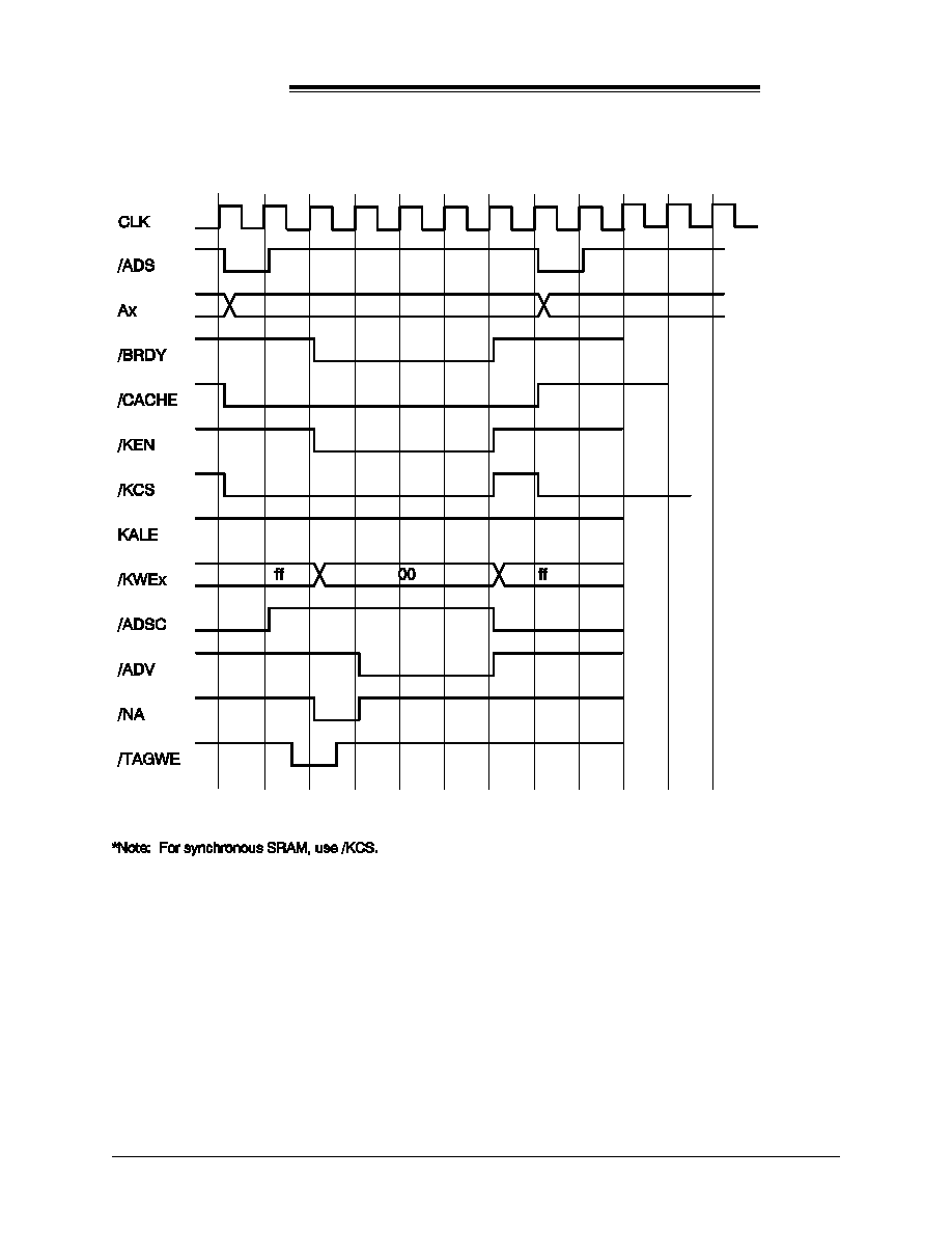
ACC Micro
2051nt
TM
119
6.3.12 Pipeline Synchronous SRAM Burst Write Cycle (3-1-1-1)

ACC Micro
2051nt
TM
120
6.3.13 CPU to PCI Single Read

ACC Micro
2051nt
TM
121
6.3.14 CPU to PCI Single Write, Write to Buffer
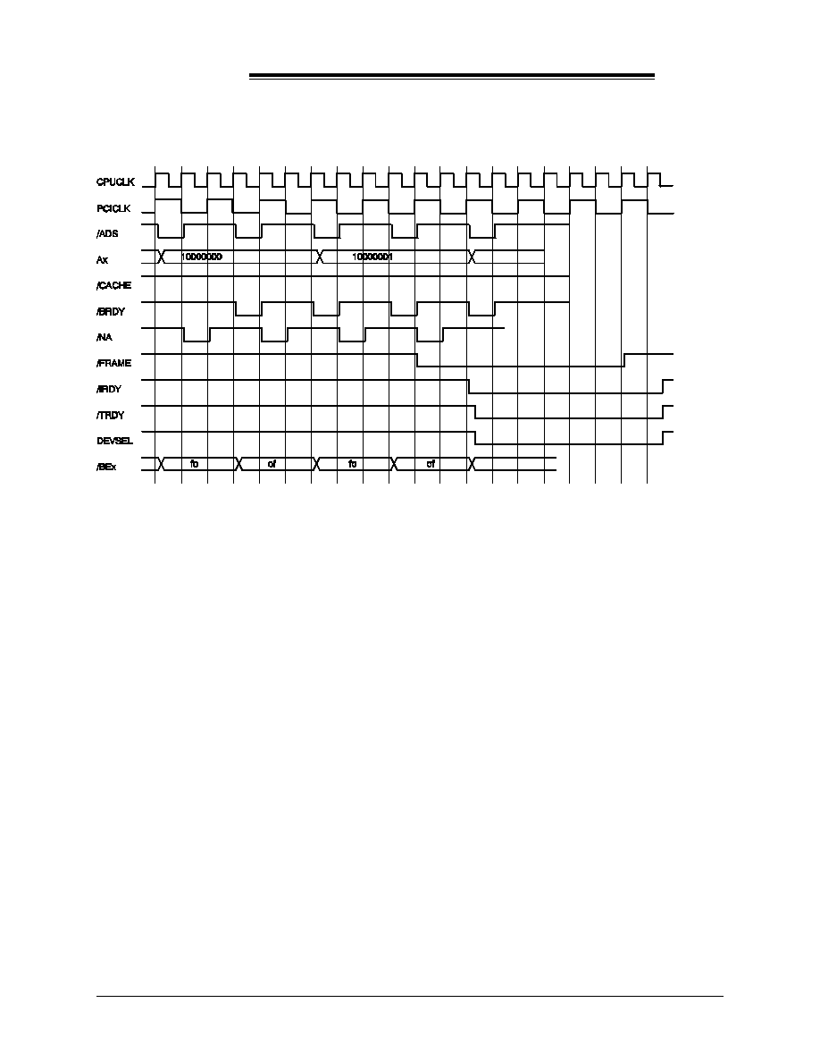
ACC Micro
2051nt
TM
122
6.3.15 CPU to PCI Multiple Write, Write to Buffer, PCI Burst Write

ACC Micro
2051nt
TM
123
Section 7.0
2051nt Pin-out Diagram and Mechanical Data
7.1.1
Pin Side View
Pin A1

ACC Micro
2051nt
TM
124
7.1.2
Top View
Pin A1
The "top view" of the pin diagram above is the view of the ACC Micro 2051nt pin locations as if they
could be looked through from the top of the molding/PCB substrate.

ACC Micro
2051nt
TM
125
7.1.3
Mechanical Data - Top View and Side View
E
He
D
Hd
A1 C
F
Y
A2
Pin A1 Indicator

ACC Micro
2051nt
TM
126
7.1.4
Mechanical Data - Top View
The "top side view" of the pin diagram above is the view of the ACC Micro 2051nt pin locations as if
they could be looked through from the top of the molding/PCB substrate.

ACC Micro
2051nt
TM
127
7.1.5
Package Dimensions
Symbol
Minimum
Typical
Maximum
A1
0.55 mm
0.60 mm
0.65 mm
A2
1.12 mm
1.17 mm
1.22 mm
b
0.60 mm
0.75 mm
0.90 mm
C
0.51 mm
0.56 mm
0.61 mm
D
34.30 mm
34.50 mm
34.70 mm
D1
35.36 mm
35.56 mm
35.76 mm
E
34.30 mm
34.50 mm
34.70 mm
E1
35.36 mm
35.56 mm
35.76 mm
F
4.6*45 (4X)
e
1.27 mm
Hd
37.30 mm
37.50 mm
37.70 mm
He
37.30 mm
37.50 mm
37.70 mm
23�
30�
37�
Y
0.15 mm

Sales Offices
APPENDIX A-1
ACC Microelectronics Headquarters
ACC Microelectronics Corporation
2500 Augustine Drive,
Santa Clara, CA 95054
Phone: (408) 980-0622
Fax: (408) 980-0626
International Sales
Taiwan
ACC Taiwan Inc.
10-2 FL., No.77. Sec.4,
Nan-King E. Rd.,
Taipei, Taiwan, R.O.C.
Phone: (02) 719-9076
Fax: (02) 514-9127
Seper Technology Corp.
4th Fl., 75 Sec. 3,
Ming-Sheng E. Rd.,
Taipei, Taiwan, R.O.C.
Phone: (02) 506-3320
Fax: (02) 504-8081
Yosun Industrial Corporation
7F, No. 76, Sec. 1, Cheng Kung Road
Nan Kang, Taipei, Taiwan
Phone: (02) 788-1991
Fax: (02) 788-1996
Japan
Nippon IMEX Corp.
1-46-9 Matsubara
Setagaya-Ku
Tokyo, 156 Japan
Phone: (33) 321-8000
Fax: (33) 325-0021
Korea
Intellect, Inc.
Sonam Bldg. 3F, 1001-4,
Dacchi-dong, Kangnam-Ku
Seoul, Korea
Phone: (2) 568-0501
Fax: (2) 558-0444
Connecticut
Dynamic Sales
24 Ray Avenue
Burlington, MA 01803
Phone: (617) 272-5676
Fax: (617) 273-4856
Maine
Dynamic Sales
24 Ray Avenue
Burlington, MA 01803
Phone: (617) 272-5676
Fax: (617) 273-4856
Massachusettes
Dynamic Sales
24 Ray Avenue
Burlington, MA 01803
Phone: (617) 272-5676
Fax: (617) 273-4856
Minnesota
D.A. Case Associates, Inc.
4620 West 77th Street #250
Minneapolis, MN 55435
Phone: (612) 831-6777
Fax: (612) 831-7076
New Hampshire
Dynamic Sales
24 Ray Avenue
Burlington, MA 01803
Phone: (617) 272-5676
Fax: (617) 273-4856
North Dakota
D.A. Case Associates, Inc.
4620 West 77th Street #250
Minneapolis, MN 55435
Phone: (612) 831-6777
Fax: (612) 831-7076

Sales Offices
APPENDIX A-1
contd...
Rhode Island
Dynamic Sales
24 Ray Avenue
Burlington, MA 01803
Phone: (617) 272-5676
Fax: (617) 273-4856
South Dakota
D.A. Case Associates, Inc.
4620 West 77th Street #250
Minneapolis, MN 55435
Phone: (612) 831-6777
Fax: (612) 831-7076
Vermont
Dynamic Sales
24 Ray Avenue
Burlington, MA 01803
Phone: (617) 272-5676
Fax: (617) 273-4856
Wisconsin (Western)
D.A. Case Associates, Inc.
4620 West 77th Street #250
Minneapolis, MN 55435
Phone: (612) 831-6777
Fax: (612) 831-7076