
This Data Sheet may be revised by subsequent versions ©2004 Eon Silicon Solution, Inc., www.essi.com.tw
or modifications due to changes in technical specifications.
1
EN29LV160A
Rev. D, Issue Date: 2006/02/24
FEATURES
∑
3.0V, single power supply operation
- Minimizes system level power requirements
∑
High performance
- Access times as fast as 70 ns
∑
Low power consumption (typical values at 5
MHz)
- 9 mA typical active read current
- 20 mA typical program/erase current
- Less than 1
A standby current
∑
Flexible Sector Architecture:
- One 16-Kbyte, two 8-Kbyte, one 32-Kbyte,
and thirty-one 64-Kbyte sectors (byte mode)
- One 8-Kword, two 4-Kword, one 16-Kword
and thirty-one 32-Kword sectors (word mode)
∑
Sector protection :
- Hardware locking of sectors to prevent
program or erase operations within individual
sectors
- Additionally, temporary Sector Group
Unprotect allows code changes in previously
locked sectors.
∑
High performance program/erase speed
- Byte/Word program time: 8µs typical
- Sector erase time: 500ms typical
- Chip erase time: 17.5s typical
∑
JEDEC Standard program and erase
commands
∑
JEDEC standard DATA# polling and toggle
bits feature
∑
Single Sector and Chip Erase
∑
Sector Unprotect Mode
∑
Embedded Erase and Program Algorithms
∑
Erase Suspend / Resume modes:
Read and program another Sector during
Erase Suspend Mode
∑
Triple-metal double-poly triple-well CMOS
Flash Technology
∑
Low Vcc write inhibit < 2.5V
∑
minimum 100K program/erase endurance
cycle
∑
Package Options
- 48-pin TSOP (Type 1)
- 48 ball 6mm x 8mm FBGA
∑
Commercial and Industrial Temperature
Range
GENERAL DESCRIPTION
The EN29LV160A is a 16-Megabit, electrically erasable, read/write non-volatile flash memory,
organized as 2,097,152 bytes or 1,048,576 words. Any byte can be programmed typically in 8µs.
The EN29LV160A features 3.0V voltage read and write operation, with access times as fast as
70ns to eliminate the need for WAIT states in high-performance microprocessor systems.
The EN29LV160A has separate Output Enable (OE#), Chip Enable (CE#), and Write Enable
(WE#) controls, which eliminate bus contention issues. This device is designed to allow either
single
Sector or full chip erase operation, where each Sector can be individually protected
against program/erase operations or temporarily unprotected to erase or program. The device
can sustain a minimum of 100K program/erase cycles on each Sector.
.
EN29LV160A
16 Megabit (2048K x 8-bit / 1024K x 16-bit) Flash Memory
Boot Sector Flash Memory, CMOS 3.0 Volt-only

This Data Sheet may be revised by subsequent versions ©2004 Eon Silicon Solution, Inc., www.essi.com.tw
or modifications due to changes in technical specifications.
2
EN29LV160A
Rev. D, Issue Date: 2006/02/24
CONNECTION DIAGRAMS
A6
A5
A4
A1
A3
A2
FBGA
Top View, Balls Facing Down
A13
A9
A3
RY/BY#
WE#
A7
B6
B5
B4
B1
B3
B2
A12
A8
A4
NC
RESET#
A17
C6
C5
C4
C1
C3
C2
A14
A10
A2
A18
NC
A6
D6
D5
D4
D1
D3
D2
A15
A11
A1
NC
A19
A5
E6
E5
E4
E1
E3
E2
A16
DQ7
A0
DQ2
DQ5
DQ0
F6
F5
F4
F3
F2
BYTE#
DQ14
CE#
DQ10
DQ12
DQ8
G6
G5
G4
G3
G2
DQ15/A-1
DQ13
OE#
DQ11
Vcc
DQ9
H6
H5
H3
H2
Vss
DQ6
Vss
DQ4
DQ1
F1
G1
H4
H1
DQ3
1
2
3
4
5
6
7
8
9
10
11
12
13
14
15
16
17
18
19
20
21
22
23
24
48
47
46
45
44
43
42
41
40
39
38
37
36
35
34
33
32
31
30
29
28
27
26
25
Standard
TSOP
A15
A14
A13
A12
A11
A10
A9
A8
A19
NC
WE#
RESET#
NC
NC
RY/BY#
A18
A17
A7
A6
A5
A4
A3
A2
A1
A16
BYTE#
Vss
DQ15/A-1
DQ7
DQ14
DQ6
DQ13
DQ5
DQ12
DQ4
Vcc
DQ11
DQ3
DQ10
DQ2
DQ9
DQ1
DQ8
DQ0
OE#
Vss
CE#
A0
This Data Sheet may be revised by subsequent versions ©2004 Eon Silicon Solution, Inc., www.essi.com.tw
or modifications due to changes in technical specifications.
3
EN29LV160A
Rev. D, Issue Date: 2006/02/24
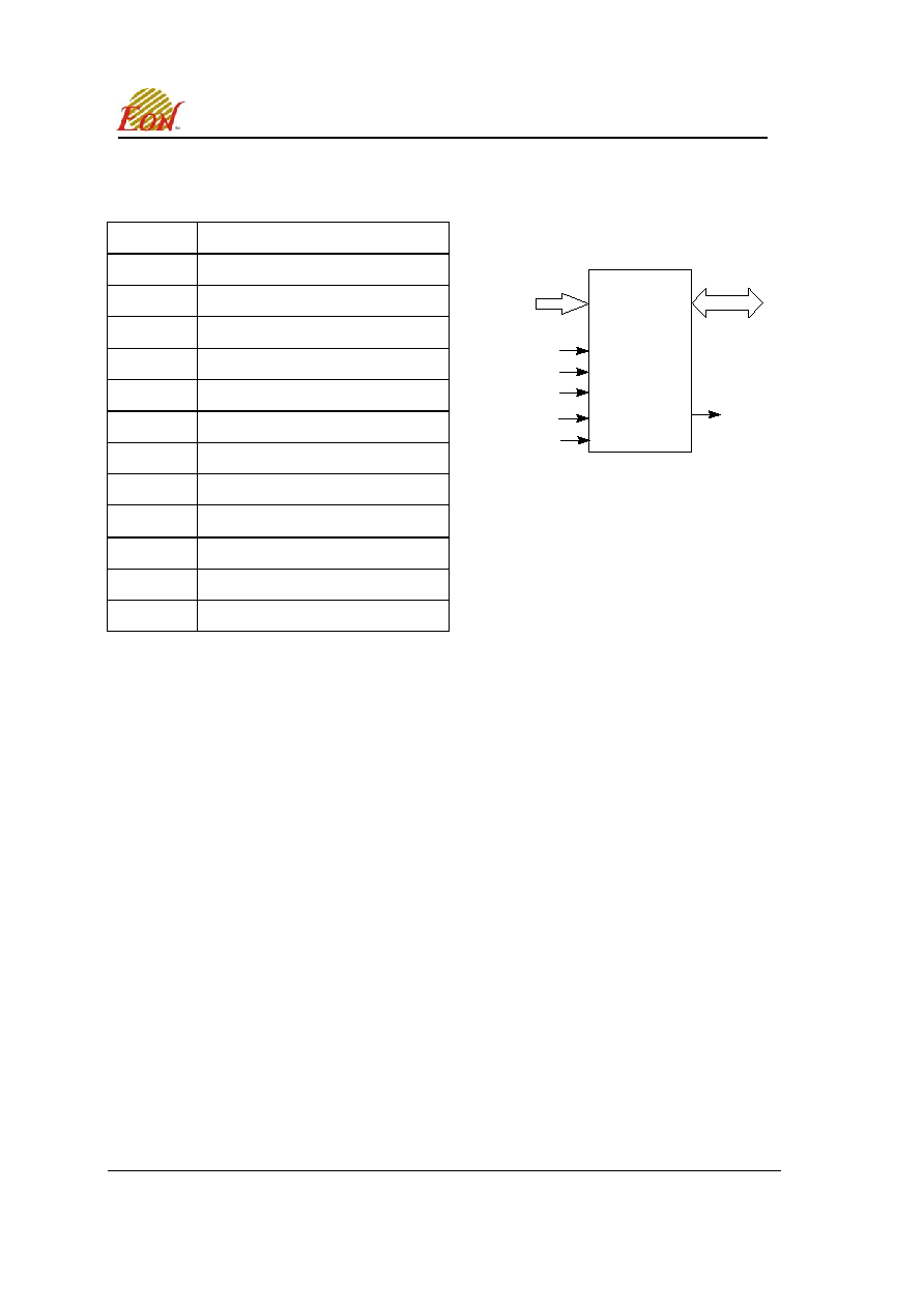
TABLE 1. PIN DESCRIPTION
FIGURE 1. LOGIC DIAGRAM
Pin Name
Function
A0-A19 20
Addresses
DQ0-DQ14
15 Data Inputs/Outputs
DQ15 / A-1
DQ15 (data input/output, word mode),
A-1 (LSB address input, byte mode)
CE# Chip
Enable
OE# Output
Enable
RESET#
Hardware Reset Pin
RY/BY# Ready/Busy
Output
WE# Write
Enable
Vcc
Supply Voltage
(2.7-3.6V)
Vss Ground
NC
Not Connected to anything
BYTE# Byte/Word
Mode
EN29LV160A
DQ0 ≠ DQ15
(A-1)
A0 ≠ A19
WE#
CE#
RY/BY#
Reset#
Byte#
OE#

This Data Sheet may be revised by subsequent versions ©2004 Eon Silicon Solution, Inc., www.essi.com.tw
or modifications due to changes in technical specifications.
4
EN29LV160A
Rev. D, Issue Date: 2006/02/24
Table 2. Top Boot Sector Address Tables (EN29LV160AT)
Address Range (in hexadecimal)
Sector A19 A18 A17 A16 A15 A14
A13
A12
Sector Size
(Kbytes/
Kwords)
Byte mode (x8)
Word Mode
(x16)
SA0 0 0 0 0 0 X X X 64/32 000000≠00FFFF 00000≠07FFF
SA1 0 0 0 0 1 X X X 64/32 010000≠01FFFF 08000≠0FFFF
SA2 0 0 0 1 0 X X X 64/32 020000≠02FFFF 10000≠17FFF
SA3 0 0 0 1 1 X X X 64/32 030000≠03FFFF 18000≠1FFFF
SA4 0 0 1 0 0 X X X 64/32 040000≠04FFFF 20000≠27FFF
SA5 0 0 1 0 1 X X X 64/32 050000≠05FFFF 28000≠2FFFF
SA6 0 0 1 1 0 X X X 64/32 060000≠06FFFF 30000≠37FFF
SA7 0 0 1 1 1 X X X 64/32 070000≠07FFFF 38000≠3FFFF
SA8 0 1 0 0 0 X X X 64/32 080000≠08FFFF 40000≠47FFF
SA9 0 1 0 0 1 X X X 64/32 090000≠09FFFF 48000≠4FFFF
SA10 0 1 0 1 0 X X X 64/32 0A0000≠0AFFFF
50000≠57FFF
SA11 0 1 0 1 1 X X X 64/32 0B0000≠0BFFFF
58000≠5FFFF
SA12 0 1 1 0 0 X X X 64/32 0C0000≠0CFFFF
60000≠67FFF
SA13 0 1 1 0 1 X X X 64/32 0D0000≠0DFFFF
68000≠6FFFF
SA14 0 1 1 1 0 X X X 64/32 0E0000≠0EFFFF
70000≠77FFF
SA15 0 1 1 1 1 X X X 64/32 0F0000≠0FFFFF
78000≠7FFFF
SA16 1 0 0 0 0 X X X 64/32 100000≠10FFFF 80000≠87FFF
SA17 1 0 0 0 1 X X X 64/32 110000≠11FFFF 88000≠8FFFF
SA18 1 0 0 1 0 X X X 64/32 120000≠12FFFF 90000≠97FFF
SA19 1 0 0 1 1 X X X 64/32 130000≠13FFFF 98000≠9FFFF
SA20 1 0 1 0 0 X X X 64/32 140000≠14FFFF
A0000≠A7FFF
SA21 1 0 1 0 1 X X X 64/32 150000≠15FFFF
A8000≠AFFFF
SA22 1 0 1 1 0 X X X 64/32 160000≠16FFFF
B0000≠B7FFF
SA23 1 0 1 1 1 X X X 64/32 170000≠17FFFF
B8000≠BFFFF
SA24 1 1 0 0 0 X X X 64/32 180000≠18FFFF
C0000≠C7FFF
SA25 1 1 0 0 1 X X X 64/32 190000≠19FFFF
C8000≠CFFFF
SA26 1 1 0 1 0 X X X 64/32 1A0000≠1AFFFF
D0000≠D7FFF
SA27 1 1 0 1 1 X X X 64/32 1B0000≠1BFFFF
D8000≠DFFFF
SA28 1 1 1 0 0 X X X 64/32 1C0000≠1CFFFF
E0000≠E7FFF
SA29 1 1 1 0 1 X X X 64/32 1D0000≠1DFFFF
E8000≠EFFFF
SA30 1 1 1 1 0 X X X 64/32 1E0000≠1EFFFF
F0000≠F7FFF
SA31 1 1 1 1 1 0 X X 32/16 1F0000≠1F7FFF
F8000≠FBFFF
SA32 1 1 1 1 1 1 0 0
8/4
1F8000≠1F9FFF
FC000≠FCFFF
SA33 1 1 1 1 1 1 0 1
8/4 1FA000≠1FBFFF
FD000≠FDFFF
SA34 1 1 1 1 1 1 1 X
16/8 1FC000≠1FFFFF
FE000≠FFFFF

This Data Sheet may be revised by subsequent versions ©2004 Eon Silicon Solution, Inc., www.essi.com.tw
or modifications due to changes in technical specifications.
5
EN29LV160A
Rev. D, Issue Date: 2006/02/24
Table 3. Bottom Boot Sector Address Tables (EN29LV160AB)
Address Range (in hexadecimal)
Sector A19 A18 A17 A16 A15 A14
A13
A12
Sector Size
(Kbytes/
Kwords)
Byte mode (x8)
Word Mode
(x16)
SA0 0 0 0 0 0 0 0 X
16/8 000000≠003FFF 00000≠01FFF
SA1 0 0 0 0 0 0 1 0
8/4
004000≠005FFF 02000≠02FFF
SA2 0 0 0 0 0 0 1 1
8/4
006000≠007FFF 03000≠03FFF
SA3 0 0 0 0 0 1 X X 32/16 008000≠00FFFF 04000≠07FFF
SA4 0 0 0 0 1 X X X 64/32 010000≠01FFFF 08000≠0FFFF
SA5 0 0 0 1 0 X X X 64/32
020000≠02FFFF 10000≠17FFF
SA6 0 0 0 1 1 X X X 64/32
030000≠03FFFF 18000≠1FFFF
SA7 0 0 1 0 0 X X X 64/32
040000≠04FFFF 20000≠27FFF
SA8 0 0 1 0 1 X X X 64/32
050000≠05FFFF 28000≠2FFFF
SA9 0 0 1 1 0 X X X 64/32
060000≠06FFFF 30000≠37FFF
SA10 0 0 1 1 1 X X X 64/32
070000≠07FFFF 38000≠3FFFF
SA11 0 1 0 0 0 X X X 64/32
080000≠08FFFF 40000≠47FFF
SA12 0 1 0 0 1 X X X 64/32
090000≠09FFFF 48000≠4FFFF
SA13 0 1 0 1 0 X X X 64/32
0A0000≠0AFFFF 50000≠57FFF
SA14 0 1 0 1 1 X X X 64/32
0B0000≠0BFFFF
58000≠5FFFF
SA15 0 1 1 0 0 X X X 64/32
0C0000≠0CFFFF 60000≠67FFF
SA16 0 1 1 0 1 X X X 64/32
0D0000≠0DFFFF 68000≠6FFFF
SA17 0 1 1 1 0 X X X 64/32
0E0000≠0EFFFF 70000≠77FFF
SA18 0 1 1 1 1 X X X 64/32
0F0000≠0FFFFF 78000≠7FFFF
SA19 1 0 0 0 0 X X X 64/32
100000≠10FFFF 80000≠87FFF
SA20 1 0 0 0 1 X X X 64/32
110000≠11FFFF 88000≠8FFFF
SA21 1 0 0 1 0 X X X 64/32
120000≠12FFFF 90000≠97FFF
SA22 1 0 0 1 1 X X X 64/32
130000≠13FFFF 98000≠9FFFF
SA23 1 0 1 0 0 X X X 64/32
140000≠14FFFF A0000≠A7FFF
SA24 1 0 1 0 1 X X X 64/32
150000≠15FFFF A8000≠AFFFF
SA25 1 0 1 1 0 X X X 64/32
160000≠16FFFF B0000≠B7FFF
SA26 1 0 1 1 1 X X X 64/32
170000≠17FFFF B8000≠BFFFF
SA27 1 1 0 0 0 X X X 64/32
180000≠18FFFF C0000≠C7FFF
SA28 1 1 0 0 1 X X X 64/32
190000≠19FFFF C8000≠CFFFF
SA29 1 1 0 1 0 X X X 64/32
1A0000≠1AFFFF D0000≠D7FFF
SA30 1 1 0 1 1 X X X 64/32
1B0000≠1BFFFF D8000≠DFFFF
SA31 1 1 1 0 0 X X X 64/32
1C0000≠1CFFFF E0000≠E7FFF
SA32 1 1 1 0 1 X X X 64/32
1D0000≠1DFFFF E8000≠EFFFF
SA33 1 1 1 1 0 X X X 64/32
1E0000≠1EFFFF F0000≠F7FFF
SA34 1 1 1 1 1 X X X 64/32
1F0000≠1FFFFF F8000≠FFFFF