Note: All information contained in this data sheet has been carefully checked and is believed to be accurate as of the date of publication; however, this data sheet cannot be a "controlled document". Current revisions, if any, to these
specifications are maintained at the factory and are available upon your request. We recommend checking the revision level before finalization of your design documentation.
© 2001 Elantec Semiconductor, Inc.
E
L
4
0
0
C
General Description
The EL400C is a wide bandwidth, fast settling monolithic amplifier
built using an advanced complementary bipolar process. This ampli-
fier uses current-mode feedback to achieve more bandwidth at a given
gain than conventional operational amplifiers. Designed for closed-
loop gains of ±1 to ±8, the EL400C has a 200MHz -3dB bandwidth
(A
V
= +2), and 12ns settling to 0.05% while consuming only 15mA of
supply current.
The EL400C is an obvious high-performance solution for video distri-
bution and line-driving applications. With low 15mA supply current,
differential gain/phase of 0.02%/0.01∞, and a minimum 50mA output
drive, performance in these areas is assured.
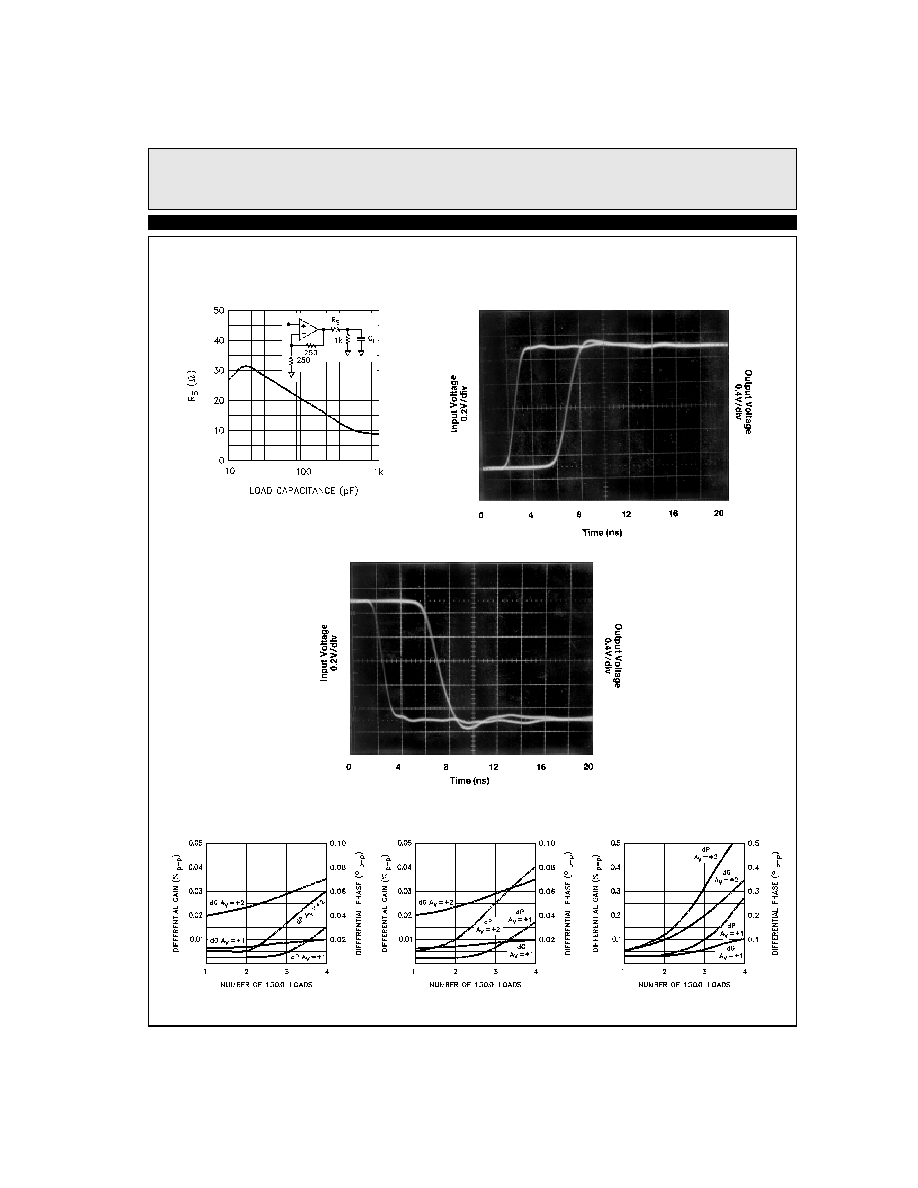
The EL400's settling to 0.05% in 12ns, low distortion, and ability to
drive capacitive loads make it an ideal flash A/D driver. The wide
200MHz bandwidth and extremely linear phase allow unmatched sig-
nal fidelity. D/A systems can also benefit from the EL400C, especially
if linearity and drive levels are important.
Connection Diagrams
DIP and SO Package
Top View
Manufactured under U.S. Patent No. 4,893,091
Features
∑ 200MHz -3dB bandwidth, A
V
= 2
∑ 12ns settling to 0.05%
∑ V
S
= ±5V @ 15mA
∑ Low distortion: HD2, HD3 @
-60dBc at 20MHz
∑ Differential gain 0.02% at NTSC,
PAL
∑ Differential phase 0.01∞ at NTSC,
PAL
∑ Overload/short-circuit protected
∑ ±1 to ±8 closed-loop gain range
∑ Low cost
∑ Direct replacement for CLC400
Applications
∑ Video gain block
∑ Video distribution
∑ HDTV amplifier
∑ High-speed A/D conversion
∑ D/A I-V conversion
∑ Photodiode, CCD preamps
∑ IF processors
∑ High-speed communications
Ordering Information
Part No.
Temp. Range
Package
Outline #
EL400CN
-40∞C to +85∞C
8-Pin P-DIP
MDP0031
EL400CS
-40∞C to +85∞C
8-Lead SO
MDP0027
EL400C
200MHz Current Feedback Amplifier
S
e
p
t
e
m
b
e
r
2
6
,
2
0
0
1
2
EL400C
200MHz Current Feedback Amplifier
E
L
4
0
0
C
Absolute Maximum Ratings
(T
A
= 25∞C)
Supply Voltage (V
S
)
±7V
Output Current
Output is short-circuit protected to ground, however, maximum reliability is obtained if
I
OUT
does not exceed 70mA.
Common-Mode Input Voltage
±V
S
Differential Input Voltage
5V
Power Dissipation
See Curves
Operating Temperature
-40∞C to +85∞C
Lead Temperature (Soldering, 5 Seconds)
300∞C
Junction Temperature
175∞C
Storage Temperature
-60∞C to +150∞C
Thermal Resistance:
JA
= 95∞C/W P-DIP
JA
= 175∞C/W SO-8
Important Note:
All parameters having Min/Max specifications are guaranteed. Typ values are for information purposes only. Unless otherwise noted, all tests are at the
specified temperature and are pulsed tests, therefore: T
J
= T
C
= T
A
.
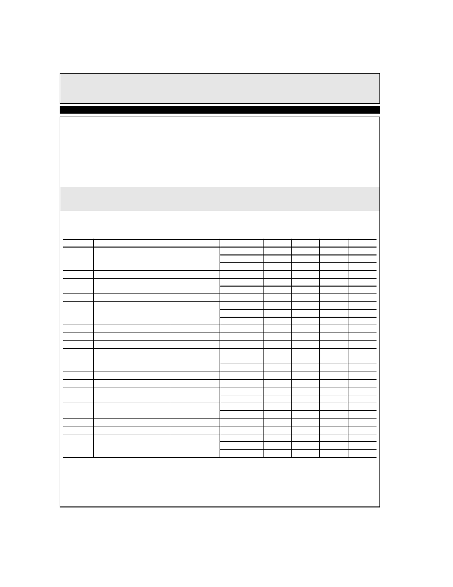
Open Loop DC Electrical Characteristics
V
S
= ±5V, R
L
= 100
unless otherwise specified
Parameter
Description
Test Conditions
Temp
Min
Typ
Max
Unit
V
OS
Input Offset Voltage
25∞C
2.0
5.5
mV
T
MIN
8.7
mV
T
MAX
9.5
mV
d(V
OS
)/dT
Average Offset Voltage Drift
[1]
All
10.0
40.0
µV/∞C
+I
IN
+Input Current
25∞C, T
MAX
10.0
25.0
µA
T
MIN
41.0
µA
d(+I
IN
)/dT
Average +Input Current Drift
[1]
All
50.0
200.0
nA/∞C
-I
IN
-Input Current
25∞C
10.0
25.0
µA
T
MIN
41.0
µA
T
MAX
35.0
µA
d(-I
IN
)/dT
Average -Input Current Drift
[1]
All
100.0
200.0
nA/∞C
PSRR
Power Supply Rejection Ratio
All
40.0
50.0
dB
CMRR
Common-Mode Rejection Ratio
All
40.0
50.0
dB
I
S
Supply Current--Quiescent
No Load
All
15.0
23.0
mA
+R
IN
+Input Resistance
25∞C, T
MAX
100.0
200.0
k
T
MIN
50.0
k
C
IN
Input Capacitance
All
0.5
2.0
pF
R
OUT
Output Impedance (DC)
All
0.1
0.2
CMIR
Common-Mode Input Range
[2]
25∞C, T
MAX
2.0
2.1
V
T
MIN
1.2
V
I
OUT
Output Current
25∞C, T
MAX
50.0
70.0
mA
T
MIN
35.0
mA
V
OUT
Output Voltage Swing
No Load
All
3.2
3.5
V
V
OUTL
Output Voltage Swing
100
25∞C
3.0
3.4
V
R
OL
Transimpedance
25∞C
30.0
125.0
V/mA
T
MIN
80.0
V/mA
T
MAX
140.0
V/mA
1. Measured from T
MIN
to T
MAX
.
2. Common-Mode Input Range for Rated Performance.

3
EL400C
200MHz Current Feedback Amplifier
E
L
4
0
0
C
Closed-Loop AC Electrical Characteristics
V
S
= ±5V, R
F
= 250
, A
V
= +2, R
L
= 100
unless otherwise specified
Parameter
Description
Test Conditions
Temp
Min
Typ
Max
Unit
Frequency
Response
SSBW -3dB Bandwidth
(V
OUT
< 0.5V
PP
)
25∞C
150.0
200.0
MHz
T
MIN
150.0
MHz
T
MAX
120.0
MHz
LSBW -3dB Bandwidth
(V
OUT
< 5.0V
PP
)
A
V
= +5
All
35.0
50.0
MHz
Gain Flatness
GFPL
Peaking
V
OUT
< 0.5V
PP
<40MHz
25∞C
0.0
0.3
dB
T
MIN
, T
MAX
0.4
dB
GFPH
Peaking
V
OUT
< 0.5V
PP
>40MHz
25∞C
0.0
0.5
dB
T
MIN
, T
MAX
0.7
dB
GFR
Rolloff
V
OUT
< 0.5V
PP
<75MHz
25∞C
0.6
1.0
dB
T
MIN
1.0
dB
T
MAX
1.3
dB
LPD
Linear Phase Deviation
V
OUT
< 0.5V
PP
<75MHz
25∞C, T
MIN
0.2
1.0
∞
T
MAX
1.2
∞
Time-Domain
Response
t
r1
, t
f1
Rise Time, Fall Time
0.5V Step
25∞C, T
MIN
1.6
2.4
ns
T
MAX
2.9
ns
t
r2
, t
f2
Rise Time, Fall Time
5.0V Step
All
6.5
10.0
ns
t
s1
Settling Time to 0.1%
2.0V Step
All
10.0
13.0
ns
t
s2
Settling Time to 0.05%
2.0V Step
All
12.0
15.0
ns
OS
Overshoot
0.5V Step
25∞C
0.0
10.0
%
T
MIN
, T
MAX
15.0
%
SR
Slew Rate
A
V
= +2
All
430.0
700.0
V/µs
A
V
= - 2
All
1600.0
V/µs
Distortion
HD2
2nd Harmonic Distortion at 20MHz
2V
PP
25∞C
-60.0
-45.0
dBc
T
MIN
-40.0
dBc
T
MAX
-45.0
dBc
HD3
3rd Harmonic Distortion at 20MHz
2V
PP
25∞C
-60.0
-50.0
dBc
T
MIN
, T
MAX
-50.0
dBc
Equivalent Input
Noise
NF
Noise Floor
>100kHz
[1]
25∞C
-157.0
-154.0
dBm
(1Hz)
T
MIN
-154.0
dBm
(1Hz)
T
MAX
-153.0
dBm
(1Hz)
INV
Integrated Noise
100kHz to 200MHz
[1]
25∞C
40.0
57.0
µV
T
MIN
57.0
µV
T
MAX
63.0
µV
Video
Performance
d
G
Differential Gain
[2]
NTSC/PAL
25∞C
0.02
% pp
d
P
Differential Phase
[2]
NTSC/PAL
25∞C
0.01
∞ pp
d
G
Differential Gain
[2]
30MHz
25∞C
0.05
% pp
d
P
Differential Phase
[2]
30MHz
25∞C
0.05
∞ pp
VBW
-0.1dB Bandwidth
[2]
25∞C
60.0
MHz
1. Noise Tests are Performed from 5MHz to 200MHz.
2. Differential Gain/Phase Tests are R
L
= 100
. For other values of R
L
, see curves.
4
EL400C
200MHz Current Feedback Amplifier
E
L
4
0
0
C
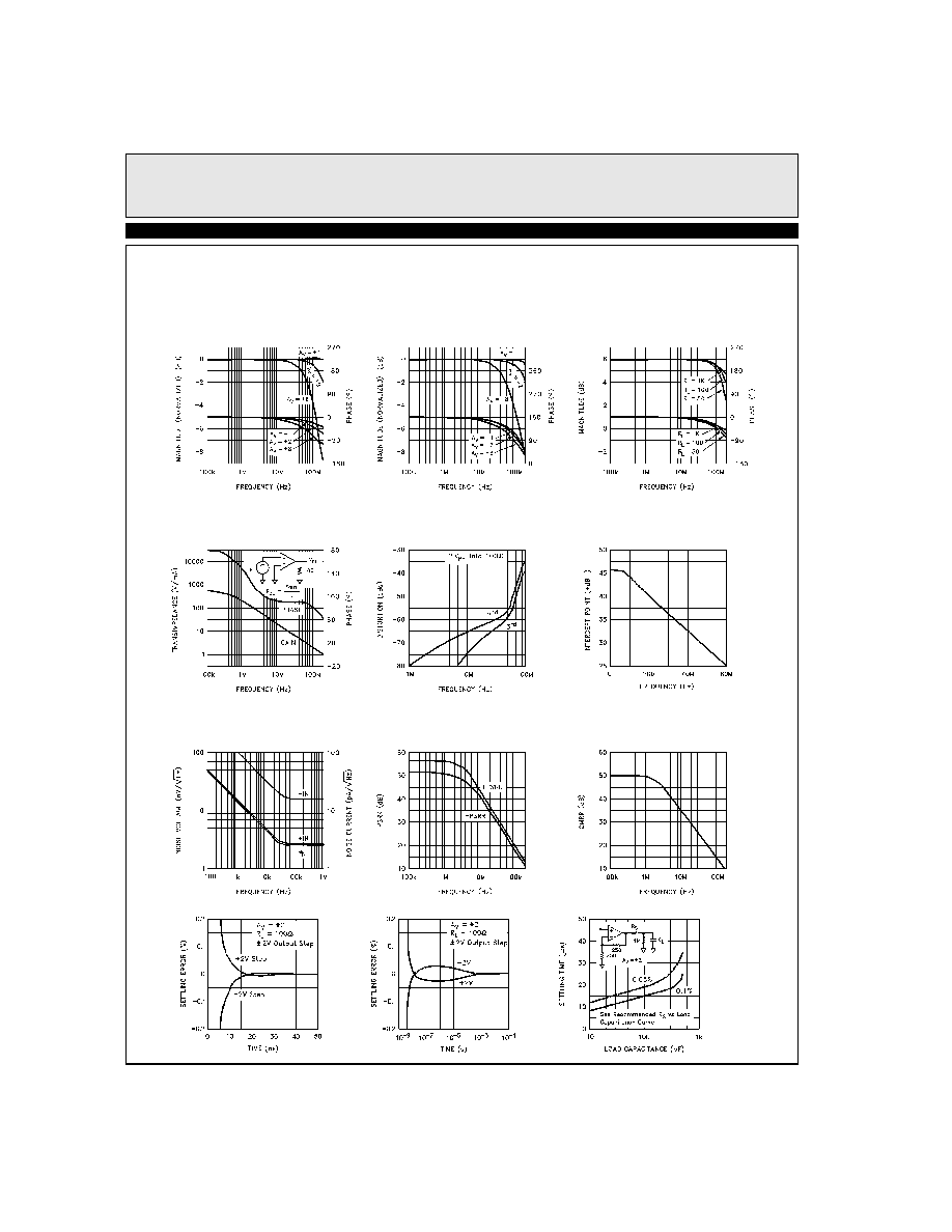
Typical Performance Curves
Non-Inverting
Frequency Response
Inverting Frequency Response
Frequency Response for
Various R
L
s
Open-Loop Transimpedance
Gain and Phase
2nd and 3rd
Harmonic Distortion
2-Tone 3rd Order
Intermodulation Intercept
Equivalent Input Noise
Power-Supply
Rejection Ratio
Common-Mode
Rejection Ratio
Settling Time
Long-Term Settling Time
Settling Time vs Load Capacitance