 | ÐлекÑÑоннÑй компоненÑ: DS2740 | СкаÑаÑÑ:  PDF PDF  ZIP ZIP |
Äîêóìåíòàöèÿ è îïèñàíèÿ www.docs.chipfind.ru
1 of 15
033103
FEATURES
§ 15-Bit Bidirectional Current Measurement
(DS2740)
§ 1.56mV LSB and ±51.2mV Dynamic
Range
§ 78mA LSB and ±2.56A Dynamic
Range with External 20m
W Sense
Resistor (R
SNS
)
§ 156mA LSB and ±5.12A Dynamic
Range with External 10m
W Sense
Resistor (R
SNS
)
§ 13-Bit Bidirectional Current Measurement
(DS2740B)
§ 6.25mV LSB and ±51.2mV Dynamic
Range
§ 312mA LSB and ±2.56A Dynamic
Range with External 20m
W Sense
Resistor (R
SNS
)
§ 625mA LSB and ±5.12A Dynamic
Range with External 10m
W Sense
Resistor (R
SNS
)
§ Analog Input Filter (IS1, IS2) Extends
Dynamic Range for Pulse-Load
Applications
§ Current Accumulation Register
Resolution
§ 6.25mVhr (Both DS2740 and
DS2740B)
§ 0.3125mAhr with External 20mW
R
SNS
§ 0.6250mAhr with External 10mW
R
SNS
§ Dallas 1-Wire
®
Interface
§ Unique 64-Bit Device Address
§ Standard and Overdrive Timings
(OVD)
§ Low Power Consumption:
§ Active Current: 65mA max
§ Sleep Current: 1mA max
PIN CONFIGURATION
PIN DESCRIPTION
OVD- 1-Wire Bus Speed Select
PIO - Programmable I/O Pin
SNS - Sense Resistor Input
IS2 - Current-Sense Input
IS1 - Current-Sense Input
V
SS
- Device Ground, Current-Sense Resistor
Return
DQ - Data Input/Output
V
DD
- Power-Supply Input (2.7V to 5.5V)
DS2740
High-Precision Coulomb Counter
www.maxim-ic.com
mMAX
(DS2740U, DS2740BU)
PIO
V
DD
DQ
V
SS
IS1
IS2
SNS
OVD
6
8
7
5
3
1
2
4
See Table 1 for Ordering Information.
See Table 2 for Detailed Pin Descriptions.
1-Wire is a registered trademark of Dallas Semiconductor.
DS2740
2 of 15
Table 1.
ORDERING INFORMATION
PART
MARKING
PIN-PACKAGE
DS2740U
DS2740
15-Bit Current Resolution,
mMAX
DS2740U/T&R
DS2740
15-Bit Current Resolution,
mMAX, Tape-and-Reel
DS2740BU
DS2740B
13-Bit Current Resolution,
mMAX
DS2740BU/T&R
DS2740B
13-Bit Current Resolution,
mMAX, Tape-and-Reel
DESCRIPTION
The DS2740 provides high-precision current-flow measurement data to support battery-capacity
monitoring in cost-sensitive applications. Current is measured bidirectionally over a dynamic range of 15
bits (DS2740U) or 13 bits (DS2740UB), with the net flow accumulated in a separate 16-bit register.
Through its 1-Wire interface, the DS2740 allows the host system read/write access to status and current
measurement registers. Each device has a unique factory-programmed 64-bit net address that allows it to
be individually addressed by the host system, supporting multibattery slot operation. The interface can be
operated with standard or overdrive timing.
Although the DS2740 is primarily intended for location on the host system, it is also suited for mounting
in the battery pack. The DS2740 and FuelPackTM algorithms, along with host measurements of
temperature and voltage, form a complete and accurate solution for estimating remaining capacity.
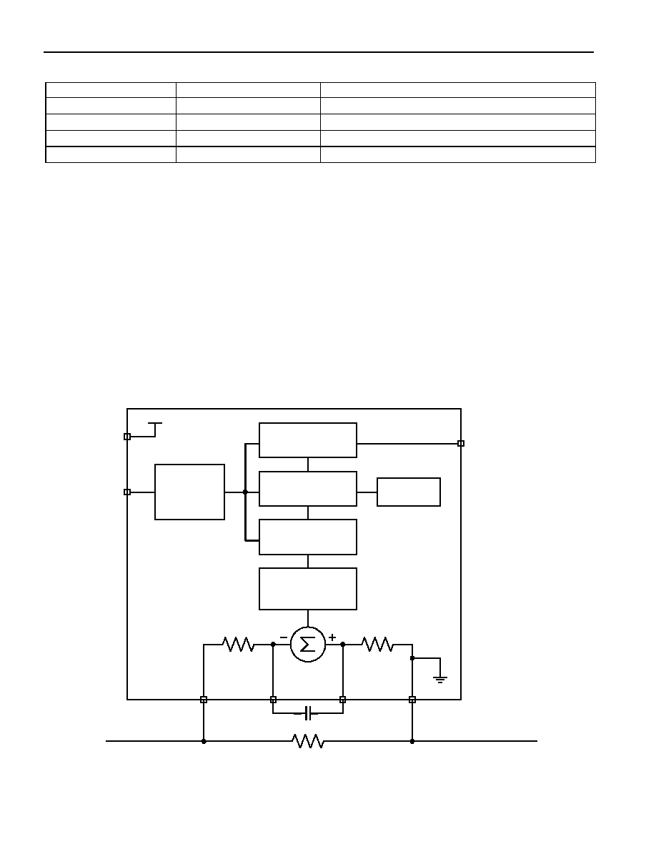
Figure 1. BLOCK DIAGRAM
1-WIRE
INTERFACE
AND
ADDRESS
DQ
PIO
TIMEBASE
CURRENT
ACCUMULATED
CURRENT
STATUS/CONTROL
CHIP
GROUND
SNS
IS2
V
SS
IS1
15-Bit + Sign
ADC
R
IS
10 k
W
R
IS
10 k
W
V
DD
FuelPack is a trademark of Dallas Semiconductor.
DS2740
3 of 15
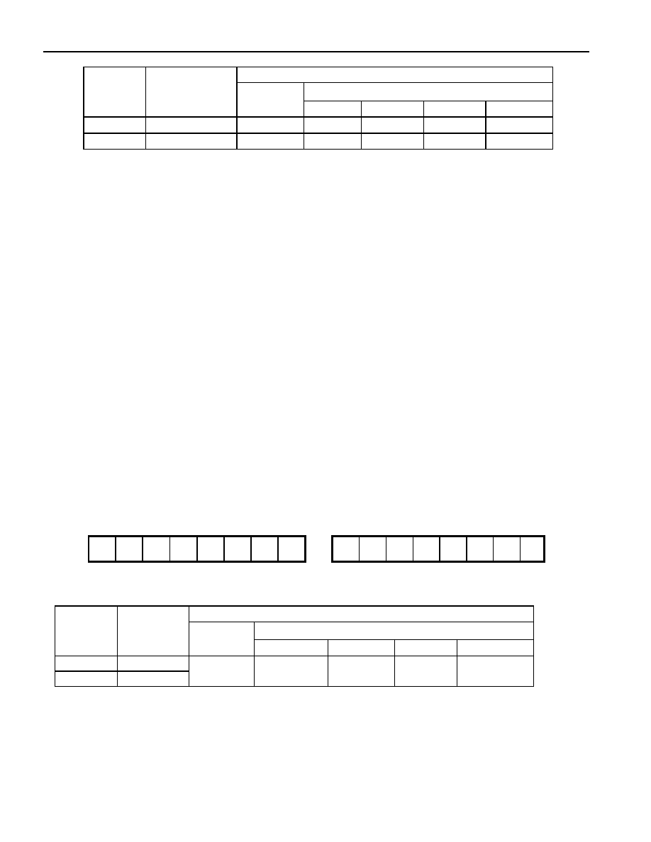
Table 2. DETAILED PIN DESCRIPTION
PIN
SYMBOL
DESCRIPTION
OVD
1
1-Wire Bus Speed Control. Input logic level selects the speed of the 1-
Wire bus. Logic 1 selects overdrive (OVD) and Logic 0 selects standard
timing (STD). On a multidrop bus, all devices must operate at same
speed.
PIO
2
Programmable I/O Pin. Programmed as input or output through internal
registers. Open-drain output sufficient for LED or vibrator activation.
SNS
3
Current-Sense Resistor Input
IS2
4
Current-Sense Input. Connected to SNS through a 10k resistor to
allow filtering of the current waveform by an external capacitor.
IS1
5
Current-Sense Input. Connected to V
SS
through a 10k resistor to allow
filtering of the current waveform through an external capacitor.
V
SS
6
Device Ground, Current-Sense Resistor Return. Connect directly to
the negative terminal of the battery cell.
DQ
7
Data I/O Pin. Operates bidirectionally with open-drain output driver.
Internal 1µA pulldown aids in sensing pack removal and sleep-mode
activation.
V
DD
8
Power-Supply Input. Connects to system voltage supply or positive
terminal of battery cell.
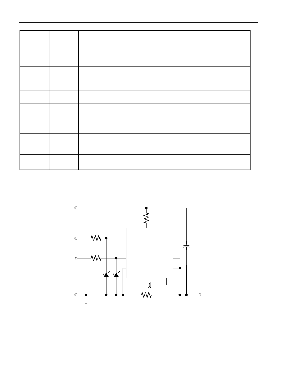
Figure 2. APPLICATION EXAMPLE
DS2740
VDD
VSS
DQ
PIO
DATA
2.7V to 5.5V
System Supply
Battery Pack
Negative
Battery
Pack
Return
SNS
PIO
IS1
IS2
104
150
150
R
SNS
104
System
GND
OVD
*
*
* 5.6V zener recommended for ESD protection when DATA or PIO
contacts exposed, such as a removable battery pack application
150

DS2740
4 of 15
POWER MODES
The DS2740 has two power modes: active and sleep. While in active mode, the DS2740 operates as a
high-precision coulomb counter with current and accumulated current measurement blocks operating
continuously and the resulting values updated in the measurement registers. Read and write access is
allowed to all registers. PIO pin is active. In sleep mode, the DS2740 operates in a low-power mode with
no current measurement activity. Serial access to current, accumulated current, and status/control
registers is allowed if V
DD
> 2V.
The DS2740 operating mode transitions from SLEEP to ACTIVE when:
1)
DQ > V
IH
, and V
DD
> UV threshold, or
2)
V
DD
rises from below UV threshold to above UV threshold.
The DS2740 operating mode transitions from ACTIVE to SLEEP when:
1)
V
DD
falls to UV threshold, or
2)
SMOD = 1 and DQ < V
IL
for 2s.
CURRENT MEASUREMENT
In the active mode of operation, the DS2740 continually measures the current flow into and out of the
battery by measuring the voltage drop across a low-value current-sense resistor, R
SNS
. To extend the input
range for pulse-type load currents, the voltage signal can be filtered by adding a capacitor between the
IS1 and IS2 pins. The external capacitor and two internal resistors form a lowpass filter at the input of the
ADC. The voltage-sense range at IS1 and IS2 is ±51.2mV. The input converts peak signal amplitudes up
to 75mV as long as the continuous or average signal level (post filter) does not exceed ±51.2mV over the
conversion cycle period. The ADC samples the input differentially at IS1 and IS2 with an 18.6kHz
sample clock and updates the current register at the completion of each conversion cycle. Conversion
times for each resolution option are listed in the tables below. Two resolution options are available.
Figure 3 describes the current measurement register format and resolution for each option. "S" indicates
the sign bit(s).
Figure 3. CURRENT REGISTER FORMATS
DS2740: 15-bit + sign resolution, 3.5s conversion period.
MSB--Address 0E
LSB--Address 0F
S
2
14
2
13
2
12
2
11
2
10
2
9
2
8
2
7
2
6
2
5
2
4
2
3
2
2
2
1
2
0
MSb
LSb
MSb
LSb
Units: 1.5625
mV/Rsns
DS2740B: 13-bit + sign resolution, 0.875s conversion period.
MSB--Address 0E
LSB--Address 0F
S
S
S
2
12
2
11
2
10
2
9
2
8
2
7
2
6
2
5
2
4
2
3
2
2
2
1
2
0
MSb
LSb
MSb
LSb
Units: 6.250
mV/Rsns
DS2740
5 of 15
CURRENT RESOLUTION (1 LSB)
R
SNS
PART
CONVERSION
TIME
V
IS1
- V
IS2
20m
W
15m
W
10m
W
5m
W
DS2740
3.515s
1.5625
mV 78.13mA 104.2mA
156.3
mA
312.5
mA
DS2740B
0.878s
6.250
mV
312.5
mA 416.7mA
625
mA
1.250mA
Every 1024th conversion, the ADC measures its input offset to facilitate offset correction. Offset
correction occurs approximately once per hour in the DS2740 and four times per hour in the DS2740B.
The resulting correction factor is applied to the subsequent 1023 measurements. During the offset
correction conversion, the ADC does not measure the IS1 to IS2 signal. A maximum error of 1/1024 in
the accumulated current register (ACR) is possible, however, to reduce the error, the current measurement
just prior to the offset conversion is displayed in the current register and is substituted for the dropped
current measurement in the current accumulation process. The typical error due to offset correction is
much less than 1/1024.
CURRENT ACCUMULATOR
Current measurements are internally summed, or accumulated, at the completion of each conversion
period with the results displayed in the ACR. The accuracy of the ACR is dependent on both the current
measurement and the conversion timebase. The ACR has a range of ±204.8mVh with an LSb of
6.25µVh
. Additional registers hold fractional results of each accumulation, however, these bits are not
user accessible.
Read and write access is allowed to the ACR. Whenever the ACR is written, fractional accumulation
results are cleared. Also, a write forces the ADC to measure its offset and update the offset correction
factor. The current measurement and accumulation begin with the second conversion following a write to
the ACR. Figure 4 describes the ACR address, format, and resolution.
Figure 4. CURRENT ACCUMULATOR FORMAT
MSB--Address 10
LSB--Address 11
S
2
14
2
13
2
12
2
11
2
10
2
9
2
8
2
7
2
6
2
5
2
4
2
3
2
2
2
1
2
0
MSb
LSb
MSb
LSb
Units: 6.25
mVh/Rsns
ACR LSB
R
SNS
PART
UPDATE
INTERVAL
V
IS1
- V
IS2
20m
W
15m
W
10m
W
5m
W
DS2740
3.515s
DS2740B
0.878s
6.25
mVh
312.5
mAh
416.7
mAh
625
mAh
1.250mAh