 | –≠–ª–µ–∫—Ç—Ä–æ–Ω–Ω—ã–π –∫–æ–º–ø–æ–Ω–µ–Ω—Ç: DS2109 | –°–∫–∞—á–∞—Ç—å:  PDF PDF  ZIP ZIP |

DS2109
Plug and Play SCSI Terminator
DS2109
022698 1/10
FEATURES
∑
Fully compliant with SCSI≠1, Fast SCSI and Ultra
SCSI
∑
Compatible with Plug and Play SCSI Profile
∑
Functionally compatible with DS21S07A
∑
Provides active termination for 18 signal lines
∑
2% tolerance on termination resistors and voltage
regulator
∑
Bus termination sensing
∑
Low power down capacitance of 3 pF
∑
Onboard thermal shutdown circuitry
PIN ASSIGNMENT
1
2
3
4
5
6
7
8
9
10
11
12
13
14
28
27
26
25
24
23
22
21
20
19
18
17
16
15
GND
R18
R17
R16
R15
R14
TCS
HS≠GND
PDE
R13
R12
R11
R10
V
REF
PDI
R1
R2
R3
R4
R5
HS≠GND
HS≠GND
PDO
R6
R7
R8
R9
TPWR
DS2109, DS2109S 28≠PIN SOIC (300 MIL)
DESCRIPTION
The DS2109 is intended for one chip Plug and Play
(PnP) SCSI termination. Plug and Play SCSI requires
the exit≠point terminator on computer motherboards or
host bus adapters to automatically switch off if an exter-
nal device is connected to the system. The DS2109 sat-
isfies this requirement by offering the engineer a choice
of onboard current sensing circuitry or onboard ground
detect circuitry. If an external device is connected, the
DS2109 will automatically be isolated from the SCSI
bus thereby maintaining proper system termination.
The DS2109 integrates a low drop≠out regulator, 18
precise switched 110 ohm termination resistors, and
bus termination sensors into a 28≠pin 300 mil SOIC
package. Active termination provides: greater immu-
nity to voltage drops on the TERMPWR (TERMination
PoWeR) line, enhanced high≠level noise immunity,
intrinsic TERMPWR decoupling, and very low quies-
cent current consumption. The DS2109 contains an
output port that can control the power down pin of addi-
tional terminators (DS21S07A) for Wide SCSI applica-
tions.
DS2109
022698 2/10
REFERENCE DOCUMENTS
SCSI≠2 (X3.131≠1994)
SCSI≠3 Parallel Interface (X3T10/855D)
Available from: Global Engineering Documents
15 Inverness Way East
Englewood, CO 80112≠5704
Phone: (800) 854≠7179,(303) 792≠2181
Fax: (303) 792≠2192
PnP SCSI Specification
PnP ISA Specification
PnP BIOS Specification
PnP Option ROM Specification
Available from: Plug and Play forum on
CompuServe (Go plugplay).
FUNCTIONAL DESCRIPTION
The DS2109 is designed to be a single chip termination
subsystem for use in PnP SCSI systems, Figure 1.
When embedded on a host bus adapter or mother-
board, the DS2109 can automatically sense the ter-
mination status of the SCSI bus and attach or isolate its
resistors as needed to maintain proper bus termination.
External and internal active termination can be provided
by the DS21S07A.
DS2109 APPLICATION ENVIRONMENT Figure 1
PERIPHERAL
SUBSYSTEM
EXTERNAL
TERMINATOR
(TWO DS21S07A)
DS2109 AUTOMATIC
EXIT≠POINT TERMINATOR
HOST SCSI
PROTOCOL CHIP
SCSI
PERIPHERAL
DEVICES
INTERNAL
TERMINATOR
(TWO DS21S07A)
SCSI INTERNAL
CABLES
SCSI EXTERNAL
CABLE
50≠POSITION
HIGH DENSITY
CONNECTORS
DS2109
022698 3/10
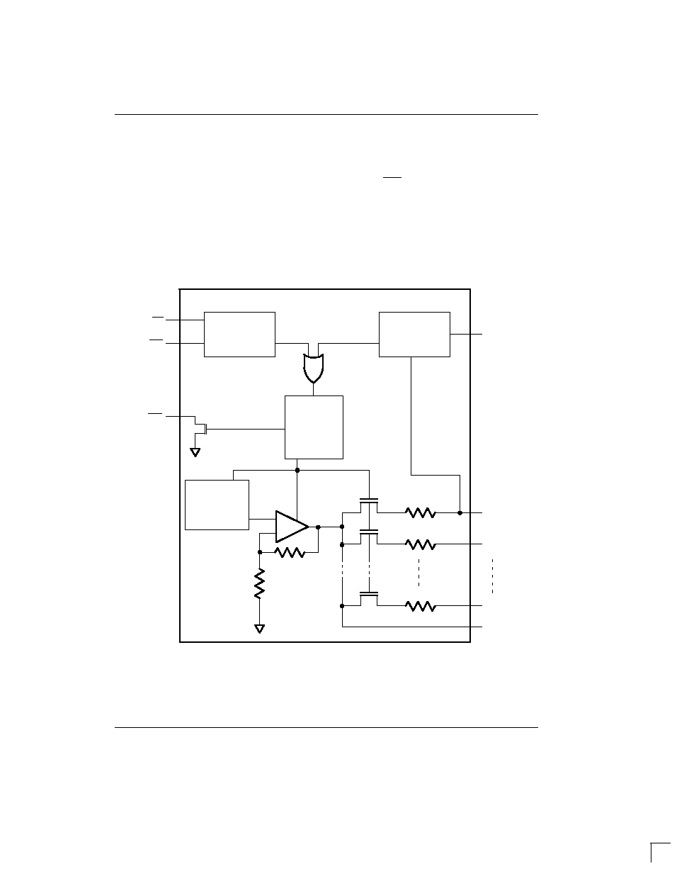
The DS2109 consists of 3 major functional blocks,
Figure 2:
∑
Voltage reference, terminating resistors, and isolation
switches
∑
Bus current sensing circuitry
∑
Bus ground sensing circuity
When the Bus Ground Sensing Circuitry or Bus Current
Sensing Circuitry determine that the SCSI bus is prop-
erly terminated without the DS2109, the power down
buffer isolates the resistors from the SCSI bus and dis-
ables the power amp, thereby placing the DS2109 in a
low power mode (the bus sensing circuitry always stays
active). The PDO (Power Down Output) pin can be con-
nected to the pin of a DS21S07A SCSI terminator for
Wide SCSI configurations, Figure 8.
DS2109 BLOCK DIAGRAM Figure 2
V
REF
+
≠
TCS
R14
R18
R1
110 OHMS
110 OHMS
110 OHMS
BANDGAP
REFERENCE
POWER
DOWN
BUFFER
BUS CURRENT
SENSING
CIRCUITRY
BUS GROUND
SENSING
CIRCUITRY
PDI
PDE
PDO
DISABLE
DISABLE
DS2109
022698 4/10
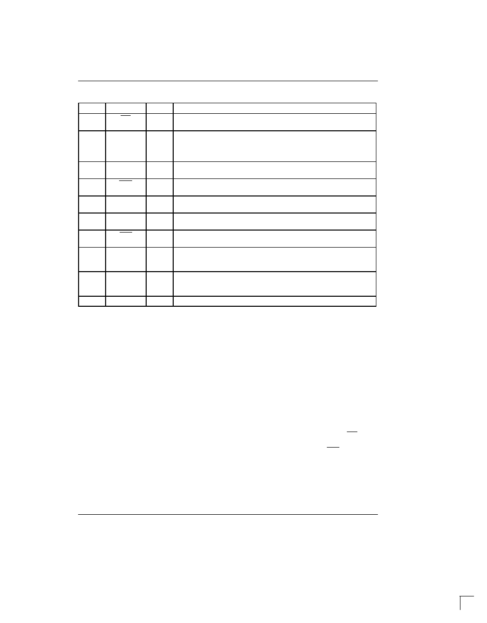
DETAILED PIN DESCRIPTION Table 1
PIN
SYMBOL
FCN
DESCRIPTION
1
PDI
I
Power Down Internal. For Bus Ground Sensing Circuit connect to pin 22
of internal SCSI connector, see Figure 4.
2≠6,
10≠13,
16≠19,
24≠27
R1...R13
R15...18
T
Signal Termination. 110 ohm termination. Connect to SCSI bus signal
lines. For Bus Current Sensing Circuit connect to data, parity, and control
lines, except SCSI≠RST line, see Figure 6.
7, 8, 21
HS≠GND
P
Heat Sink Ground. Internally connected to the mounting pad. Should be
either grounded or electronically isolated from other circuitry.
9
PDO
O
Power Down Output. Connect to DS21S07A for Wide SCSI applica-
tions, see Figure 8.
14
TPWR
P
Termination Power. Connect to the SCSI TERMPWR line. Bypass with
a 2.2
µ
F capacitor, see Figures 4 and 6.
15
V
REF
O
Reference Voltage. 2.85 volt reference; must be decoupled with a 4.7
µ
F
capacitor, see Figures 4 and 6.
20
PDE
I
Power Down External. For Bus Ground Sensing Circuit, connect to pin
36 of external SCSI connector, see Figure 4.
22
TCS
I
Termination Current Sense. Used to sense current on the SCSI bus.
For Bus Current Sensing Circuit, connect to SCSI signal line ≠RST, see
Figure 6.
23
R14
T
Signal Termination. 110 ohm termination. Connect to SCSI bus signal
line. For Bus Current Sensing Circuit connect to SCSI controller chip, see
Figure 6.
28
GND
P
Ground. Signal ground; 0.0 volts.
ACTIVE TERMINATION
The voltage regulator circuitry (bandgap reference and
class AB power amplifier) produces a precise laser≠
trimmed 2.85 volt level and is capable of sourcing 24 mA
into each of the terminating resistors when the signal
line is low (active). When the external driver for a given
signal line turns off, the active terminator will pull that
signal line to 2.85 volts (quiescent state). When used
with an active negation driver, the power amp can sink
22 mA per line while keeping the voltage reference in
regulation; the terminating resistors maintain their 110
value over the entire voltage range. To maintain the spe-
cified regulation, a 4.7
µ
F capacitor is required between
the V
REF
pin and ground. A high frequency cap (0.1
µ
F
ceramic recommended) can also be placed on the V
REF
pin in applications that use fast rise/fall time drivers. The
power down capacitance on terminating resistors
R1≠R13 and R15≠R18 is <4 pF; R14 is slightly higher
due to the bus current sensing circuitry.
The DS2109 can be removed from the SCSI bus by
using either of two automatic methods, Bus Ground
Sensing or Bus Current Sensing.
As with all analog circuitry, the TERMPWR lines should
be bypassed locally. A 2.2
µ
F capacitor is recom-
mended between TPWR and ground and placed as
close as possible to the DS2109. The DS2109 should
be placed as close as possible to the connector to mini-
mize signal and power trace length, thereby resulting in
less input capacitance and reflections which can
degrade the bus signals.
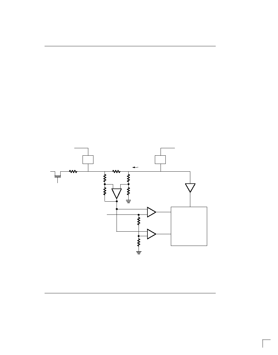
BUS GROUND SENSING
If internal and external SCSI devices are connected to
the SCSI bus, the DS2109 will disconnect from the SCSI
bus according to the circuit in Figure 3. To utilize this
automatic disconnect method of bus sensing, configure
the DS2109 as shown in Figure 4. The PDI (Power
Down Internal) pin should be connected to pin 22 of the
internal SCSI connector, and the PDE (Power Down
External) connected to pin 36 of the external SCSI con-
nector.
DS2109
022698 5/10
BUS GROUND SENSING CIRCUIT Figure 3
PDE
PDI
DISABLE
BUS GROUND DETECT CONFIGURATION Figure 4
V
REF
INTERNAL SCSI CONNECTOR
EXTERNAL
SCSI
CONNECT
OR
22
26
38
36
TERMPWR
2.2
µ
F
4.7
µ
F
DS2109
PDI
TPWR
GND
PDE
DS2109
022698 6/10
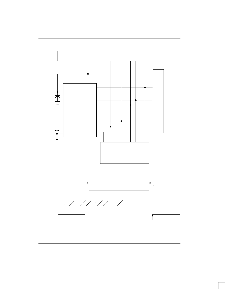
BUS CURRENT SENSING
The DS2109 has the capability to use current sensing to
determine if the SCSI bus is over≠ or under≠terminated.
A series 1 ohm resistor between pads R14 and TCS is
inserted into the SCSI bus (preferably the ≠RST line)
and used to monitor the current when that line pulls low
(active, or "asserted" state). Based on the current mea-
sured, the DS2109 will disconnect or connect from the
SCSI bus. The configuration for this automatic isolation
technique is shown in Figure 6.
Figure 5 shows a simplified diagram of the sensing cir-
cuit. The voltage across the 1 ohm sense resistor is dif-
ferentially amplified and converted into a single≠ended
voltage with respect to ground. This is fed into a bank of
comparators and measured against a reference volt-
age. The circuit takes a measurement each time TCS is
driven below a 0.8 volts threshold and the outputs are
latched on the rising edge of TCS. If I
BUS
is greater than
32 mA, the DS2109 will be isolated from the SCSI bus. It
is recommended that the signal on TCS be asserted for
at least 25 msec to allow the signal (and comparator out-
puts) to settle into a known state. A timing diagram of the
sensing and latching operation is shown in Figure 7.
It is preferred that the ≠RST line be used for monitoring
the bus termination status because ≠RST is only
asserted during power up or during a major change in
bus configuration. Note that R14 will have a higher input
capacitance than the other lines because of the addi-
tional circuitry required for bus sensing.
The DS2109 will be isolated from the SCSI bus as
shown in Table 2.
BUS CURRENT SENSING CIRCUITRY Figure 5
REF
DECODE
AND
LATCH
TCS
R14
1 OHM
110 OHM
+
≠
I
BUS
TO SCSI CONTROLLER
FROM SCSI BUS (≠RST)
DS2109
022698 7/10
BUS CURRENT SENSE CONFIGURATION Figure 6
V
REF
INTERNAL SCSI
CONNECTOR
26
40
38
45
≠RST
≠RST
SCSI
CONTROLLER
EXTERNAL
SCSI
CONTROLLER
TERMPWR
DS2109
TPWR
GND
R1
R13
R15
R18
TCS
R14
2.2
µ
F
4.7
µ
F
BUS CURRENT SENSE TIMING DIAGRAM Figure 7
25
µ
s min
TCS
COMPARATORS
LATCH

DS2109
022698 8/10
DISCONNECT MODES Table 2
PDI
PDE
I
BUS
> 32 mA?
DS2109 ISOLATED
FROM SCSI BUS?
0
0
No
Isolated
0
1
No
Connected
1
0
No
Connected
1
1
No
Connected
0
0
Yes
Isolated
0
1
Yes
Isolated
1
0
Yes
Isolated
1
1
Yes
Isolated
NOTE: "1" denotes pin left open circuited.
WIDE SCSI CONFIGURATION Figure 8
PD
V
REF2
NC
R9
R8
R7
R6
TERMPWR2
4.7
µ
F
GND
R18
R17
R16
R15
R14
TCS
HS≠GND
PDE
R13
R12
R11
R10
V
REF
1
2
3
4
5
6
7
8
9
10
11
12
13
14
28
27
26
25
24
23
22
21
20
19
18
17
16
15
PDI
R1
R2
R3
R4
R5
HS≠GND
HS≠GND
PDO
R6
R7
R8
R9
TPWR
1
2
3
4
5
6
7
8
16
15
14
13
12
11
10
9
TERMPWR1
R1
R2
R3
R4
R5
V
REF1
GND
DS21S07A 16≠PIN SOIC (300 MIL)
2.2
µ
F
TERMINATION POWER LINE
DS2109S 28≠PIN SOIC (300 MIL)
4.7
µ
F

DS2109
022698 9/10
ABSOLUTE MAXIMUM RATINGS*
Voltage on Any Pin Relative to Ground
≠1.0V to +7.0V
Operating Temperature
0
∞
C to 70
∞
C
Storage Temperature
≠55
∞
C to +125
∞
C
Soldering Temperature
260
∞
C for 10 seconds
* This is a stress rating only and functional operation of the device at these or any other conditions above those
indicated in the operation sections of this specification is not implied. Exposure to absolute maximum rating
conditions for extended periods of time may affect reliability.
RECOMMENDED OPERATING CONDITIONS
(0
∞
C to 70
∞
C)
PARAMETER
SYMBOL
MIN
TYP
MAX
UNITS
NOTES
TERMPWR Voltage
V
TP
4.00
5.25
V
Logic 1
V
IH
2.0
V
TP
+0.3
V
1
Logic 0
V
IL
≠0.3
+0.8
V
1
DC CHARACTERISTICS
(0
∞
C to 70
∞
C)
PARAMETER
SYMBOL
MIN
TYP
MAX
UNITS
NOTES
TERMPWR Current
I
TP
I
TP
10
500
14
mA
mA
2, 4
2, 5
Power Down Current
I
PD
1
2
mA
2, 3, 6
Termination Resistance
R
TERM
108
110
112
ohms
2, 3
Die Thermal Shutdown
TS
D
150
∞
C
2
Power Down Termination
Capacitance
C
PD
C
14
3
8
4.5
pF
pF
2, 3, 6, 7
2,3,6,7,8
Input Leakage High
I
IH
≠1.0
µ
A
2, 12
Input Leakage Low
I
IL
1.0
µ
A
2, 9, 12
Output Current
I
O
4
mA
10
Bus Current Sense Trip Point
I
BCST
32
mA
11
REGULATOR CHARACTERISTICS
(0
∞
C to 70
∞
C)
PARAMETER
SYMBOL
MIN
TYP
MAX
UNITS
NOTES
Output Voltage
V
REF
2.79
2.85
2.91
V
2, 3
Drop Out Voltage
V
DROP
0.75
1.0
V
4, 7
Line Regulation
LI
REG
1.0
2.0
%
2, 5
Load Regulation
LO
REG
1.3
3.0
%
2, 3
Current Limit
I
L
700
mA
2
Sink Current
I
SINK
400
mA
2
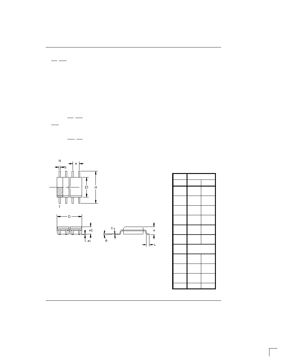
The chamfer on the body is optional. If it is not present, a termi-
nal 1 identifier must be positioned so that 1/2 or more of its area
is contained in the hatched zone.
DS2109
022698 10/10
NOTES:
1. PDI, PDE, TCS
2. 4.00V < TERMPWR < 5.25V.
3. 0.0V < signal lines < 3.0V.
4. All signal lines = 0.0V.
5. All signal lines open.
6. Power down enabled.
7. Guaranteed by design; not production tested.
8. C
14
slightly higher capacitance due to sensing circuitry.
9. Excluding PDI, PDE pins.
10. PDO output pin.
11. I
BCST
> 32 mA ≠ disable termination.
12. Excluding PDE, PDI, R14, and TCS pins.
28≠PIN SOIC (300 MIL)
PKG
28≠PIN
DIM
MIN
MAX
A IN.
MM
0.094
2.39
0.105
2.67
A1 IN.
MM
0.004
0.102
0.012
0.30
A2 IN.
MM
0.089
2.26
0.095
2.41
b IN.
MM
0.013
0.33
0.020
0.51
C IN
MM
0.009
0.229
0.013
0.33
D IN.
MM
0.698
17.73
0.712
18.08
e IN.
MM
0.050 BSC
1.27 BSC
E1 IN.
MM
0.290
7.37
0.300
7.62
H IN
MM
0.398
10.11
0.416
10.57
L IN
MM
0.016
0.40
0.040
1.02
0
∞
8
∞