 | ÐлекÑÑоннÑй компоненÑ: DS1602 | СкаÑаÑÑ:  PDF PDF  ZIP ZIP |
Äîêóìåíòàöèÿ è îïèñàíèÿ www.docs.chipfind.ru
1 of 10
070199
FEATURES
§
Two 32bit counters keep track of real time
and elapsed time
§
Counters keep track of seconds for over 125
years
§
Battery powered counter counts seconds from
the time battery is attached until V
BAT
is less
than 2.5 volts
§
V
CC
powered counter counts seconds while
V
CC
is above 4.25 volts and retains the count
in the absence of V
CC
under battery backup
power
§
Clear function resets selected counter to 0
§
Read/Write serial port affords low pin count
§
Maximum current drain of less than 1 µA
from V
BAT
pin when serial port is disabled
§
One byte protocol defines read/write, counter
address and software clear function
§
8pin DIP or optional 8pin SOIC
§
Operating temperature range of 40°C to
+85°C
§
Reduced performance operation down to V
CC
= 2.5V
PIN ASSIGNMENT
PIN DESCRIPTION
RST
- Reset
CLK
- Clock
DQ
- Data Input/Output
GND
- Ground
X1, X2
- Crystal Inputs
V
BAT
- + Battery Input
V
CC
- +5 Volts
DESCRIPTION
The DS1602 is a real time clock/elapsed time counter designed to count seconds when V
CC
power is
applied and continually count seconds under battery backup power with an additional counter regardless
of the condition of V
CC
. The continuous counter can be used to derive time of day, week, month, and year
by using a software algorithm. The V
CC
powered counter will automatically record the amount of time
that V
CC
power is applied. This function is particularly useful in determining the operational time of
equipment in which the DS1602 is used. Alternatively, this counter can also be used under software
control to record real time events. Communication to and from the DS1602 takes place via a 3wire
serial port. A 1-byte protocol selects read/ write functions, counter clear functions and oscillator trim. A
low cost 32.768 kHz crystal attaches directly to the X1 and X2 pins. If battery powered-only operation is
desired, the V
BAT
pin must be grounded and the V
CC
pin must be connected to the battery.
DS1602
8-Pin SOIC (200-mil)
DS1602
8-Pin DIP (300-mil)
DS1602
Elapsed Time Counter
www.dalsemi.com
V
CC
V
BAT
X1
X2
RST
DQ
CLK
GND
1
2
3
4
8
7
6
5
RST
DQ
CLK
GND
V
CC
V
BAT
X1
X2
1
2
3
4
8
7
6
5

DS1602
2 of 10
OPERATION
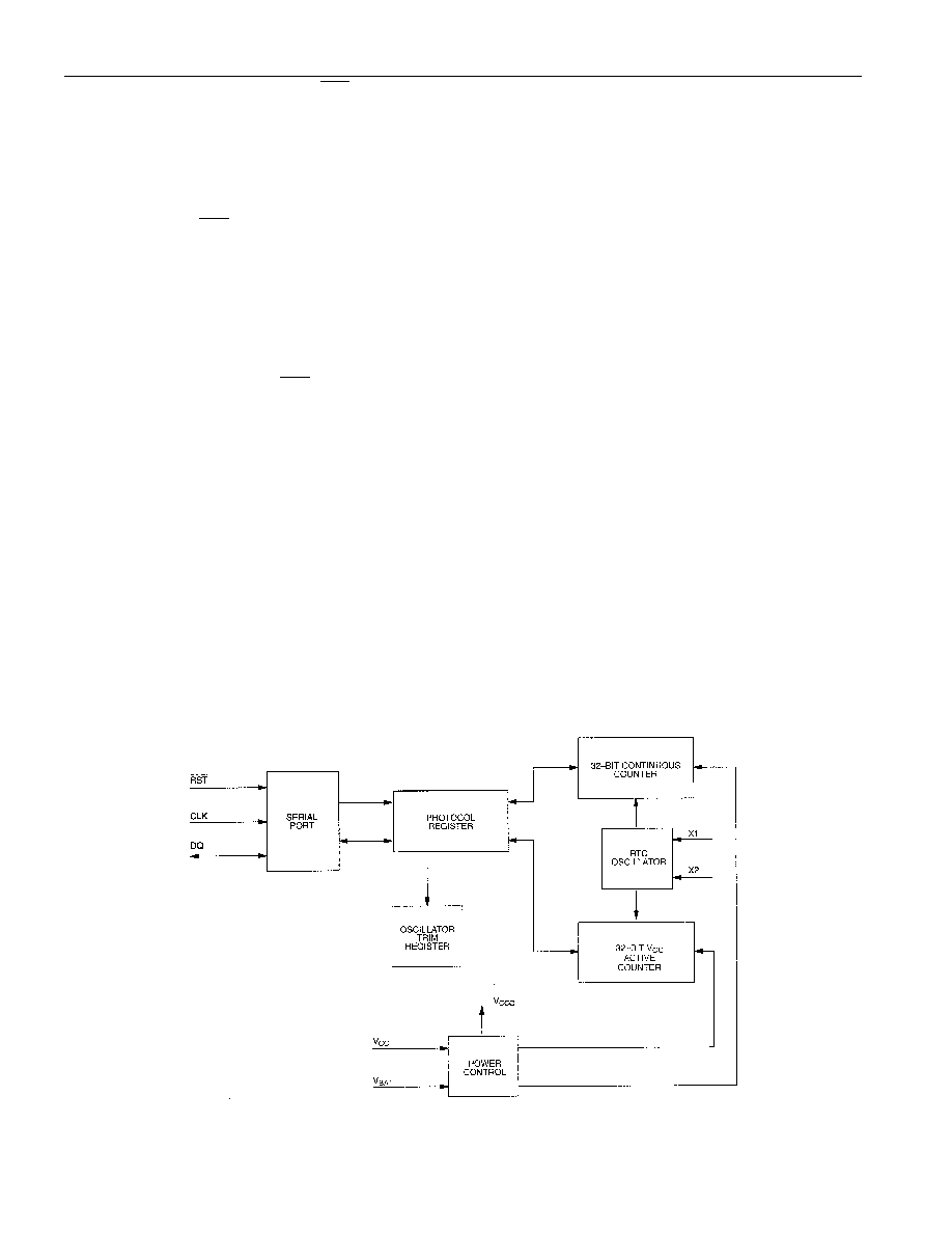
The main elements of the DS1602 are shown in Figure 1. As shown, communications to and from the
elapsed time counter occur over a 3wire serial port. The port is activated by driving
RST
to a high state.
With
RST
at high level, 8 bits are loaded into the protocol shift register providing read/write, register
select, register clear, and oscillator trim information. Each bit is serially input on the rising edge of the
clock input. After the first eight clock cycles have loaded the protocol register with a valid protocol,
additional clocks will output data for a read or input data for a write. V
CC
must be present to access the
DS1602. If V
CC
< V
BAT,
the DS1602 will go into a battery backup mode which disables the serial port to
conserve battery capacity. For battery only operations, the V
BAT
pin must be grounded and the V
CC
pin
must be connected to the battery. This will keep the DS1602 out of battery backup mode. Battery
powered operation down to 2.5V is possible with reduced speed performance on the serial port.
PROTOCOL REGISTER
The protocol bit definition is shown in Figure 2. Valid protocols and the resulting actions are shown in
Table 1. Each data transfer to the protocol register designates what action is to occur. As defined, the
MSB (bit 7 which is designated ACC) selects the 32bit continuous counter for access. If ACC is a
logical 1 the continuous counter is selected and the 32 clock cycles that follow the protocol will either
read or write this counter. If the counter is being read, the contents will be latched into a different register
at the end of protocol and the latched contents will be read out on the next 32 clock cycles. This avoids
reading garbled data if the counter is clocked by the oscillator during a read. Similarly, if the counter is to
be written, the data is buffered in a register and all 32 bits are jammed into the counter simultaneously on
the rising edge of the 32
nd
clock. The next bit (bit 6 which is designated AVC) selects the 32bit V
CC
active counter for access. If AVC is a logical 1 this counter is selected and the 32 clock cycles that follow
will either read or write this counter. If both bit 7 and bit 6 are written to a logic high, all clock cycles
beyond the protocol are ignored and bits 5, 4, and 3 are loaded into the oscillator trim register. A value of
binary 3 (011) will give a clock accuracy of ±120 seconds per month at 25
°
C. Increasing the binary
number towards 7 will cause the real time clock to run faster. Conversely, lowering the binary number
towards 0 will cause the clock to run slower. Binary 000 will stop the oscillator completely. This feature
can be used to conserve battery life during storage. In this mode the I
BAT
current is reduced to 100 nA
maximum. In applications where oscillator trimming is not practical or not needed, a default setting of
011 is recommended. Bit 2 of protocol (designated CCC) is used to clear the continuous counter. When
set to logic 1, the continuous counter will reset to 0 when
RST
is taken low. Bit 1 of protocol (designated
CVC) is used to clear the V
CC
active counter. When set to logical 1, the V
CC
active counter will reset to 0
when
RST
is taken low. Both counters can be reset simultaneously by setting CCC and CVC both to a
logical 1. Bit 0 of the protocol (designated RD) determines whether the 32 clocks to follow will write a
counter or read a counter. When RD is set to a logical 0 a write action will follow when RD is set to a
logical 1 a read action will follow. When sending the protocol, 8 bits should always be sent. Sending less
than 8 bits can produce erroneous results. If clearing the counters or trimming the oscillator, the data
transfer can be terminated after the 8bit protocol is sent. However, when reading or writing the counters,
32 clock cycles should always follow the protocol.
RESET AND CLOCK CONTROL
All data transfers are initiated by driving the
RST
input high. The
RST
input has two functions. First,
RST
turns on the serial port logic which allows access to the protocol register for the protocol data entry.
Second, the
RST
signal provides a method of terminating the protocol transfer or the 32bit counter
transfer. A clock cycle is a sequence of a falling edge followed by a rising edge. For write inputs, data
must be valid during the rising edge of the clock. Data bits are output on the falling edge of the clock
when data is being read. All data transfers terminate if the
RST
input is transitioned low and the DQ pin
DS1602
3 of 10
goes to a high impedance state.
RST
should only be transitioned low while the clock is high to avoid
disturbing the last bit of data. All data transfers must consist of 8 bits when transferring protocol only or 8
+ 32 bits when reading or writing either counter. Data transfer is illustrated in Figure 3.
DATA INPUT
Following the 8bit protocol that inputs write mode, 32 bits of data are written to the selected counter on
the rising edge of the next 32 CLK cycles. After 32 bits have been entered any additional CLK cycles will
be ignored until
RST
is transitioned low to end data transfer, and then high again to begin new data
transfer.
DATA OUTPUT
Following the eight CLK cycles that input read mode protocol, 32 bits of data will be output from the
selected counter on the next 32 CLK cycles. The first data bit to be transmitted from the selected 32bit
counter occurs on the falling edge after the last bit of protocol is written. When transmitting data from
the selected 32bit counter,
RST
must remain at high level as a transition to low level will terminate data
transfer. Data is driven out the DQ pin as long as CLK is low. When CLK is high the DQ pin is tristated.
CRYSTAL SELECTION
A standard 32.768 kHz quartz crystal can be directly connected to the DS1602 via pins 1 and 2 (X1, X2).
The crystal selected for use should have a specified load capacitance (C
L
) of 6 pF. For more information
on crystal selection and crystal layout considerations, please consult Application Note 58, "Crystal
Considerations with Dallas Real Time Clocks."
BATTERY SELECTION
The battery selected for use with the DS1602 should have an output voltage between 2.5 and 3.5 volts. A
lithium battery of 35 mAh or greater will run the elapsed time counter for over 10 years in the absence of
power. Small lithium coin cell batteries produce both the proper output voltage and have the capacity to
supply the DS1602 for the useable lifetime of the equipment where they are installed.
DS1602 ELAPSED TIME COUNTER BLOCK DIAGRAM Figure 1

DS1602
4 of 10
PROTOCOL BIT MAP Figure 2
7
6
5
4
3
2
1
0
ACC
AVC
OSC2
OSC1
OSC0
CCC
CVC
RD

DS1602
5 of 10
VALID PROTOCOLS Table 1
PROTOCOL
ACTION
ACC
AVC
OSC2
OSC1 OSC0
CCC CVC RD DESCRIPTION
Read
Continuous
Counter
1
0
X
X
X
X
X
1
Output continuous
counter on the 32 clocks
following protocol.
Oscillator trim register
is not updated.
Counters are not reset.
Write
Continuous
Counter
1
0
X
X
X
X
X
0
Input data to continuous
counter on the 32 clocks
following protocol.
Oscillator trim register
is not updated.
Counters are not reset.
Read V
CC
Active
Counter
0
1
X
X
X
X
X
1
Output V
CC
active
counter on the 32 clocks
following protocol,
oscillator trim register
is not updated.
Counters are not reset.
Write V
CC
Active
Counter
0
1
X
X
X
X
X
0
Input data to continuous
counter on the 32 clocks
following protocol.
Oscillator trim register
is not updated.
Counters are not reset.
Clear
Continuous
Counter
0
0
X
X
X
1
X
X
Resets the continuous
counter to all zeroes at
the end of protocol.
Oscillator trim register
is not updated.
Clear V
CC
Active
Counter
0
0
X
X
X
X
1
X
Resets the V
CC
active
counter to all zeroes at
the end of protocol.
Oscillator trim register
is not updated.
Set Oscillator
Trim Bits
1
1
A
B
C
X
X
0
Sets the oscillator trim
register to a value of
ABC. Counters are
unaffected.
X = Don't Care