 | –≠–ª–µ–∫—Ç—Ä–æ–Ω–Ω—ã–π –∫–æ–º–ø–æ–Ω–µ–Ω—Ç: DS1486P | –°–∫–∞—á–∞—Ç—å:  PDF PDF  ZIP ZIP |

1 of 17
072401
FEATURES
ß 128 kbytes of user NV RAM
ß Integrated NV SRAM, real-time clock,
crystal, power-fail control circuit and lithium
energy source
ß Totally nonvolatile with over 10 years of
operation in the absence of power
ß Watchdog timer restarts an out-of-control
processor
ß Alarm function schedules real-time related
activities such as system wakeup
ß Programmable interrupts and square wave
output
ß All registers are individually addressable via
the address and data bus
ß Interrupt signals active in power-down mode
ORDERING INFORMATION
DS1486
XXX
(32≠pin DIP module)
≠150
150 ns access
≠120
120 ns access
*DS1486P
XXX
34-pin PowerCap Module Board
≠150
150 ns access
≠120
120 ns access
*DS9034PCX PowerCap Required
(must be ordered separately)
PIN DESCRIPTION
INTB
≠ Interrupt Output A (open drain)
INTB
(INTB) ≠ Interrupt Output B (open drain)
A0≠A16 ≠
Address
Inputs
DQ0≠DQ7 ≠
Data
Input/Output
CE
≠ Chip Enable
OE
≠ Output Enable
WE
≠ Write Enable
V
CC
≠ +5 Volts
GND ≠
Ground
SQW
≠ Square Wave Output
NC
≠ No Connection
X1, X2
≠ Crystal Connection
V
BAT
≠ Battery Connection
PIN ASSIGNMENT
DS1486/DS1486P
RAMified Watchdog Timekeeper
www.maxim-ic.com
34
1
INTB (INTB)
2
3
A15
A16
PFO
V
CC
WE
OE
CE
DQ7
DQ6
DQ5
DQ4
DQ3
DQ2
DQ1
DQ0
GND
4
5
6
7
8
9
10
11
12
13
14
15
16
17
SQW
A14
33
32
31
30
29
28
27
26
25
24
23
22
21
20
19
18
A13
A12
A11
A10
A9
A8
A7
A6
A5
A4
A3
A2
A1
A0
INTA
X1 GND V
BAT
X2
34-Pin PowerCap Module Board
(Uses DS9034PCX PowerCap)
INTB (INTB)
13
1
2
3
4
5
6
7
8
9
10
11
12
14
31
DS1486 128k x 8
32-Pin Encapsulated Package
A14
A7
A5
A4
A3
A2
A1
A0
DQ1
DQ0
V
CC
A15
INTA/SQW
WE
A13
A8
A9
A11
OE
A10
CE
DQ7
DQ5
DQ6
32
30
29
28
27
26
25
24
23
22
21
19
20
A16
A12
A6
DQ2
GND
15
16
18
17
DQ4
DQ3

DS1486/DS1486P
2 of 17
DESCRIPTION
The DS1486 is a nonvolatile Static RAM with a full function Real-time clock (RTC), alarm, watchdog
timer, and interval timer which are all accessible in a bytewide format. The DS1486 contains a lithium
energy source and a quartz crystal which eliminate the need for any external circuitry. Data contained
within 128K by 8-bit memory and the timekeeping registers can be read or written in the same manner as
bytewide static RAM. The timekeeping registers are located in the first 14 bytes of memory space. Data
is maintained in the RAMified Timekeeper by intelligent control circuitry which detects the status of V
CC
and write-protects memory when V
CC
is out of tolerance. The lithium energy source can maintain data and
real time for over 10 years in the absence of V
CC
. Timekeeper information includes hundredths of
seconds, seconds, minutes, hours, day, date, month, and year. The date at the end of the month is
automatically adjusted for months with less than 31 days, including correction for leap year. The
RAMified Timekeeper operates in either 24-hour or 12-hour format with an AM/PM indicator. The
watchdog timer provides alarm interrupts and interval timing between 0.01 seconds and 99.99 seconds.
The real time alarm provides for preset times of up to one week. Interrupts for both watchdog and RTC
will operate when system is powered down. Either can provide system "wake-up" signals.
PACKAGES
The DS1486 is available in two packages: 32-pin DIP module and 34-pin PowerCap module. The 32-pin
DIP style module integrates the crystal, lithium energy source, and silicon all in one package. The 32-pin
PowerCap Module Board is designed with contacts for connection to a separate PowerCap
(DS90934PCX) that contains the crystal and battery. The design allows the PowerCap to be mounted on
top of the DS1486P after the completion of the surface mount process. Mounting the PowerCap after the
surface mount process prevents damage to the crystal and battery due to high temperatures required for
solder reflow. The PowerCap is keyed to prevent reverse insertion. The PowerCap Module Board and
PowerCap are ordered separately and shipped in separate containers. The part number for the PowerCap
is DS9034PCX.
OPERATION - READ REGISTERS
The DS1486 executes a read cycle whenever
WE
(Write Enable) is inactive (High),
CE
(Chip Enable)
and
OE
(Output Enable) are active (Low). The unique address specified by the address inputs (A0-A16)
defines which of the registers is to be accessed. Valid data will be available to the eight data output
drivers within t
ACC
(Access Time) after the last address input signal is stable, providing that
CE
and
OE
access times are also satisfied. If
OE
and
CE
access times are not satisfied, then data access must be
measured from the latter occurring signal (
CE
or
OE
) and the limiting parameter is either t
CO
for
CE
or
t
OE
for
OE
rather than address access.
OPERATION - WRITE REGISTERS
The DS1486 is in the write mode whenever the
WE
(Write Enable) and
CE
(Chip Enable) signals are in
the active (Low) state after the address inputs are stable. The latter occurring falling edge of
CE
or
WE
will determine the start of the write cycle. The write cycle is terminated by the earlier rising edge of
CE
or
WE
. All address inputs must be kept valid throughout the write cycle.
WE
must return to the high state
for a minimum recovery state (t
WR
) before another cycle can be initiated. Data must be valid on the data
bus with sufficient Data Set-Up (t
DS
) and Data Hold Time (t
DH
) with respect to the earlier rising edge of
CE
or
WE
. The
OE
control signal should be kept inactive (High) during write cycles to avoid bus
contention. However, if the output bus has been enabled (
CE
and
OE
active), then
WE
will disable the
outputs in t
ODW
from its falling edge.

DS1486/DS1486P
3 of 17
DATA RETENTION
The RAMified Timekeeper provides full functional capability when V
CC
is greater than 4.5 volts and
write-protects the register contents at 4.25 volts typical. Data is maintained in the absence of V
CC
without
any additional support circuitry. The DS1486 constantly monitors V
CC
. Should the supply voltage decay,
the RAMified Timekeeper will automatically write-protect itself and all inputs to the registers become
"don't care." The two interrupts
INTA
and
INTB
(INTB) and the internal clock and timers continue to run
regardless of the level of V
CC
. However, it is important to insure that the pull-up resistors used with the
interrupt pins are never pulled up to a value that is greater than V
CC
+ 0.3V. As V
CC
falls below
approximately 3.0 volts, a power switching circuit turns the internal lithium energy source on to maintain
the clock and timer data functionality. It is also required to insure that during this time (battery backup
mode), the voltage present at
INTA
and
INTB
(INTB) never exceeds V
BAT
. During power-up, when V
CC
rises above approximately 3.0 volts, the power switching circuit connects external V
CC
and disconnects
the internal lithium energy source. Normal operation can resume after V
CC
exceeds 4.5 volts for a period
of 200 ms.
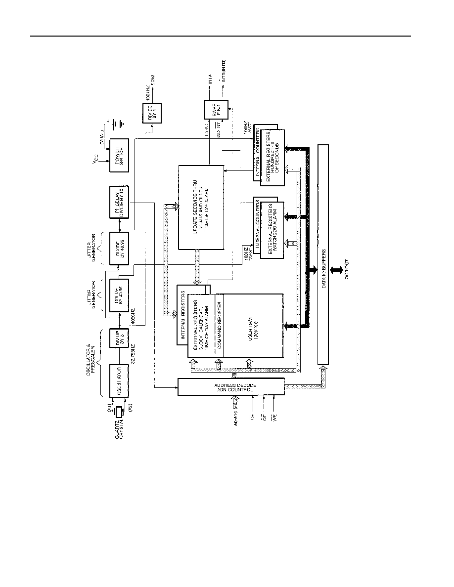
RAMIFIED TIMEKEEPER REGISTERS
The RAMified Timekeeper has 14 registers which are 8 bits wide that contain all of the timekeeping,
alarm, watchdog and control information. The clock, calendar, alarm, and watchdog registers are memory
locations which contain external (user-accessible) and internal copies of the data. The external copies are
independent of internal functions except that they are updated periodically by the simultaneous transfer of
the incremented internal copy (see Figure 1). The Command Register bits are affected by both internal
and external functions. This register will be discussed later. Registers 0, 1, 2, 4, 6, 8, 9, and A contain
time of day and date information (see Figure 2). Time of day information is stored in BCD. Registers 3,
5, and 7 contain the Time of Day Alarm information. Time of Day Alarm information is stored in BCD.
Register B is the Command Register and information in this register is binary. Registers C and D are the
Watchdog Alarm Registers and information which is stored in these two registers is in BCD. Registers E
through 1FFFF are user bytes and can be used to maintain data at the user's discretion.
CLOCK ACCURACY (DIP MODULE)
The DS1486 is guaranteed to keep time accuracy to within
±1 minute per month at 25∞C.
CLOCK ACCURACY (POWERCAP MODULE)
The DS1486P and DS9034PCX are each individually tested for accuracy. Once mounted together, the
module is guaranteed to keep time accuracy to within ±1.53 minutes per month (35 ppm) at 25∞C.
DS1486/DS1486P
4 of 17
BLOCK DIAGRAM Figure 1

DS1486/DS1486P
5 of 17
TIME OF DAY REGISTERS
Registers 0, 1, 2, 4, 6, 8, 9, and A contain Time of Day data in BCD. Ten bits within these eight registers
are not used and will always read 0 regardless of how they are written. Bits 6 and 7 in the Months
Register (9) are binary bits. When set to logic 0,
EOSC
(Bit 7) enables the real-time clock oscillator. This
bit is set to logic 1 as shipped from Dallas Semiconductor to prevent lithium energy consumption during
storage and shipment (DIP Module only). This bit will normally be turned on by the user during device
initialization. However, the oscillator can be turned on and off as necessary by setting this bit to the
appropriate level. The
INTA
and Square Wave Output signals are tied together at pin 30 on the 32-pin
DIP module. With this package, bit 6 of the Months Register (9) controls the function of this pin. When
set to logic 0, the pin will output a 1024 Hz square wave signal. When set to logic 1, the pin is available
for interrupt A output (
INTA
) only. The
INTA
and Square Wave Output signals are separated on the 34-
pin PowerCap module. With this package, bit 6 of the Months Register (9) controls only the Square Wave
Output (pin 33). When set to logic 0, pin 33 will output a 1024 Hz square wave signal. When set to logic
1, pin 33 is in a high impedance state. Pin 34 (
INTA
) is not affected by the setting of bit 6. Bit 6 of the
Hours register is defined as the 12- or 24-hour select bit. When set to logic 1, the 12-hour format is
selected. In the 12-hour format, bit 5 is the AM/PM bit with logic 1 being PM. In the 24-hour mode, bit 5
is the second 10-hour bit (20-23 hours). The Time of Day registers are updated every 0.01 seconds from
the real-time clock, except when the TE bit (bit 7 of Register B) is set low or the clock oscillator is not
running. The preferred method of synchronizing data access to and from the RAMified Timekeeper is to
access the Command register by doing a write cycle to address location 0B and setting the TE bit
(Transfer Enable bit) to a logic 0. This will freeze the External Time of Day registers at the present
recorded time, allowing access to occur without danger of simultaneous update. When the watch registers
have been read or written, a second write cycle to location 0B setting the TE bit to a logic 1 will put the
Time of Day Registers back to being updated every 0.01 second. No time is lost in the real-time clock
because the internal copy of the Time of Day register buffers is continually incremented while the
external memory registers are frozen. An alternate method of reading and writing the Time of Day
registers is to ignore synchronization. However, any single reading may give erroneous data as the real-
time clock may be in the process of updating the external memory registers as data is being read. The
internal copies of seconds through years are incremented and the Time of Day Alarm is checked during
the period that hundreds of seconds reads 99. The copies are transferred to the external register when
hundredths of seconds roll from 99 to 00. A way of making sure data is valid is to do multiple reads and
compare. Writing the registers can also produce erroneous results for the same reasons. A way of making
sure that the write cycle has caused proper a update is to do read verifies and re-execute the write cycle if
data is not correct. While the possibility of erroneous results from read and write cycles has been stated, it
is worth noting that the probability of an incorrect result is kept to a minimum due to the redundant
structure of the RAMified Timekeeper.
TIME OF DAY ALARM REGISTERS
Registers 3, 5, and 7 contain the Time of Day Alarm Registers. Bits 3, 4, 5, and 6 of Register 7 will
always read 0 regardless of how they are written. Bit 7 of Registers 3, 5, and 7 are mask bits (Figure 3).
When all of the mask bits are logic 0, a Time of Day Alarm will only occur when Registers 2, 4, and 6
match the values stored in Registers 3, 5, and 7. An alarm will be generated every day when bit 7 of
Register 7 is set to a logic 1. Similarly, an alarm is generated every hour when bit 7 of Registers 7 and 5
is set to a logic 1. When bit 7 of Registers 7, 5, and 3 is set to a logic 1, an alarm will occur every minute
when Register 1 (seconds) rolls from 59 to 00.
Time of Day Alarm Registers are written and read in the same format as the Time of Day Registers. The
Time of Day Alarm Flag and Interrupt are always cleared when Alarm Registers are read or written.