
1 of 13
REV: 012003
Note: Some revisions of this device may incorporate deviations from published specifications known as errata. Multiple revisions of any device
may be simultaneously available through various sales channels. For information about device errata, click here:
www.maxim-ic.com/errata
.
GENERAL DESCRIPTION
The DS1337 serial real-time clock is a low-power
clock/calendar with two programmable time-of-day
alarms and a programmable square-wave output.
Address and data are transferred serially via a 2-wire,
bidirectional bus. The clock/calendar provides
seconds, minutes, hours, day, date, month, and year
information. The date at the end of the month is
automatically adjusted for months with fewer than 31
days, including corrections for leap year. The clock
operates in either the 24-hour or 12-hour format with
AM/PM indicator.
APPLICATIONS
Handhelds (GPS, POS Terminal, MP3 Player)
Consumer Electronics (Set-Top Box, VCR/Digital
Recording)
Office Equipment (Fax/Printer, Copier)
Medical (Glucometer, Medicine Dispenser)
Telecommunications (Router, Switcher, Server)
Other (Utility Meter, Vending Machine, Thermostat,
Modem)
FEATURES
� Real-Time Clock (RTC) Counts Seconds,
Minutes, Hours, Day, Date, Month, and Year
with Leap-Year Compensation Valid Up to 2100
� Two-Wire Serial Interface
� Two Time-of-Day Alarms
� Oscillator Stop Flag
� Programmable Square-Wave Output
� Defaults to 32kHz on Power-Up
�
Available in 8-Pin DIP, SO, or
mSOP
ORDERING INFORMATION
PART TEMP
RANGE
PIN-PACKAGE
TOP
MARK
DS1337
-40�C to +85�C
8 DIP (300mil)
DS1337
DS1337S
-40�C to +85�C
8 SO (150mil)
DS1337
DS1337U
-40�C to +85�C
8
mSOP
1337
PIN CONFIGURATIONS
DS1337
Serial Real-Time Clock
www.maxim-ic.com
www.maxim-ic.com
TYPICAL OPERATING CIRCUIT
DIP
X1
X2
GND
VCC
SCL
SDA
SQW/INTB
INTA
SO,
mSOP
X1
X2
GND
VCC
SCL
SDA
SQW/INTB
INTA
TOP VIEW
DS1337
DS1337
DS1337
2 of 13
ABSOLUTE MAXIMUM RATINGS
Voltage Range on Any Pin Relative to Ground
-0.3V to +6.0V
Operating Temperature Range
-40�C to +85�C
Storage Temperature Range
-55�C to +125�C
Soldering Temperature Range
See IPC/JEDEC J-STD-020A Specification
Stresses beyond those listed under "Absolute Maximum Ratings" may cause permanent damage to the device. These are stress ratings only,
and functional operation of the device at these or any other conditions beyond those indicated in the operational sections of the specifications is
not implied. Exposure to the absolute maximum rating conditions for extended periods may affect device.
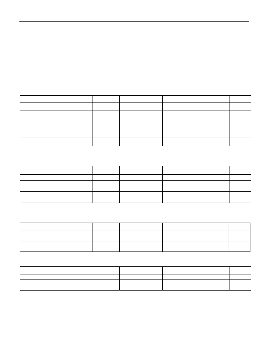
RECOMMENDED DC OPERATING CONDITIONS
(T
A
= -40�C to +85�C)
PARAMETER SYMBOL
CONDITIONS
MIN
TYP
MAX
UNITS
Supply Voltage
V
CC
1.8
4.0
V
Oscillator Voltage
V
OSC
1.3
4.0
V
SCL, SDA
0.7 V
CC
V
CC
+ 0.3
Logic 1
V
IH
INTA, SQW/INTB
5.5
V
Logic 0
V
IL
-0.3
0.3
V
CC
V
DC ELECTRICAL CHARACTERISTICS
(V
CC
= 1.8V to 4.0V, T
A
= -40�C to +85�C.)
PARAMETER SYMBOL
CONDITIONS
MIN
TYP
MAX
UNITS
Input Leakage
I
LI
(Note 1)
1
mA
I/O Leakage
I
LO
(Note 2)
1
mA
Logic 0 Output (V
OL
= 0.4V)
I
OL
(Note
2)
3 mA
Active Supply Current
I
CCA
(Note 3)
150
mA
Standby Current
I
CCS
(Notes 4, 5)
2
mA
DC ELECTRICAL CHARACTERISTICS
(V
CC
= 1.3V to 1.8V, T
A
= -40�C to +85�C.)
PARAMETER SYMBOL
CONDITIONS
MIN
TYP
MAX
UNITS
Timekeeping Current
(Oscillator Enabled)
I
OSC
(Notes 4, 6, 7)
600
nA
Data Retention Current
(Oscillator Disabled)
I
DDR
(Note
4)
50
nA
CRYSTAL SPECIFICATIONS*
PARAMETER SYMBOL
MIN
TYP
MAX
UNITS
Nominal Frequency
F
O
32.768
kHz
Series Resistance
ESR
45
k
Load Capacitance
C
L
6
pF
*The crystal, traces, and crystal input pins should be isolated from RF generating signals. Refer to Application Note 58: Crystal Considerations
for Dallas Real-Time Clocks for additional specifications.

DS1337
3 of 13
AC ELECTRICAL CHARACTERISTICS
(V
CC
= 1.8V to 4.0V, T
A
= -40�C to +85�C.)
PARAMETER SYMBOL
CONDITIONS
MIN TYP
MAX
UNITS
Fast mode
100
400
SCL Clock Frequency
f
SCL
Standard mode
100
kHz
Fast mode
1.3
Bus Free Time Between a
STOP and START Condition
t
BUF
Standard mode
4.7
ms
Fast mode
0.6
Hold Time (Repeated)
START Condition (Note 8)
t
HD:STA
Standard mode
4.0
ms
Fast mode
1.3
LOW Period of SCL Clock
t
LOW
Standard mode
4.7
ms
Fast mode
0.6
HIGH Period of SCL Clock
t
HIGH
Standard mode
4.0
ms
Fast mode
0.6
Setup Time for a Repeated
START Condition
t
SU:STA
Standard mode
4.7
ms
Fast mode
0
0.9
Data Hold Time (Notes 9, 10)
t
HD:DAT
Standard mode
0
ms
Fast mode
100
Data Setup Time (Note 11)
t
SU:DAT
Standard mode
250
ns
Fast mode
20 + 0.1C
B
300
Rise Time of Both SDA and
SCL Signals (Note 12)
t
R
Standard mode
1000
ns
Fast mode
20 + 0.1C
B
300
Fall Time of Both SDA and
SCL Signals (Note 12)
t
F
Standard mode
300
ns
Fast mode
0.6
Setup Time for STOP
Condition
t
SU:STO
Standard mode
4.0
ms
Capacitive Load for Each Bus
Line
C
B
(Note
12)
400 pF
I/O Capacitance
C
I/O
10
pF
Note 1: SCL only.
Note 2: SDA,
INTA, and SQW/INTB.
Note 3: I
CCA
--SCL clocking at max frequency = 400kHz, V
IL
= 0.0V, V
IH
= V
CC.
Note 4: Specified with 2-wire bus inactive, V
IL
= 0.0V, V
IH
= V
CC.
Note 5: SQW enabled.
Note 6: Specified with the SQW function disabled by setting INTCN = 1.
Note 7: Using recommended crystal on X1 and X2.
Note 8: After this period, the first clock pulse is generated.
Note 9: A device must internally provide a hold time of at least 300ns for the SDA signal (referred to the V
IHMIN
of the SCL signal) in order to
bridge the undefined region of the falling edge of SCL.
Note 10: The maximum t
HD:DAT
has only to be met if the device does not stretch the LOW period (t
LOW
) of the SCL signal.
Note 11: A fast-mode device can be used in a standard-mode system, but the requirement t
SU:DAT
� to 250ns must then be met. This is
automatically be the case if the device does not stretch the LOW period of the SCL signal. If such a device does stretch the LOW
period of the SCL signal, it must output the next data bit to the SDA line t
R max
+
t
SU:DAT
= 1000 + 250 = 1250ns before the SCL line is
released.
Note 12: C
B
--total capacitance of one bus line in pF.

DS1337
5 of 16
TYPICAL OPERATING CHARACTERISTICS
(V
CC
= 3.3V, T
A
= +25 C, unless otherwise noted.)
OSCILLATOR FREQUENCY vs. V
CC
DS1337 toc05
V
BACKUP
(V)
FREQUENCY (Hz)
4.3
3.8
3.3
2.8
2.3
1.8
32767.50
32767.55
32767.60
32767.65
32767.70
32767.75
32767.45
1.3
4.8
V
CC
= 0V
I
CCA
vs. V
CC
(SQUARE-WAVE ON)
DS1337 toc04
V
CC
(V)
SUPPLY CURRENT (
m
A)
4.8
4.3
3.3
3.8
2.8
2.3
75
100
125
150
175
200
225
250
275
50
1.8
5.3
I
OSC
VS. TEMPERATURE
(SQUARE-WAVE OFF)
DS1337 toc03
TEMPERATURE ( C)
SUPPLY CURRENT (nA)
80
60
40
20
0
-20
400
375
425
450
475
350
-40
V
CC
= 3.0V
DS1337 toc02
400
450
500
550
600
650
700
750
800
850
350
I
OSC
VS. V
CC
(SQUARE-WAVE ON)
V
BAT
(V)
SUPPLY CURRENT (nA)
4.8
4.3
3.8
3.3
2.3
1.8
1.3
I
OSC
VS. V
CC
(SQUARE-WAVE OFF)
DS1337 toc01
V
BAT
(V)
SUPPLY CURRENT (nA)
4.8
4.3
3.8
3.3
2.3
1.8
350
400
450
500
300
1.3

DS1337
5 of 13
PIN DESCRIPTION
PIN NAME
DESCRIPTION
1 X1
2 X2
These signals are connections for a standard 32.768kHz quartz crystal. The internal
oscillator circuitry is designed for operation with a crystal having a specified load
capacitance (C
L
) of 6pF. For more information about crystal selection and crystal layout
considerations, refer to Application Note 58: Crystal Considerations with Dallas Real-
Time Clocks. An external 32.768kHz oscillator can also drive the DS1337. In this
configuration, the X1 pin is connected to the external oscillator signal and the X2 pin is
floated.
3
INTA
Interrupt Output. When enabled,
INTA is asserted low when the time/day/date matches
the values set in the alarm registers. This pin is an open-drain output and requires an
external pullup resistor.
4
GND
DC power is provided to the device on these pins.
5 SDA
Serial Data Input/Output. SDA is the input/output pin for the 2-wire serial interface. The
SDA pin is open-drain output and requires an external pullup resistor.
6
SCL
Serial Clock Input. SCL is used to synchronize data movement on the serial interface.
7
SQW/
INTB
Square-Wave/Interrupt Output. Programmable square-wave or interrupt output signal. It
is an open-drain output and requires an external pullup resistor.
8
VCC
DC power is provided to the device on these pins.
Figure 1. Recommended Layout for Crystal