 | –≠–ª–µ–∫—Ç—Ä–æ–Ω–Ω—ã–π –∫–æ–º–ø–æ–Ω–µ–Ω—Ç: CY8C27143 | –°–∫–∞—á–∞—Ç—å:  PDF PDF  ZIP ZIP |

August 3, 2004
© Cypress MicroSystems, Inc. 2002 ≠ 2004 -- Document No. 38-12012 Rev. *I
1
PSoCTM Mixed Signal Array
Final Data Sheet
CY8C27143, CY8C27243,
CY8C27443, CY8C27543, and CY8C27643
PSoCTM Functional Overview
The PSoCTM family consists of many Mixed Signal Array with
On-Chip Controller devices. These devices are designed to
replace multiple traditional MCU-based system components
with one, low cost single-chip programmable device. PSoC
devices include configurable blocks of analog and digital logic,
as well as programmable interconnects. This architecture
allows the user to create customized peripheral configurations
that match the requirements of each individual application.
Additionally, a fast CPU, Flash program memory, SRAM data
memory, and configurable IO are included in a range of conve-
nient pinouts and packages.
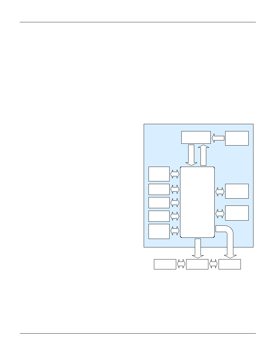
The PSoC architecture, as illustrated on the left, is comprised of
four main areas: PSoC Core, Digital System, Analog System,
and System Resources. Configurable global busing allows all
the device resources to be combined into a complete custom
system. The PSoC CY8C27x43 family can have up to five IO
ports that connect to the global digital and analog interconnects,
providing access to 8 digital blocks and 12 analog blocks.
The PSoC Core
The PSoC Core is a powerful engine that supports a rich fea-
ture set. The core includes a CPU, memory, clocks, and config-
urable GPIO (General Purpose IO).
The M8C CPU core is a powerful processor with speeds up to
24 MHz, providing a four MIPS 8-bit Harvard architecture micro-
Features
Powerful Harvard Architecture Processor
M8C Processor Speeds to 24 MHz
8x8 Multiply, 32-Bit Accumulate
Low Power at High Speed
3.0 to 5.25 V Operating Voltage
Operating Voltages Down to 1.0V Using On-
Chip Switch Mode Pump (SMP)
Industrial Temperature Range: -40∞C to +85∞C
Advanced Peripherals (PSoC Blocks)
12 Rail-to-Rail Analog PSoC Blocks Provide:
- Up to 14-Bit ADCs
- Up to 9-Bit DACs
- Programmable Gain Amplifiers
- Programmable Filters and Comparators
8 Digital PSoC Blocks Provide:
- 8- to 32-Bit Timers, Counters, and PWMs
- CRC and PRS Modules
- Up to 2 Full-Duplex UARTs
- Multiple SPI
TM
Masters or Slaves
- Connectable to all GPIO Pins
Complex Peripherals by Combining Blocks
Precision, Programmable Clocking
Internal 2.5% 24/48 MHz Oscillator
24/48 MHz with Optional 32 kHz Crystal
Optional External Oscillator, up to 24 MHz
Internal Oscillator for Watchdog and Sleep
Flexible On-Chip Memory
16K Bytes Flash Program Storage 50,000
Erase/Write Cycles
256 Bytes SRAM Data Storage
In-System Serial Programming (ISSP
TM
)
Partial Flash Updates
Flexible Protection Modes
EEPROM Emulation in Flash
Programmable Pin Configurations
25 mA Sink on all GPIO
Pull up, Pull down, High Z, Strong, or Open
Drain Drive Modes on all GPIO
Up to 12 Analog Inputs on GPIO
Four 30 mA Analog Outputs on GPIO
Configurable Interrupt on all GPIO
Additional System Resources
I
2
C
TM
Slave, Master, and Multi-Master to
400 kHz
Watchdog and Sleep Timers
User-Configurable Low Voltage Detection
Integrated Supervisory Circuit
On-Chip Precision Voltage Reference
Complete Development Tools
Free Development Software
(PSoCTM Designer)
Full-Featured, In-Circuit Emulator and
Programmer
Full Speed Emulation
Complex Breakpoint Structure
128K Bytes Trace Memory
DIGITAL SYSTEM
SRAM
256 Bytes
Interrupt
Controller
Sleep and
Watchdog
Multiple Clock Sources
(Includes IMO, ILO, PLL, and ECO)
Global Digital Interconnect
Global Analog Interconnect
PSoC
CORE
CPU Core (M8C)
SROM
Flash 16K
Digital
Block
Array
Multiply
Accum.
Switch
Mode
Pump
Internal
Voltage
Ref.
Digital
Clocks
POR and LVD
System Resets
Decimator
SYSTEM RESOURCES
ANALOG SYSTEM
Analog
Ref
Analog
Input
Muxing
I C
2
(2 Rows,
8 Blocks)
Port 4
Port 3
Port 2
Port 1 Port 0
Analog
Drivers
System Bus
Analog
Block
Array
(4 Columns,
12 Blocks)
Port 5

August 3, 2004
Document No. 38-12012 Rev. *I
2
CY8C27x43 Final Data Sheet
PSoCTM Overview
processor. The CPU utilizes an interrupt controller with 17 vec-
tors, to simplify programming of real time embedded events.
Program execution is timed and protected using the included
Sleep and Watch Dog Timers (WDT).
Memory encompasses 16 KB of Flash for program storage, 256
bytes of SRAM for data storage, and up to 2 KB of EEPROM
emulated using the Flash. Program Flash utilizes four protec-
tion levels on blocks of 64 bytes, allowing customized software
IP protection.
The PSoC device incorporates flexible internal clock genera-
tors, including a 24 MHz IMO (internal main oscillator) accurate
to 2.5% over temperature and voltage. The 24 MHz IMO can
also be doubled to 48 MHz for use by the digital system. A low
power 32 kHz ILO (internal low speed oscillator) is provided for
the Sleep timer and WDT. If crystal accuracy is desired, the
ECO (32.768 kHz external crystal oscillator) is available for use
as a Real Time Clock (RTC) and can optionally generate a crys-
tal-accurate 24 MHz system clock using a PLL. The clocks,
together with programmable clock dividers (as a System
Resource), provide the flexibility to integrate almost any timing
requirement into the PSoC device.
PSoC GPIOs provide connection to the CPU, digital and analog
resources of the device. Each pin's drive mode may be selected
from eight options, allowing great flexibility in external interfac-
ing. Every pin also has the capability to generate a system inter-
rupt on high level, low level, and change from last read.
The Digital System
The Digital System is composed of 8 digital PSoC blocks. Each
block is an 8-bit resource that can be used alone or combined
with other blocks to form 8, 16, 24, and 32-bit peripherals, which
are called user module references.
Digital System Block Diagram
Digital peripheral configurations include those listed below.
PWMs (8 to 32 bit)
PWMs with Dead band (8 to 32 bit)
Counters (8 to 32 bit)
Timers (8 to 32 bit)
UART 8 bit with selectable parity (up to 2)
SPI master and slave (up to 2)
I2C slave and master (1 available as a System Resource)
Cyclical Redundancy Checker/Generator (8 to 32 bit)
IrDA (up to 2)
Pseudo Random Sequence Generators (8 to 32 bit)
The digital blocks can be connected to any GPIO through a
series of global buses that can route any signal to any pin. The
buses also allow for signal multiplexing and for performing logic
operations. This configurability frees your designs from the con-
straints of a fixed peripheral controller.
Digital blocks are provided in rows of four, where the number of
blocks varies by PSoC device family. This allows you the opti-
mum choice of system resources for your application. Family
resources are shown in the table titled
"PSoC Device Charac-
teristics" on page 3
.
The Analog System
The Analog System is composed of 12 configurable blocks,
each comprised of an opamp circuit allowing the creation of
complex analog signal flows. Analog peripherals are very flexi-
ble and can be customized to support specific application
requirements. Some of the more common PSoC analog func-
tions (most available as user modules) are listed below.
Analog-to-digital converters (up to 4, with 6- to 14-bit resolu-
tion, selectable as Incremental, Delta Sigma, and SAR)
Filters (2, 4, 6, and 8 pole band-pass, low-pass, and notch)
Amplifiers (up to 4, with selectable gain to 48x)
Instrumentation amplifiers (up to 2, with selectable gain to
93x)
Comparators (up to 4, with 16 selectable thresholds)
DACs (up to 4, with 6- to 9-bit resolution)
Multiplying DACs (up to 4, with 6- to 9-bit resolution)
High current output drivers (four with 30 mA drive as a Core
Resource)
1.3V reference (as a System Resource)
DTMF dialer
Modulators
Correlators
Peak detectors
Many other topologies possible
DIGITAL SYSTEM
To System Bus
Digital Clocks
From Core
Digital PSoC Block Array
To Analog
System
8
Ro
w I
n
p
u
t
C
onf
i
gur
at
i
o
n
Ro
w O
u
t
p
u
t
C
onf
i
gur
at
i
o
n
8
8
8
Row 1
DBB10
DBB11
DCB12
DCB13
R
o
w
I
nput
C
onf
i
g
ur
at
i
o
n
4
4
R
o
w
O
u
t
put
C
onf
i
gur
ati
o
n
Row 0
DBB00
DBB01
DCB02
DCB03
4
4
GIE[7:0]
GIO[7:0]
GOE[7:0]
GOO[7:0]
Global Digital
Interconnect
Port 4
Port 3
Port 2
Port 1
Port 0
Port 5

August 3, 2004
Document No. 38-12012 Rev. *I
3
CY8C27x43 Final Data Sheet
PSoCTM Overview
Analog blocks are provided in columns of three, which includes
one CT (Continuous Time) and two SC (Switched Capacitor)
blocks, as shown in the figure below.
Analog System Block Diagram
Additional System Resources
System Resources, some of which have been previously listed,
provide additional capability useful to complete systems. Addi-
tional resources include a multiplier, decimator, switch mode
pump, low voltage detection, and power on reset. Brief state-
ments describing the merits of each system resource are pre-
sented below.
Digital clock dividers provide three customizable clock fre-
quencies for use in applications. The clocks can be routed to
both the digital and analog systems. Additional clocks can be
generated using digital PSoC blocks as clock dividers.
A multiply accumulate (MAC) provides a fast 8-bit multiplier
with 32-bit accumulate, to assist in both general math as well
as digital filters.
The decimator provides a custom hardware filter for digital
signal processing applications including the creation of Delta
Sigma ADCs.
The I2C module provides 100 and 400 kHz communication
over two wires. Slave, master, and multi-master modes are
all supported.
Low Voltage Detection (LVD) interrupts can signal the appli-
cation of falling voltage levels, while the advanced POR
(Power On Reset) circuit eliminates the need for a system
supervisor.
An internal 1.3V reference provides an absolute reference for
the analog system, including ADCs and DACs.
An integrated switch mode pump (SMP) generates normal
operating voltages from a single 1.2V battery cell, providing a
low cost boost converter.
PSoC Device Characteristics
Depending on your PSoC device characteristics, the digital and
analog systems can have 16, 8, or 4 digital blocks and 12, 6, or
3 analog blocks. The following table lists the resources
available for specific PSoC device groups. The PSoC device
covered by this data sheet is shown in the second row of the
table.
ACB00
ACB01
Block Array
Array Input Configuration
ACI1[1:0]
ACI2[1:0]
ACB02
ACB03
ASC12
ASD13
ASD22
ASC23
ASD20
ACI0[1:0]
ACI3[1:0]
P0[6]
P0[4]
P0[2]
P0[0]
P2[2]
P2[0]
P2[6]
P2[4]
Re
f
I
n
AGNDI
n
P0[7]
P0[5]
P0[3]
P0[1]
P2[3]
P2[1]
Reference
Generators
AGNDIn
RefIn
Bandgap
RefHi
RefLo
AGND
ASD11
ASC21
ASC10
Interface to
Digital System
M8C Interface (Address Bus, Data Bus, Etc.)
Analog Reference
PSoC Device Characteristics
PSoC Part
Number
Dig
i
t
a
l
IO
Dig
i
t
a
l
Ro
ws
Dig
i
t
a
l
Bl
o
c
k
s
A
n
a
l
og
I
npu
t
s
A
n
a
l
og
Ou
tp
u
t
s
A
n
a
l
og
Co
lu
m
n
s
A
n
a
l
og
Bl
o
c
k
s
CY8C29x66
up to
64
4
16
12
4
4
12
CY8C27x43
up to
44
2
8
12
4
4
12
CY8C24x23
up to
24
1
4
12
2
2
6
CY8C24x23A
up to
24
1
4
12
2
2
6
CY8C22x13
up to
16
1
4
8
1
1
3
August 3, 2004
Document No. 38-12012 Rev. *I
4
CY8C27x43 Final Data Sheet
PSoCTM Overview
Getting Started
The quickest path to understanding the PSoC silicon is by read-
ing this data sheet and using the PSoC Designer Integrated
Development Environment (IDE). This data sheet is an over-
view of the PSoC integrated circuit and presents specific pin,
register, and electrical specifications. For in-depth information,
along with detailed programming information, reference the
PSoCTM Mixed Signal Array Technical Reference Manual.
For up-to-date Ordering, Packaging, and Electrical Specification
information, reference the latest PSoC device data sheets on
the web at
http://www.cypress.com/psoc.
Development Kits
Development Kits are available from the following distributors:
Digi-Key, Avnet, Arrow, and Future. The Cypress Online Store
at
http://www.onfulfillment.com/cypressstore/
contains develop-
ment kits, C compilers, and all accessories for PSoC develop-
ment. Click on PSoC (Programmable System-on-Chip) to view
a current list of available items.
Tele-Training
Free PSoC "Tele-training" is available for beginners and taught
by a live marketing or application engineer over the phone. Five
training classes are available to accelerate the learning curve
including introduction, designing, debugging, advanced design,
advanced analog, as well as application-specific classes cover-
ing topics like PSoC and the LIN bus. For days and times of the
tele-training, see
http://www.cypress.com/support/training.cfm
.
Consultants
Certified PSoC Consultants offer everything from technical
assistance to completed PSoC designs. To contact or become a
PSoC Consultant, go to the following Cypress support web site:
http://www.cypress.com/support/cypros.cfm
.
Technical Support
PSoC application engineers take pride in fast and accurate
response. They can be reached with a 4-hour guaranteed
response at
http://www.cypress.com/support/login.cfm
.
Application Notes
A long list of application notes will assist you in every aspect of
your design effort. To locate the PSoC application notes, go to
http://www.cypress.com/design/results.cfm
.
Development Tools
The Cypress MicroSystems PSoC Designer is a Microsoft
Æ
Windows-based, integrated development environment for the
Programmable System-on-Chip (PSoC) devices. The PSoC
Designer IDE and application runs on Windows NT 4.0, Win-
dows 2000, Windows Millennium (Me), or Windows XP. (Refer-
ence the PSoC Designer Functional Flow diagram below.)
PSoC Designer helps the customer to select an operating con-
figuration for the PSoC, write application code that uses the
PSoC, and debug the application. This system provides design
database management by project, an integrated debugger with
In-Circuit Emulator, in-system programming support, and the
CYASM macro assembler for the CPUs.
PSoC Designer also supports a high-level C language compiler
developed specifically for the devices in the family.
PSoC Designer Subsystems
C
o
m
m
and
s
Res
u
l
t
s
PSoC
TM
Designer
Core
Engine
PSoC
Configuration
Sheet
Manufacturing
Information
File
Device
Database
Importable
Design
Database
Device
Programmer
Graphical Designer
Interface
Context
Sensitive
Help
Emulation
Pod
In-Circuit
Emulator
Project
Database
Application
Database
User
Modules
Library
PSoC
TM
Designer

August 3, 2004
Document No. 38-12012 Rev. *I
5
CY8C27x43 Final Data Sheet
PSoCTM Overview
PSoC Designer Software Subsystems
Device Editor
The Device Editor subsystem allows the user to select different
onboard analog and digital components called user modules
using the PSoC blocks. Examples of user modules are ADCs,
DACs, Amplifiers, and Filters.
The device editor also supports easy development of multiple
configurations and dynamic reconfiguration. Dynamic configu-
ration allows for changing configurations at run time.
PSoC Designer sets up power-on initialization tables for
selected PSoC block configurations and creates source code
for an application framework. The framework contains software
to operate the selected components and, if the project uses
more than one operating configuration, contains routines to
switch between different sets of PSoC block configurations at
run time. PSoC Designer can print out a configuration sheet for
a given project configuration for use during application pro-
gramming in conjunction with the Device Data Sheet. Once the
framework is generated, the user can add application-specific
code to flesh out the framework. It's also possible to change the
selected components and regenerate the framework.
Design Browser
The Design Browser allows users to select and import precon-
figured designs into the user's project. Users can easily browse
a catalog of preconfigured designs to facilitate time-to-design.
Examples provided in the tools include a 300-baud modem, LIN
Bus master and slave, fan controller, and magnetic card reader.
Application Editor
In the Application Editor you can edit your C language and
Assembly language source code. You can also assemble, com-
pile, link, and build.
Assembler.
The macro assembler allows the assembly code
to be merged seamlessly with C code. The link libraries auto-
matically use absolute addressing or can be compiled in relative
mode, and linked with other software modules to get absolute
addressing.
C Language Compiler.
A C language compiler is available
that supports Cypress MicroSystems' PSoC family devices.
Even if you have never worked in the C language before, the
product quickly allows you to create complete C programs for
the PSoC family devices.
The embedded, optimizing C compiler provides all the features
of C tailored to the PSoC architecture. It comes complete with
embedded libraries providing port and bus operations, standard
keypad and display support, and extended math functionality.
Debugger
The PSoC Designer Debugger subsystem provides hardware
in-circuit emulation, allowing the designer to test the program in
a physical system while providing an internal view of the PSoC
device. Debugger commands allow the designer to read and
program and read and write data memory, read and write IO
registers, read and write CPU registers, set and clear break-
points, and provide program run, halt, and step control. The
debugger also allows the designer to create a trace buffer of
registers and memory locations of interest.
Online Help System
The online help system displays online, context-sensitive help
for the user. Designed for procedural and quick reference, each
functional subsystem has its own context-sensitive help. This
system also provides tutorials and links to FAQs and an Online
Support Forum to aid the designer in getting started.
Hardware Tools
In-Circuit Emulator
A low cost, high functionality ICE (In-Circuit Emulator) is avail-
able for development support. This hardware has the capability
to program single devices.
The emulator consists of a base unit that connects to the PC by
way of the parallel or USB port. The base unit is universal and
will operate with all PSoC devices. Emulation pods for each
device family are available separately. The emulation pod takes
the place of the PSoC device in the target board and performs
full speed (24 MHz) operation.