 | –≠–ª–µ–∫—Ç—Ä–æ–Ω–Ω—ã–π –∫–æ–º–ø–æ–Ω–µ–Ω—Ç: CY7C68023 | –°–∫–∞—á–∞—Ç—å:  PDF PDF  ZIP ZIP |

EZ-USB NX2LPTM USB 2.0 NAND Flash Controller
CY7C68023/CY7C68024
Cypress Semiconductor Corporation
∑
3901 North First Street
∑
San Jose
,
CA 95134
∑
408-943-2600
Document #: 38-08055 Rev. *A
Revised March 16, 2005
1.0
Features
∑ High (480-Mbps) or full (12-Mbps) speed USB support
∑ Both common NAND page sizes supported
-- 512bytes ≠Up to 1Gbit Capacity
-- 2K bytes ≠Up to 8Gbit Capacity
∑ 8 chip enable pins
-- Up to 8 NAND Flash single-device chips
-- Up to 4 NAND Flash dual-device chips
∑ Industry standard ECC NAND Flash correction
-- 1-bit per 256 correction
-- 2-bit error detection
∑ Industry standard (SmartMedia) page management for
wear leveling algorithm, bad block handling, and Physical
to Logical management.
∑ Supports 8-bit NAND Flash interfaces
∑ Supports 30ns, 50ns, 100ns NAND Flash timing
∑ Complies with USB Mass Storage Class Specification rev
1.0
∑ CY7C68024 complies with USB 2.0 Specification for Bus-
Powered Devices (TID# 40460274)
∑ 43-mA Typical Active Current
∑ Space-saving and lead-free 56-QFN package (8mm
◊
8mm)
∑ Support for board-level manufacturing test via USB
interface
∑ 3.3V NAND Flash operation
∑ NAND Flash power management support
2.0
Introduction
The EZ-USB NX2LP
TM
(
NX2LP
)
implements a USB 2.0 NAND
Flash controller. This controller adheres to the Mass Storage
Class Bulk-Only Transport Specification. The USB port of the
NX2LP is connected to a host computer directly or via the
downstream port of a USB hub. Host software issues
commands and data to the NX2LP and receives status and
data from the NX2LP using standard USB protocol.
The NX2LP supports industry leading 8-bit NAND Flash inter-
faces and both common NAND page sizes of 512 and 2k
bytes. Eight chip enable pins allow the NX2LP to be connected
to up to eight single- or four dual-device NAND Flash chips.
Certain NX2LP features are configurable, enabling the NX2LP
to meet the needs of different designs' requirements.
Figure 1-1. NX2LP Block Diagram
USB 2.0
Xceiver
Smart HS/
FS USB
Engine
NAND Flash
Interface
Logic
8-bit Data Bus
NAND Control Signals
EZ-USB NX2LP
Internal Control Logic
PLL
24 MHz
Xtal
VBUS
D+
D-
Data
Control
Chip Reset
LED1#
LED2#
Write Protect
Chip Enable Signals
CY7C68023/CY7C68024
Document #: 38-08055 Rev. *A
Page 2 of 9
3.0
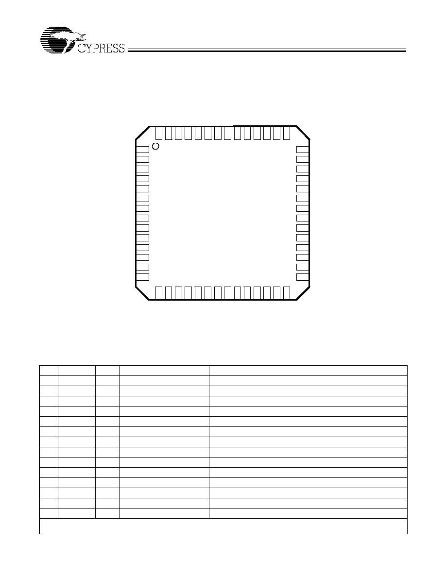
Pin Assignments
3.1
Pin Diagram
Figure 3-1. 56-pin QFN
3.2
Pin Descriptions
Pin
Name
Type
Default State at Start-up
Description
1
R_B1#
[1]
I
Z
Ready/Busy 1 (2.2k to 4k pull-up resistor is required)
2
R_B2#
I
Z
Ready/Busy 2 (2.2k to 4k pull-up resistor is required)
3
AVCC
PWR
PWR
Analog 3.3V supply
4
XTALOUT
Xtal
N/A
Crystal output
5
XTALIN
Xtal
N/A
Crystal input
6
AGND
GND
GND
Ground
7
AVCC
PWR
PWR
Analog 3.3V supply
8
DPLUS
I/O
Z
USB D+
9
DMINUS
I/O
Z
USB D-
10
AGND
GND
GND
Ground
11
VCC
PWR
PWR
3.3V supply
12
GND
GND
GND
Ground
13
N/C
N/A
N/A
No connect
14
GND
GND
GND
Ground
Note:
1.
A # sign after the pin name indicates that it is an active LOW signal.
RESET#
GND
N/C
N/C
WP_SW#
WP_NF#
LED2#
LED1#
ALE
CLE
VCC
RE1#
RE0#
WE#
R_B1#
R_B2#
AVCC
XTALOUT
XTALIN
AGND
AVCC
DPLUS
DMINUS
AGND
VCC
GND
N/C
GND
15
16
17
18
19
20
21
22
23
24
25
26
27
28
Re
s
e
rv
e
d
Re
s
e
rv
e
d
VC
C
DD
0
DD
1
DD
2
DD
3
DD
4
DD
5
DD
6
DD
7
GND
VC
C
GND
42
41
40
39
38
37
36
35
34
33
32
31
30
29
56
55
54
53
52
51
50
49
48
47
46
45
44
43
1
2
3
4
5
6
7
8
9
10
11
12
13
14
GND
VC
C
N/
C
GND
CE
7
#
CE
6
#
CE
5
#
CE
4
#
CE
3
#
CE
2
#
CE
1
#
CE
0
#
Re
s
e
rv
e
d
VC
C
EZ-USB NX2LP
56-pin QFN
CY7C68023/CY7C68024
Document #: 38-08055 Rev. *A
Page 3 of 9
15
Reserved
N/A
N/A
Must be tied HIGH (no pull-up resistor required)
16
Reserved
N/A
N/A
Must be tied HIGH (no pull-up resistor required)
17
VCC
PWR
PWR
3.3V supply
18
DDO
I/O
Z
Data 0
19
DD1
I/O
Z
Data 1
20
DD2
I/O
Z
Data 2
21
DD3
I/O
Z
Data 3
22
DD4
I/O
Z
Data 4
23
DD5
I/O
Z
Data 5
24
DD6
I/O
Z
Data 6
25
DD7
I/O
Z
Data 7
26
GND
GND
GND
Ground
27
VCC
PWR
PWR
3.3V supply
28
GND
GND
GND
Ground
29
WE#
O
H
Write enable
30
RE0#
O
H
Read Enable 0
31
RE1#
O
H
Read Enable 1
32
VCC
PWR
PWR
3.3V supply
33
CLE
O
Z
Command latch enable
34
ALE
O
Z
Address latch enable
35
LED1#
O
Z
Data activity LED sink
36
LED2#
O
Z
Chip active LED sink
37
WP_NF#
O
Z
Write-protect NAND Flash
38
WP_SW#
I
Z
Write-protect switch input
39
N/C
N/A
N/A
No connect
40
N/C
N/A
N/A
No connect
41
GND
GND
GND
Ground
42
RESET#
I
Z
NX2LP chip reset
43
VCC
PWR
PWR
3.3V supply
44
Reserved
N/A
N/A
Must be tied HIGH
45
CE0#
O
Z
Chip enable 0
46
CE1#
O
Z
Chip enable 1
47
CE2#
O
Z
Chip enable 2
48
CE3#
O
Z
Chip enable 3
49
CE4#
O
Z
Chip enable 4
50
CE5#
O
Z
Chip enable 5
51
CE6#
O
Z
Chip enable 6
52
CE7#
O
Z
Chip enable 7
53
GND
GND
GND
Ground
54
N/C
N/A
N/A
No connect
55
VCC
PWR
PWR
3.3V supply
56
GND
GND
GND
Ground
3.2
Pin Descriptions
(continued)
Pin
Name
Type
Default State at Start-up
Description

CY7C68023/CY7C68024
Document #: 38-08055 Rev. *A
Page 4 of 9
3.3
Additional Pin Descriptions
3.3.1
DPLUS, DMINUS
DPLUS and DMINUS are the USB signaling pins, and they
should be tied to the D+ and D≠ pins of the USB connector.
Because they operate at high frequencies, the USB signals
require special consideration when designing the layout of the
PCB. General guidelines are given at the end of this
document.
3.3.2
XTALIN, XTALOUT
The NX2LP requires a 24-MHz (
±
100ppm) signal to derive
internal timing. Typically, a 24-MHz (20-pF, 500-uW, parallel-
resonant fundamental mode) crystal is used, but a 24-MHz
square wave from another source can also be used. If a crystal
is used, connect its pins to XTALIN and XTALOUT, and also
through 12-pF capacitors to GND. If an alternate clock source
is used, apply it to XTALIN and leave XTALOUT open.
3.3.3
Data[7-0]
The Data[7-0] I/O pins provide an 8-bit interface to a NAND
Flash device. These pins are used to transfer address,
command, and read/write data between the NX2LP and NAND
Flash.
3.3.4
R_B[2-1]#
The Ready/Busy input pins are used to determine the state of
the currently selected NAND Flash device. These pins must
be pulled HIGH through a 2k-4k resistor. These pins are pulled
LOW by the NAND Flash when it is busy.
3.3.5
WE#
The Write Enable output pin is used by the NAND Flash to
latch commands, address, and data during the rising edge of
the pulse.
3.3.6
RE[1-0]#
The Read Enable output pins are used to control the data flow
from the NAND Flash devices. The device presents valid data
and will increment its internal column address counter by one
step on each falling edge of the Read Enable pulse. A 10k pull-
up is an option For RE1-0#.
3.3.7
CLE
The Command Latch Enable output pin is used to indicate that
the data on the I/O bus is a command. The data is latched into
the NAND Flash control register on the rising edge of WE#
when CLE is HIGH.
3.3.8
ALE
The Address Latch Enable output pin is used to indicate that
the data on the I/O bus is an address. The data is latched into
the NAND Flash address register on the rising edge of WE#
when ALE is HIGH.
3.3.9
LED1#
The Data Activity LED output pin is used to indicate data
transfer activity. LED1# is asserted LOW at the beginning of a
data transfer, and set to a high-Z state when the transfer is
complete. If this functionality is not utilized, leave LED1#
floating.
3.3.10
LED2#
The Chip Active LED output pin is used to indicate proper
device operation. LED2# is asserted LOW when the NX2LP is
powered and initialized. It is placed in a high-Z state under all
other conditions. If this functionality is not utilized, leave
LED2# floating.
3.3.11
WP_NF#
The Write-protect NAND Flash output pin is used to control the
write-protect pins on NAND Flash devices. This pin should be
tied to the Write Protect pins of the NAND Flash devices. If
WP_SW# is asserted LOW during a data transfer, or if internal
operations are still pending, the NX2LP will wait until the
operation is complete before asserting WP_NF# to ensure that
there is no data loss or risk of OS error.
3.3.12
WP_SW#
The Write-protect Switch input pin is used to select whether or
not NAND Flash write-protection is enabled by the NX2LP.
When the pin is asserted LOW, the NX2LP will report to the
host that the NAND Flash is write-protected, the WP_NF# will
be driven LOW, and any attempts to write to the configuration
data memory area will be blocked by the NX2LP. If this pin is
asserted LOW during a data transfer, or if internal operations
are still pending, the NX2LP will wait until the operation is
complete before asserting WP_NF# to ensure that there is no
data loss or risk of OS error.
3.3.13
CE[7-0]#
The Chip Enable output pins are used to select the NAND
Flash that the NX2LP will interface. Unused Chip Enable pins
should be left floating.
3.3.14
RESET#
Asserting RESET# for 10 ms will reset the NX2LP. A reset
and/or watchdog chip is recommended to ensure that startup
and brownout conditions are properly handled.
Figure 3-2. XTALIN, XTALOUT Diagram
24MHz Xtal
12pF
XTALIN
XTALOUT
12pF
12pF capacitor
values assume a
trace capacitance
of 3pF per side on a
four-layer FR4 PCB

CY7C68023/CY7C68024
Document #: 38-08055 Rev. *A
Page 5 of 9
4.0
Applications
The NX2LP is a high-speed USB 2.0 peripheral device that
connects NAND Flash devices to a USB host using the USB
Mass Storage Class protocol.
4.1
Additional Resources
∑ CY3685 EZ-USB NX2LP Development Kit
∑ CY4618 EZ-USB NX2LP Reference Design Kit
∑ USB Specification version 2.0
∑ USB Mass Storage Class Bulk Only Transport Specification,
http://www.usb.org/developers/data/devclass/
usbmassbulk_10.pdf.
5.0
Functional Overview
5.1
USB Signaling Speed
The NX2LP operates at two of the three rates defined in the
USB Specification Revision 2.0 dated April 27, 2000:
∑ Full speed, with a signaling bit rate of 12 Mbits/sec
∑ High speed, with a signaling bit rate of 480 Mbits/sec.
The NX2LP does not support the low-speed signaling rate of
1.5 Mbits/sec.
5.2
NAND Flash Interface
During normal operation the NX2LP supports an 8-bit I/O
interface, eight chip enable pins, and other control signals
compatible with industry standard NAND Flash devices.
6.0
Enumeration
During the start-up sequence, internal logic checks for the
presence of NAND Flash with valid configuration data in the
configuration data memory area. If valid configuration data is
found, the NX2LP uses the values stored in NAND Flash to
configure the USB descriptors for normal operation as a USB
mass storage device. If no NAND Flash is detected, or if no
valid configuration data is found in the configuration data
memory area, the NX2LP uses the default values from internal
ROM space for manufacturing mode operation. The two
modes of operation are described in sections 6.1 and 6.2
below.
6.1
Normal Operation Mode
In Normal Operation Mode, the NX2LP behaves as a USB 2.0
Mass Storage Class NAND Flash controller. This includes all
typical USB device states (powered, configured, etc.). The
USB descriptors are returned according to the data stored in
the configuration data memory area. Normal read and write
access to the NAND Flash is available in this mode.
6.2
Manufacturing Mode
In Manufacturing mode, the NX2LP enumerates using the
default descriptors and configuration data that are stored in
internal ROM. This mode allows for first-time programming of
the configuration data memory area, as well as board-level
manufacturing tests.
A unique USB serial number is required for each device in
order to comply with the USB Mass Storage specification.
Also, Cypress requires designers to use their own Vendor ID
for final products. The Vendor ID is obtained through regis-
tration with the USB Implementor's Forum (USB-IF), and the
Product ID is determined by the designer.
Cypress provides all the software tools and drivers necessary
for properly programming and testing the NX2LP. Please refer
to the documentation in the development or reference design
kit for more information on these topics.
NAND Flash
Programmed?
Load Default
Descriptors and
Configuration Data
Manufacturing
Mode
Load Custom
Descriptors and
Configuration Data
Enumerate As
USB Mass
Storage Device
Normal Operation
Mode
Start-up
Enumerate As
Generic NX2LP
Device
NAND Flash
Present?
No
Yes
Yes
No
Figure 6-1. NX2LP Enumeration Process