 | ÐлекÑÑоннÑй компоненÑ: CY7C63101 | СкаÑаÑÑ:  PDF PDF  ZIP ZIP |
Äîêóìåíòàöèÿ è îïèñàíèÿ www.docs.chipfind.ru

PRELIMINARY
fax id: 3401
CY7C63000/CY7C63001
CY7C63100/CY7C63101
CY7C63200/CY7C63201
Cypress Semiconductor Corporation
·
3901 North First Street
·
San Jose
·
CA 95134
·
408-943-2600
October 1996 - Revised June 26, 1997
1CY 7C63 00 0
CY7C63000
CY7C63001
CY7C63100
CY7C63101
CY7C63200
CY7C63201
Universal Serial Bus Microcontroller

CY7C63000/CY7C63001
CY7C63100/CY7C63101
CY7C63200/CY7C63201
PRELIMINARY
2
TABLE OF CONTENTS
1.0 FEATURES ..................................................................................................................................... 4
2.0 FUNCTIONAL OVERVIEW ............................................................................................................. 4
3.0 PIN DEFINITIONS ........................................................................................................................... 6
4.0 PIN DESCRIPTION ......................................................................................................................... 7
5.0 FUNCTIONAL DESCRIPTION ........................................................................................................ 7
5.1 Memory Organization .................................................................................................................... 7
5.1.1 Program Memory Organization ........................................................................................................... 7
5.1.2 Security Fuse Bit .................................................................................................................................... 7
5.1.3 Data Memory Organization ................................................................................................................... 9
5.2 I/O Register Summary ................................................................................................................... 9
5.3 Reset .............................................................................................................................................10
5.3.1 Power-On Reset (POR) ....................................................................................................................... 10
5.3.2 Watch Dog Reset (WDR) .................................................................................................................... 11
5.3.3 USB Bus Reset ................................................................................................................................... 11
5.4 On-chip Timer ..............................................................................................................................11
5.5 General Purpose I/O Ports ..........................................................................................................12
5.6 Instant-on Feature (Suspend Mode) ..........................................................................................14
5.7 XTALIN/XTALOUT ........................................................................................................................14
5.8 Interrupts ......................................................................................................................................15
5.8.1 Interrupt Latency ................................................................................................................................ 16
5.8.2 GPIO Interrupt ..................................................................................................................................... 16
5.8.3 USB Interrupt ...................................................................................................................................... 17
5.8.4 Timer Interrupt .................................................................................................................................... 17
5.8.5 Wake-up Interrupt ............................................................................................................................... 17
5.9 USB Engine ..................................................................................................................................17
5.9.1 USB Enumeration Process ................................................................................................................ 18
5.9.2 End Point 0 .......................................................................................................................................... 18
5.9.2.1 End Point 0 Receive .................................................................................................................................... 18
5.9.2.2 End Point 0 Transmit ................................................................................................................................... 18
5.9.3 End Point 1 .......................................................................................................................................... 20
5.9.3.1 End Point 1 Transmit ................................................................................................................................... 20
5.9.4 USB Status and Control ..................................................................................................................... 20
5.10 Instruction Set Summary ..........................................................................................................21
6.0 ABSOLUTE MAXIMUM RATINGS ...............................................................................................22
7.0 DC CHARACTERISTICS ..............................................................................................................22
8.0 SWITCHING CHARACTERISTICS ...............................................................................................23
9.0 ORDERING INFORMATION .........................................................................................................24
10.0 PACKAGE DIAGRAMS ..............................................................................................................25

CY7C63000/CY7C63001
CY7C63100/CY7C63101
CY7C63200/CY7C63201
PRELIMINARY
3
TABLE OF FIGURES
Figure 5-1. Program Memory Space ................................................................................................... 8
Figure 5-2. Data Memory Space .......................................................................................................... 9
Figure 5-3. Status and Control Register (Address 0xFF) ................................................................ 10
Figure 5-4. Watch Dog Reset (WDR) ................................................................................................. 11
Figure 5-5. Timer Register (Address 0x23)....................................................................................... 11
Figure 5-6. Timer Block Diagram....................................................................................................... 12
Figure 5-7. Port 0 Data Register (Address 0x00) ............................................................................. 12
Figure 5-8. Port 1 Data Register (Address 0x01) ............................................................................. 12
Figure 5-9. Block Diagram of an I/O Line.......................................................................................... 13
Figure 5-10. Port 0 Pull-Up Register (Address 0x08)....................................................................... 13
Figure 5-11. Port 1 Pull-Up Register (Address 0x09)....................................................................... 13
Figure 5-12. Port Isink Register for One GPIO Line......................................................................... 14
Figure 5-13. The Cext Register (Address 0x22) ............................................................................... 14
Figure 5-14. Clock Oscillator On-chip Circuit .................................................................................. 14
Figure 5-15. Global Interrupt Enable Register (Address 0x20)....................................................... 15
Figure 5-16. Interrupt Controller Logic Block Diagram ................................................................... 15
Figure 5-17. Port 0 Interrupt Enable Register (Address 0x04)........................................................ 16
Figure 5-18. Port 1 Interrupt Enable Register (Address 0x05)........................................................ 16
Figure 5-19. GPIO Interrupt Logic Block Diagram ........................................................................... 17
Figure 5-20. USB Device Address Register (Address 0x12) ........................................................... 18
Figure 5-21. USB End Point 0 RX Register (Address 0x14) ............................................................ 18
Figure 5-22. USB Engine Response to SETUP and OUT transactions on End Point 0 ................ 19
Figure 5-23. USB End Point 0 TX Configuration Register (Address 0x10) .................................... 19
Figure 5-24. USB End Point 1 TX Configuration Register (Address 0x11) .................................... 20
Figure 5-25. USB Status and Control Register (Address 0x13)...................................................... 20
Figure 8-1. Clock Timing .................................................................................................................... 24
Figure 8-2. USB Data Signal Timing.................................................................................................. 24
TABLE OF TABLES
Table 5-1. I/O Register Summary......................................................................................................... 9
Table 5-2. Output Control Truth Table ..............................................................................................13
Table 5-3. Interrupt Vector Assignments..........................................................................................16
Table 5-4. Instruction Set Map ...........................................................................................................21
2

CY7C63000/CY7C63001
CY7C63100/CY7C63101
CY7C63200/CY7C63201
PRELIMINARY
4
1.0
Features
· Low-cost solution for low-speed USB peripherals such as mouse, joystick, and gamepad
· USB Specification Compliance
-- Conforms to USB 1.5 Mbps Specification, Version 1.0
-- Conforms to USB HID Specification, Version 1.0
-- Supports 1 device address and 2 endpoints
· 8-bit RISC microcontroller
-- Harvard architecture
-- 6 MHz external ceramic resonator or clock crystal
-- 12 MHz internal operation
-- USB optimized instruction set
· Internal memory
-- 128 bytes of RAM
-- 2K bytes of EPROM (CY7C63000, CY7C63100, CY7C63200)
-- 4K bytes of EPROM (CY7C63001, CY7C63101, CY7C63201)
· I/O ports
-- Integrated USB transceivers
-- Up to 16 Schmitt trigger I/O pins with internal pull-up
-- Up to 8 I/O pins with LED drive capability
-- Special purpose I/O mode supports optimization of photo transistor and LED in mouse application
-- Maskable Interrupts on all I/O pins
· 8-bit free-running timer
· Watchdog timer (WDT)
· Internal power-on reset (POR)
· Improved output drivers to reduce EMI
· Operating voltage from 4.0V to 5.25VDC
· Operating temperature from 0 to 70 degree Celsius
· Available in space saving and low cost 18-pin PDIP, 20-pin PDIP, 20-pin SOIC, and 24-pin SOIC packages
· Windowed packages also available to support program development: 18, 20, and 24-pin Windowed CerDIP
· Industry standard programmer support
2.0
Functional Overview
The CY7C63xxx is a family of 8-bit RISC One Time Programmable (OTP) microcontrollers with a built-in 1.5-Mbps USB serial
interface engine. The microcontroller features 35 instructions which are optimized for USB applications. There is 128 bytes of
onboard RAM available incorporated into each microcontroller. The Cypress USB Controller accepts a 6 MHz ceramic resonator
or a 6 MHz crystal as its clock source. This clock is doubled within the chip to provide a 12 MHz clock for the microprocessor.
The microcontroller features two ports of up to sixteen general purpose I/Os (GPIOs). Each GPIO pin can be used to generate
an interrupt to the microcontroller. Additionally, all pins in Port 1 are equipped with programmable drivers strong enough to drive
LEDs. The GPIO ports feature low EMI emissions as a result of controlled rise and fall times, and unique output driver circuits in
the microcontroller. The Cypress microcontrolles have a range of GPIOs to fit various applications; the CY7C630xx has twelve
GPIO, the CY7C631xx has sixteen GPIO, and the CY7C632xx has ten GPIO. Notice that each part has eight `low-current' ports
(Port 0)with the remaining ports (Port 1) being `high-current'
The twelve GPIO CY7C6300x is available in is a 20-pin PDIP (-PC), 20-pin SOIC (-SC), and a 20-pin Windowed CerDIP. The
sixteen GPIO CY7C6310x is available in a 24-pin SOIC (-SC) and a 24-pin Windowed CerDIP (-SC). The ten GPIO CY7C6320x
is available in an 18-pin PDIP (-PC) and an 18-pin Windowed CerDIP (-WC).
CY7C63000/CY7C63001
CY7C63100/CY7C63101
CY7C63200/CY7C63201
PRELIMINARY
5
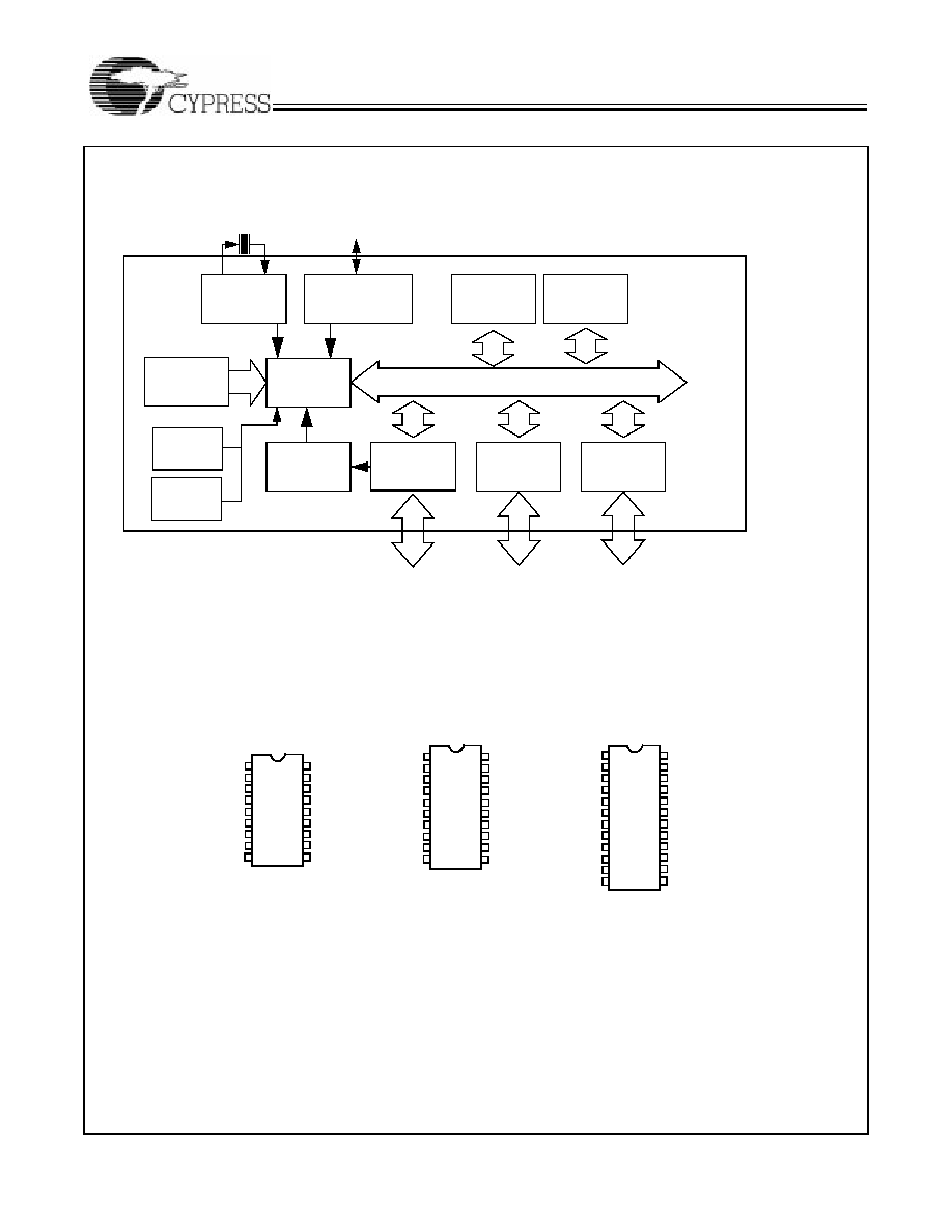
.
Pin Configurations (Top View)
Logic Block Diagram
63111
USB
D+,D
PORT
P0.0P0.7
Interrupt
Controller
0
PORT
P1.0P1.7
1
8-bit
RISC
OSC
RAM
128 Byte
EPROM
2K/4K Byte
1
2
3
4
5
6
7
9
13
14
15
16
17
18
20
19
P0.0
P0.1
P0.2
P0.3
P1.0
P1.2
VSS
CEXT
P0.4
P1.1
P0.6
P0.7
D+
P1.3
D-
VCC
DIP/SOIC/
12
P0.5
8
VPP
XTALIN
XTALOUT
10
11
core
Power
8-bit
Timer
on Reset
Engine
Watch
Timer
1
2
3
4
5
6
7
9
11
12
13
14
15
16
18
17
P0.0
P0.1
P0.2
P0.3
P1.0
VSS
VPP
XTALIN
P0.4
P1.1
P0.6
P0.7
D-
D+
VCC
XTALOUT
DIP/
10
P0.5
8
CEXT
Dog
6 MHz
RESONATOR
1
2
3
4
5
6
9
11
15
16
17
18
19
20
22
21
P0.0
P0.1
P0.2
P0.3
P1.0
P1.2
VSS
CEXT
P0.6
P1.5
P1.1
P1.3
D+
P1.7
D
VCC
24-pin
14
P0.7
10
VPP
XTALIN
XTALOUT
12
13
7
8
P1.4
P1.6
24
23
P0.4
P0.5
AAAA
AAAA
AAAA
AAAA
AAAA
AAAA
AAAA
AAAA
AAAA
AAAA
AAAA
AAAA
AAAA
AAAA
AAAA
AAAA
AAAA
AAAA
AAAA
AAAA
AAAA
AAAA
AAAA
AAAA
AAAA
AAAA
AAAA
AAAA
AAAA
AAAA
AAAA
AAAA
AAAA
AAAA
AAAA
AAAA
AAAA
AAAA
AAAA
AAAA
AAA
AAA
AAA
AAA
AAA
AAA
AAA
AAA
AAA
AAA
INSTANT-ON
NOW<TM>
R/C
EXT
V
CC
/V
SS
SOIC/
20-pin
18-pin
Windowed CerDIP
Windowed CerDIP
Windowed CerDIP