 | ÐлекÑÑоннÑй компоненÑ: CY7C185 | СкаÑаÑÑ:  PDF PDF  ZIP ZIP |
7c185.fm
8K x 8 Static RAM
fax id: 1013
CY7C185
Cypress Semiconductor Corporation
·
3901 North First Street
·
San Jose
·
CA 95134
·
408-943-2600
August 12, 1998
Features
· High speed
-- 15 ns
· Fast t
DOE
· Low active power
-- 715 mW
· Low standby power
-- 220 mW
· CMOS for optimum speed/power
· Easy memory expansion with CE
1
, CE
2
, and OE features
· TTL-compatible inputs and outputs
· Automatic power-down when deselected
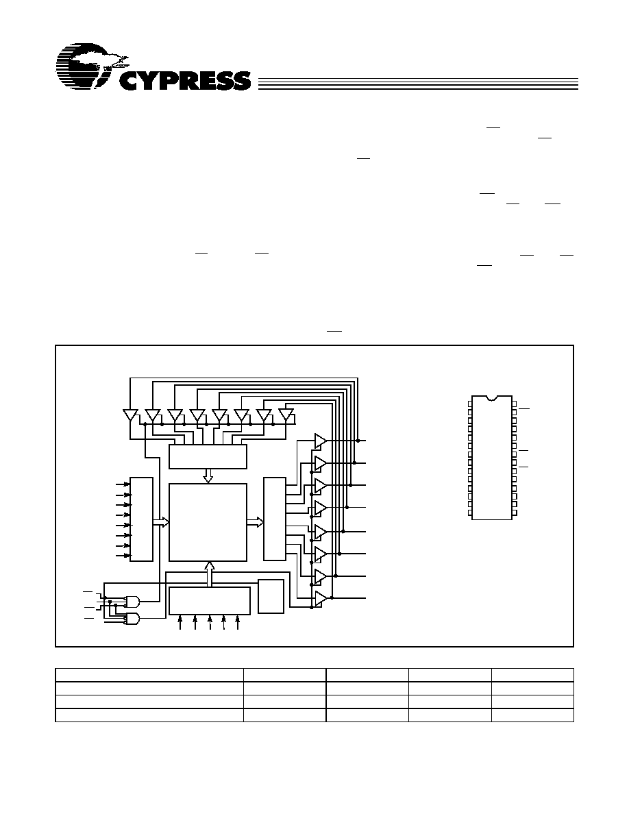
Functional Description
The CY7C185 is a high-performance CMOS static RAM orga-
nized as 8192 words by 8 bits. Easy memory expansion is
provided by an active LOW chip enable (CE
1
), an active HIGH
chip enable (CE
2
), and active LOW output enable (OE) and
three-state drivers. This device has an automatic power-down
feature (CE
1
or CE
2
), reducing the power consumption by 70%
when deselected. The CY7C185 is in a standard 300-mil-wide
DIP, SOJ, or SOIC package.
An active LOW write enable signal (WE) controls the writ-
ing/reading operation of the memory. When CE
1
and WE in-
puts are both LOW and CE
2
is HIGH, data on the eight data
input/output pins (I/O
0
through I/O
7
) is written into the memory
location addressed by the address present on the address
pins (A
0
through A
12
). Reading the device is accomplished by
selecting the device and enabling the outputs, CE
1
and OE
active LOW, CE
2
active HIGH, while WE remains inactive or
HIGH. Under these conditions, the contents of the location ad-
dressed by the information on address pins are present on the
eight data input/output pins.
The input/output pins remain in a high-impedance state unless
the chip is selected, outputs are enabled, and write enable
(WE) is HIGH. A die coat is used to insure alpha immunity.
Logic Block Diagram
Pin Configurations
C1851
A
1
A
2
A
3
A
4
A
5
A
6
A
7
A
8
A
0
A
10
A
9
A
11
A
12
I/O
0
C1852
1
2
3
4
5
6
7
8
9
10
11
12
13
14
28
27
26
25
24
23
22
21
20
19
18
17
16
15
V
CC
WE
CE
2
A
3
A
2
A
1
OE
A
0
CE
1
I/O
7
I/O
6
I/O
5
I/O
4
I/O
3
NC
A
4
A
5
A
6
A
7
A
8
A
9
A
10
A
11
A
12
I/O
0
I/O
1
I/O
2
GND
256 x 32 x 8
ARRAY
INPUT BUFFER
COLUMN DECODER
ROW
DECODER
SE
NSE A
M
P
S
POWER
DOWN
I/O
1
I/O
2
I/O
3
I/O
4
I/O
5
I/O
6
I/O
7
CE
1
CE
2
WE
OE
Top View
DIP/SOJ/SOIC
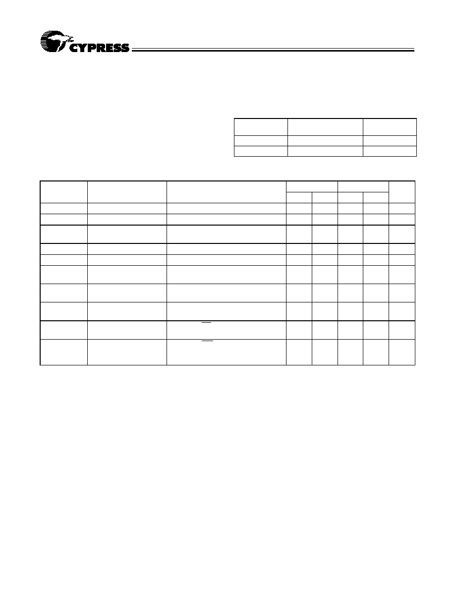
Selection Guide
[1]
7C18515
7C18520
7C18525
7C18535
Maximum Access Time (ns)
15
20
25
35
Maximum Operating Current (mA)
130
110
100
100
Maximum Standby Current (mA)
40/15
20/15
20/15
20/15
Note:
1.
For military specifications, see the CY7C185A datasheet.
CY7C185
2
Maximum Ratings
(Above which the useful life may be impaired. For user guide-
lines, not tested.)
Storage Temperature ................................. 65
°
C to +150
°
C
Ambient Temperature with
Power Applied ............................................. 55
°
C to +125
°
C
Supply Voltage to Ground Potential ............... 0.5V to +7.0V
DC Voltage Applied to Outputs
in High Z State
[2]
............................................ 0.5V to +7.0V
DC Input Voltage
[2]
......................................... 0.5V to +7.0V
Output Current into Outputs (LOW) ............................. 20 mA
Static Discharge Voltage .......................................... >2001V
(per MIL-STD-883, Method 3015)
Latch-Up Current .................................................... >200 mA
Operating Range
Range
Ambient
Temperature
V
CC
Commercial
0
°
C to +70
°
C
5V
±
10%
Industrial
40
°
C to +85
°
C
5V
±
10%
Electrical Characteristics
Over the Operating Range
7C18515
7C18520
Parameter
Description
Test Conditions
Min.
Max.
Min.
Max.
Unit
V
OH
Output HIGH Voltage
V
CC
= Min., I
OH
= 4.0 mA
2.4
2.4
V
V
OL
Output LOW Voltage
V
CC
= Min., I
OL
= 8.0 mA
0.4
0.4
V
V
IH
Input HIGH Voltage
2.2
V
CC
+
0.3V
2.2
V
CC
+
0.3V
V
V
IL
Input LOW Voltage
[2]
0.5
0.8
0.5
0.8
V
I
IX
Input Load Current
GND
V
I
V
CC
5
+5
5
+5
µ
A
I
OZ
Output Leakage
Current
GND
V
I
V
CC
,
Output Disabled
5
+5
5
+5
µ
A
I
OS
Output Short
Circuit Current
[3]
V
CC
= Max.,
V
OUT
= GND
300
300
mA
I
CC
V
CC
Operating
Supply Current
V
CC
= Max.,
I
OUT
= 0 mA
130
110
mA
I
SB1
Automatic
Power-Down Current
Max. V
CC
, CE
1
V
IH
or CE
2
V
IL
Min. Duty Cycle =100%
40
20
mA
I
SB2
Automatic
Power-Down Current
Max. V
CC
, CE
1
V
CC
0.3V,
or CE
2
0.3V
V
IN
V
CC
0.3V or V
IN
0.3V
15
15
mA
Notes:
2.
Minimum voltage is equal to 3.0V for pulse durations less than 30 ns.
3.
Not more than 1 output should be shorted at one time. Duration of the short circuit should not exceed 30 seconds.
CY7C185
3
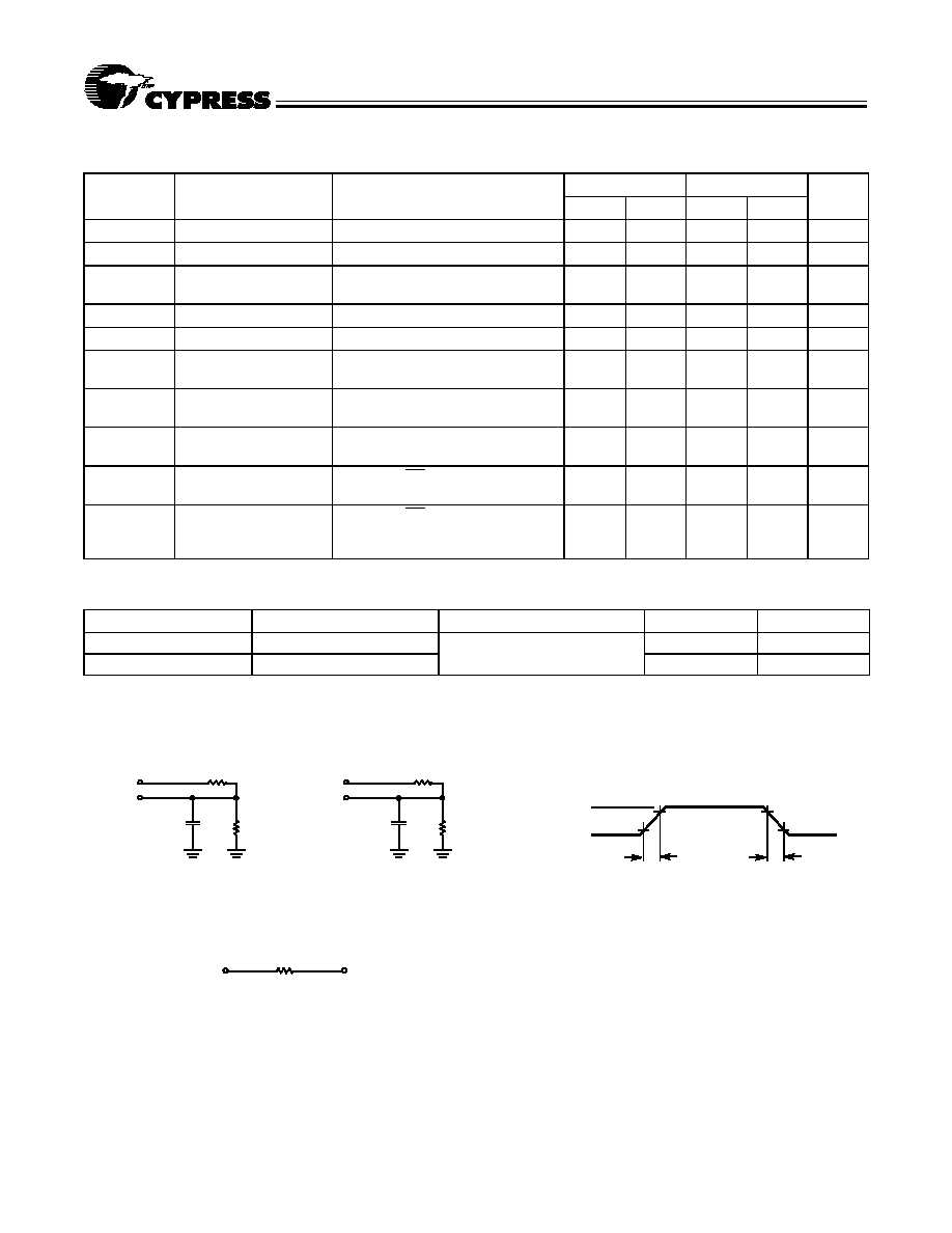
Electrical Characteristics
Over the Operating Range (continued)
7C18525
7C185-35
Parameter
Description
Test Conditions
Min.
Max.
Min.
Max.
Unit
V
OH
Output HIGH Voltage
V
CC
= Min., I
OH
= 4.0 mA
2.4
2.4
V
V
OL
Output LOW Voltage
V
CC
= Min., I
OL
= 8.0 mA
0.4
0.4
V
V
IH
Input HIGH Voltage
2.2
V
CC
+
0.3V
2.2
V
CC
+
0.3V
V
V
IL
Input LOW Voltage
[2]
0.5
0.8
0.5
0.8
V
I
IX
Input Load Current
GND
V
I
V
CC
5
+5
5
+5
µ
A
I
OZ
Output Leakage
Current
GND
V
I
V
CC
,
Output Disabled
5
+5
5
+5
µ
A
I
OS
Output Short
Circuit Current
[3]
V
CC
= Max.,
V
OUT
= GND
300
300
mA
I
CC
V
CC
Operating
Supply Current
V
CC
= Max.,
I
OUT
= 0 mA
100
100
mA
I
SB1
Automatic
Power-Down Current
Max. V
CC
, CE
1
V
IH
or
CE
2
V
IL
Min. Duty Cycle =100%
20
20
mA
I
SB2
Automatic
Power-Down Current
Max. V
CC
, CE
1
V
CC
0.3V
or CE
2
0.3V
V
IN
V
CC
0.3V or V
IN
0.3V
15
15
mA
Capacitance
[4]
Parameter
Description
Test Conditions
Max.
Unit
C
IN
Input Capacitance
T
A
= 25
°
C, f = 1 MHz,
V
CC
= 5.0V
7
pF
C
OUT
Output Capacitance
7
pF
Note:
4.
Tested initially and after any design or process changes that may affect these parameters.
AC Test Loads and Waveforms
R1 481
3.0V
5V
OUTPUT
R1 481
R2
255
30 pF
GND
90%
90%
10%
5 ns
5 ns
5V
OUTPUT
C1854
R2
255
5 pF
C1855
(a)
(b)
OUTPUT
1.73V
INCLUDING
JIG AND
SCOPE
INCLUDING
JIGAND
SCOPE
10%
Equivalent to:
THÉVENIN EQUIVALENT
ALL INPUT PULSES
167
CY7C185
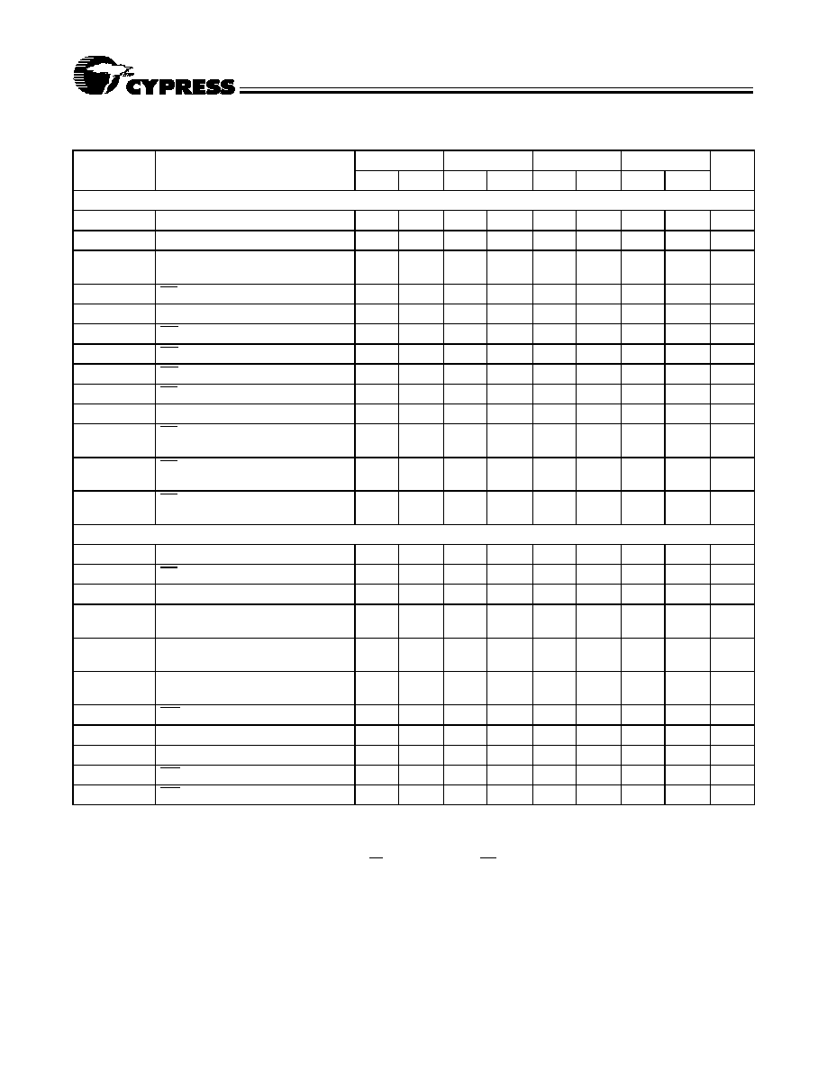
4
Switching Characteristics
Over the Operating Range
[5]
7C18515
7C18520
7C18525
7C18535
Parameter
Description
Min.
Max.
Min.
Max.
Min.
Max.
Min.
Max.
Unit
READ CYCLE
t
RC
Read Cycle Time
15
20
25
35
ns
t
AA
Address to Data Valid
15
20
25
35
ns
t
OHA
Data Hold from
Address Change
3
5
5
5
ns
t
ACE1
CE
1
LOW to Data Valid
15
20
25
35
ns
t
ACE2
CE
2
HIGH to Data Valid
15
20
25
35
ns
t
DOE
OE LOW to Data Valid
8
9
12
15
ns
t
LZOE
OE LOW to Low Z
3
3
3
3
ns
t
HZOE
OE HIGH to High Z
[6]
7
8
10
10
ns
t
LZCE1
CE
1
LOW to Low Z
[7]
3
5
5
5
ns
t
LZCE2
CE
2
HIGH to Low Z
3
3
3
3
ns
t
HZCE
CE
1
HIGH to High Z
[6, 7]
CE
2
LOW to High Z
7
8
10
10
ns
t
PU
CE
1
LOW to Power-Up
CE
2
to HIGH to Power-Up
0
0
0
0
ns
t
PD
CE
1
HIGH to Power-Down
CE
2
LOW to Power-Down
15
20
20
20
ns
WRITE CYCLE
[8]
t
WC
Write Cycle Time
15
20
25
35
ns
t
SCE1
CE
1
LOW to Write End
12
15
20
20
ns
t
SCE2
CE
2
HIGH to Write End
12
15
20
20
ns
t
AW
Address Set-Up to
Write End
12
15
20
25
ns
t
HA
Address Hold from
Write End
0
0
0
0
ns
t
SA
Address Set-Up to
Write Start
0
0
0
0
ns
t
PWE
WE Pulse Width
12
15
15
20
ns
t
SD
Data Set-Up to Write End
8
10
10
12
ns
t
HD
Data Hold from Write End
0
0
0
0
ns
t
HZWE
WE LOW to High Z
[6]
7
7
7
8
ns
t
LZWE
WE HIGH to Low Z
3
5
5
5
ns
Notes:
5.
Test conditions assume signal transition time of 5 ns or less, timing reference levels of 1.5V, input pulse levels of 0 to 3.0V, and output loading of the specified
I
OL
/I
OH
and 30-pF load capacitance.
6.
t
HZOE,
t
HZCE
, and t
HZWE
are specified with C
L
= 5 pF as in part (b) of AC Test Loads. Transition is measured
±
500 mV from steady state voltage.
7.
At any given temperature and voltage condition, t
HZCE
is less than t
LZCE1
and t
LZCE2
for any given device.
8.
The internal write time of the memory is defined by the overlap of CE
1
LOW, CE
2
HIGH, and WE LOW. All 3 signals must be active to initiate a write and either
signal can terminate a write by going HIGH. The data input set-up and hold timing should be referenced to the rising edge of the signal that terminates the write.
CY7C185
5
Switching Waveforms
9.
Device is continuously selected. OE, CE
1
= V
IL
. CE
2
= V
IH
.
10. WE is HIGH for read cycle.
11. Data I/O is High Z if OE = V
IH
, CE
1
= V
IH
, WE = V
IL
,
or CE
2
=V
IL
.
12. The internal write time of the memory is defined by the overlap of CE
1
LOW, CE
2
HIGH and WE LOW. CE
1
and WE must be LOW and CE
2
must be HIGH
to initiate write. A write can be terminated by CE
1
or WE going HIGH or CE
2
going LOW. The data input set-up and hold timing should be referenced to the
rising edge of the signal that terminates the write.
13. During this period, the I/Os are in the output state and input signals should not be applied.
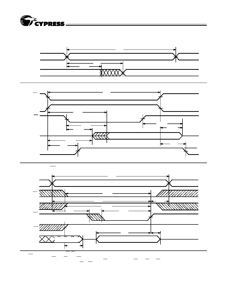
ADDRESS
DATA OUT
PREVIOUS DATA VALID
DATA VALID
t
RC
t
AA
t
OHA
C1856
Read Cycle No.1
[9,10]
50%
50%
DATA VALID
t
RC
t
ACE
t
DOE
t
LZOE
t
LZCE
t
PU
HIGH IMPEDANCE
IMPEDANCE
ICC
ISB
t
HZOE
t
HZCE
t
PD
OE
HIGH
DATA OUT
V
CC
SUPPLY
CURRENT
CE
1
OE
CE
2
C1857
Read Cycle No.2
[11,12]
C1858
t
HD
t
SD
t
PWE
t
SA
t
HA
t
AW
t
WC
t
HZOE
DATA
IN
VALID
CE
CE
1
OE
WE
CE
2
DATA I/O
t
SCEI
t
SCE2
ADDRESS
NOTE 13
[10,12]
Write Cycle No. 1 (WE Controlled)
CY7C185
6
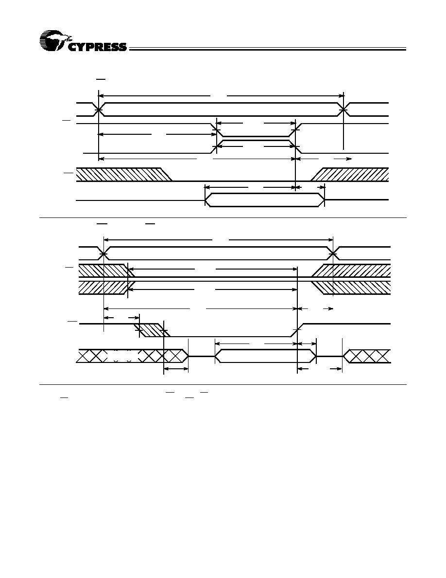
Notes:
14. The minimum write cycle time for write cycle #3 (WE controlled, OE LOW) is the sum of t
HZWE
and t
SD
.
15. If CE
1
goes HIGH or CE
2
goes LOW simultaneously with WE HIGH, the output remains in a high-impedance state.
Switching Waveforms
(continued)
t
WC
t
AW
t
SA
t
HA
t
HD
t
SD
t
SCE1
WE
DATA I/O
ADDRESS
CE
1
C1859
DATA
IN
VALID
t
SCE2
CE
2
Write Cycle No. 2 (CE Controlled)
[12,13,14]
t
HD
t
SD
t
LZWE
t
SA
t
HA
t
AW
t
WC
t
HZWE
C18510
DATA
IN
VALID
t
SCE1
t
SCE2
CE
1
CE
2
ADDRESS
DATA I/O
WE
Write Cycle No. 3 (WE Controlled, OE LOW)
[12,13,14,15]
NOTE 13
CY7C185
7
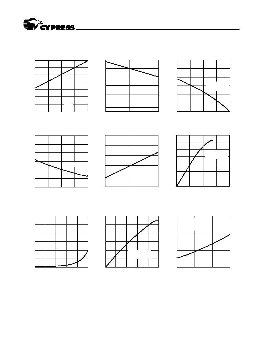
Typical DC and AC Characteristics
55
25
125
1.2
1.0
0.8
O
U
T
P
UT
SOURCE
CURRENT
(m
A)
AMBIENT TEMPERATURE (
°
C)
0.6
0.4
0.2
0.0
N
O
R
M
A
L
IZ
ED
I
, I
CC
I
SB
V
CC
=5.0V
V
IN
=5.0V
I
CC
SB
1.2
1.4
1.0
0.6
0.4
0.2
4.0
4.5
5.0
5.5
6.0
1.6
1.4
1.2
1.0
0.8
55
25
125
N
O
RM
AL
IZ
ED t
AA
120
100
80
60
40
20
0.0
1.0
2.0
3.0
4.0
SUPPLY VOLTAGE (V)
NORMALIZED SUPPLY CURRENT
vs. SUPPLY VOLTAGE
NORMALIZED ACCESS TIME
vs. AMBIENT TEMPERATURE
AMBIENT TEMPERATURE (
°
C)
NORMALIZED SUPPLY CURRENT
vs. AMBIENT TEMPERATURE
OUTPUT VOLTAGE (V)
OUTPUT SOURCE CURRENT
vs. OUTPUT VOLTAGE
0.0
0.8
1.4
1.3
1.2
1.1
1.0
0.9
4.0
4.5
5.0
5.5
6.0
N
O
R
M
AL
IZ
ED t
AA
SUPPLY VOLTAGE (V)
NORMALIZED ACCESS TIME
vs. SUPPLY VOLTAGE
120
140
100
60
40
20
0.0
1.0
2.0
3.0
4.0
OUT
P
UT
SI
NK CURRENT
(m
A)
0
80
OUTPUT VOLTAGE (V)
OUTPUT SINK CURRENT
vs. OUTPUT VOLTAGE
N
O
R
M
A
L
IZ
ED
I
, I
CC
S
B
I
CC
V
CC
=5.0V
V
CC
=5.0V
T
A
=25
°
C
V
CC
=5.0V
T
A
=25
°
C
I
SB
T
A
=25
°
C
0.6
0.8
0
3.0
2.5
2.0
1.5
1.0
0.5
0.0
1.0
2.0
3.0
4.0
NORM
A
L
I
Z
ED I
PO
SUPPLY VOLTAGE (V)
TYPICAL POWER-ON CURRENT
vs. SUPPLY VOLTAGE
30.0
25.0
20.0
15.0
10.0
5.0
0
200
400
600
800
D
E
L
T
A t
(n
s
)
AA
CAPACITANCE (pF)
TYPICAL ACCESS TIME CHANGE
vs. OUTPUT LOADING
1.25
1.00
0.75
10
20
30
40
NORM
A
L
I
Z
ED I
CC
CYCLE FREQUENCY (MHz)
NORMALIZED I
CC
vs. CYCLE TIME
0.0
5.0
0.0
1000
0.50
V
CC
=4.5V
T
A
=25
°
C
V
CC
=5.0V
T
A
=25
°
C
V
CC
=0.5V
CY7C185
8
Document #: 3800037K
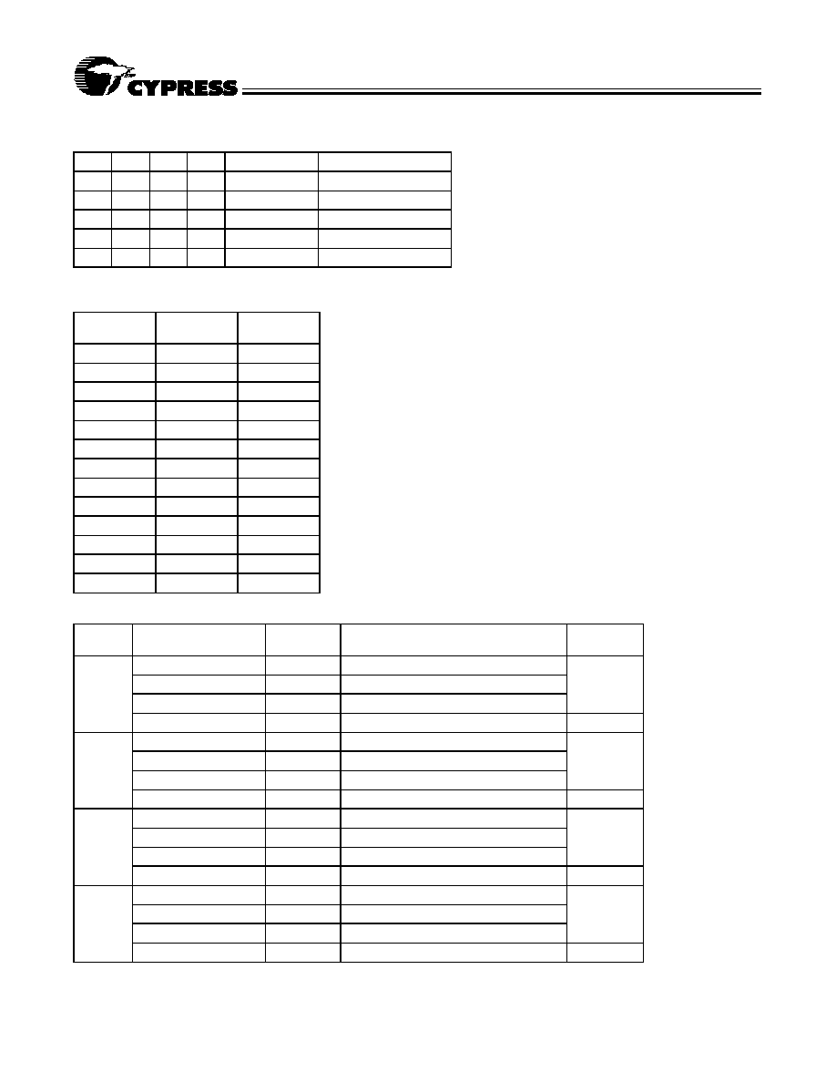
Truth Table
CE
1
CE
2
WE
OE
Input/Output
Mode
H
X
X
X
High Z
Deselect/Power-Down
X
L
X
X
High Z
Deselect/Power-Down
L
H
H
L
Data Out
Read
L
H
L
X
Data In
Write
L
H
H
H
High Z
Deselect
Address Designators
Address
Name
Address
Function
Pin
Number
A4
X3
2
A5
X4
3
A6
X5
4
A7
X6
5
A8
X7
6
A9
Y1
7
A10
Y4
8
A11
Y3
9
A12
Y0
10
A0
Y2
21
A1
X0
23
A2
X1
24
A3
X2
25
Ordering Information
Speed
(ns)
Ordering Code
Package
Name
Package Type
Operating
Range
15
CY7C18515PC
P21
28-Lead (300-Mil) Molded DIP
Commercial
CY7C18515SC
S21
28-Lead Molded SOIC
CY7C18515VC
V21
28-Lead Molded SOJ
CY7C18515VI
V21
28-Lead Molded SOJ
Industrial
20
CY7C18520PC
P21
28-Lead (300-Mil) Molded DIP
Commercial
CY7C18520SC
S21
28-Lead Molded SOIC
CY7C18520VC
V21
28-Lead Molded SOJ
CY7C18520VI
V21
28-Lead Molded SOJ
Industrial
25
CY7C18525PC
P21
28-Lead (300-Mil) Molded DIP
Commercial
CY7C18525SC
S21
28-Lead Molded SOIC
CY7C18525VC
V21
28-Lead Molded SOJ
CY7C18525VI
V21
28-Lead Molded SOJ
Industrial
35
CY7C18535PC
P21
28-Lead (300-Mil) Molded DIP
Commercial
CY7C18535SC
S21
28-Lead Molded SOIC
CY7C18535VC
V21
28-Lead Molded SOJ
CY7C18535VI
V21
28-Lead Molded SOJ
Industrial
CY7C185
9
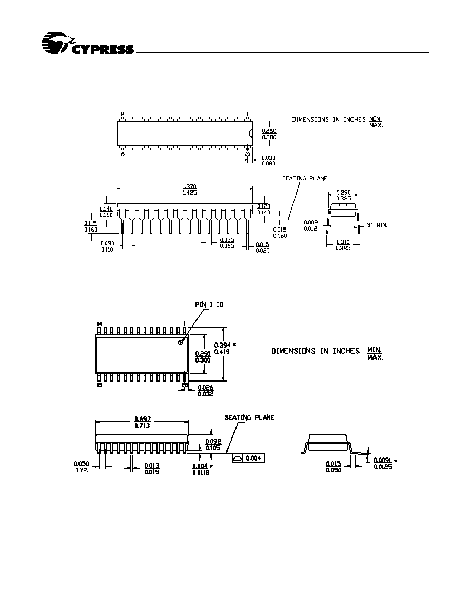
Package Diagrams
51-85014-B
28-Lead (300-Mil) Molded DIP P21
28-Lead (300-Mil) Molded SOIC S21
51-85026-A
CY7C185
© Cypress Semiconductor Corporation, 1998. The information contained herein is subject to change without notice. Cypress Semiconductor Corporation assumes no responsibility for the use
of any circuitry other than circuitry embodied in a Cypress Semiconductor product. Nor does it convey or imply any license under patent or other rights. Cypress Semiconductor does not authorize
its products for use as critical components in life-support systems where a malfunction or failure may reasonably be expected to result in significant injury to the user. The inclusion of Cypress
Semiconductor products in life-support systems application implies that the manufacturer assumes all risk of such use and in doing so indemnifies Cypress Semiconductor against all charges.
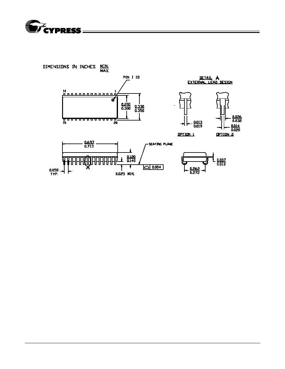
Package Diagrams
(continued)
28-Lead (300-Mil) Molded SOJ V21
51-85031-B