 | ÐлекÑÑоннÑй компоненÑ: CY2PP3115 | СкаÑаÑÑ:  PDF PDF  ZIP ZIP |
38-07502.fm
PRELIMINARY
1:15 Differential Fanout Buffer
FastEdgeTM Series
CY2PP3115
Cypress Semiconductor Corporation
·
3901 North First Street
·
San Jose
,
CA 95134
·
408-943-2600
Document #: 38-07502 Rev.*A
Revised November 18, 2003
Features
· Fifteen ECL/PECL differential outputs grouped in four
banks
· Two ECL/PECLdifferential inputs
· Hot-swappable/-insertable
· 50-ps output-to-output skew
· < 200-ps device-to-device skew
· Less than 2-pS intrinsic jitter
· < 500-ps propagation delay (typical)
· Operation up to 1.5 GHz
· PECL mode supply range: V
CC
= 2.375V to 3.465V with
V
EE
= 0V
· ECL mode supply range: V
EE
= 2.375V to 3.465V with
V
CC
= 0V
· Industrial temperature range: 40
°
C to 85
°
C
· 52-pin 1.4mm TQFP package
· Temperature compensation like 100K ECL
Description
The CY2PP3115 is a low-skew, low propagation delay 1-to-15
differential fanout buffer targeted to meet the requirements of
high-performance clock and data distribution applications. The
device is implemented on SiGe technology and has a fully
differential internal architecture that is optimized to achieve
low-signal skews at operating frequencies of up to 1.5 GHz.
The device features two differential input paths which are
multiplexed internally. This mux is controlled by the CLK_SEL
pin. The CY2PP3115 may function not only as a differential
clock buffer but also as a signal level translator and fanout on
ECL/PECL single-ended signal to 15 ECL/PECL differential
loads. An external bias pin, VBB, is provided for this purpose.
In such an application, the VBB pin should be connected to
either one of the CLKA# or CLKB# inputs and bypassed to V
CC
via a 0.01-
µF capacitor.
Since the CY2PP3115 introduces negligible jitter to the timing
budget, it is the ideal choice for distributing high frequency,
high precision clocks across back-planes and boards in
communication systems. Furthermore, advanced circuit
design schemes, such as internal temperature compensation,
ensure that the CY2PP3115 delivers consistent, guaranteed
performance over differing platforms.
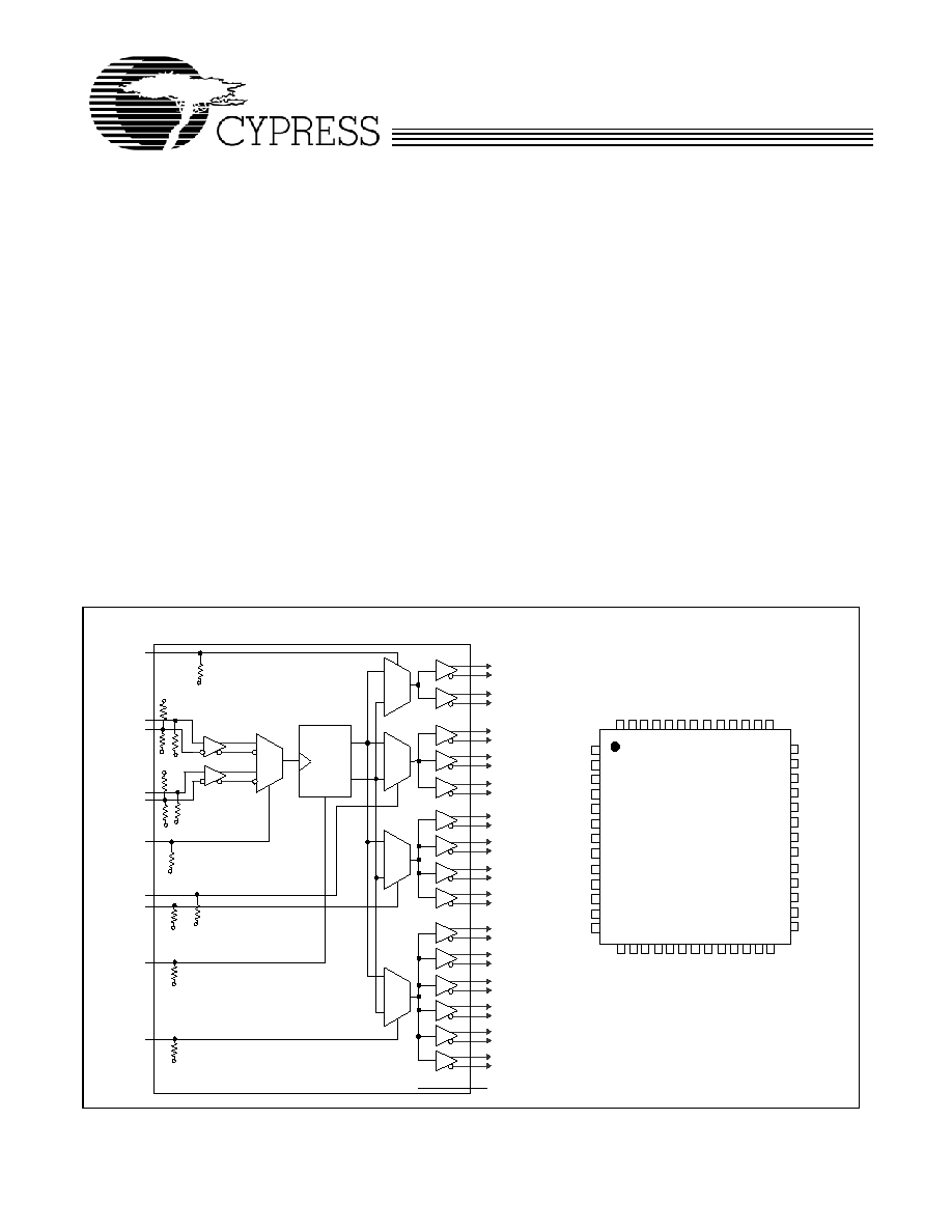
Block Diagram
Pin Configuration
CY2PP3115
1
2
3
4
5
6
7
8
9
10
11
12
13
14
15
16
17
18
19
20
21
22
23
24
25
26
52
51
50
49
48
47
46
45
44
43
42
41
40
39
38
37
36
35
34
33
32
31
30
29
28
27
VCC
QC0
QC0#
QC1
QC1#
QC2
QC2#
QC3
QC3#
VCC
NC
NC
VCC
V
C
C
Q
A
0
Q
A
0
#
Q
A
1
Q
A
1
#
V
C
C
Q
B
0
Q
B
0
#
Q
B
1
Q
B
1
#
Q
B
2
Q
B
2
#
V
C
C
VCC
MR
FSELA
FSELB
CLK0
CLK0#
CLK_SEL
CLK1
CLK1#
VBB
FSELC
FSELD
VEE
VCC
QD5#
QD5
QD4#
QD4
QD3#
QD3
QD2#
QD2
QD1#
QD1
QD0#
QD0
0
1
0
1
1
0
0
1
QAO
QA1
QBO
QB1
QB2
QC0
QC1
QC2
QC3
QD0
QD1
QD2
QD3
QD4
QD5
VBB
VEE
VEE
VEE
VEE
VEE
VEE
VEE
VCC
VCC
0
1
/1
/2
FSELA
CLK0
CLK0#
CLK1
CLK1#
FSELB
FSELC
MR
FSELD
CLK_SEL
PRELIMINARY
FastEdgeTM Series
CY2PP3115
Document #: 38-07502 Rev.*A
Page 2 of 12
Governing Agencies
The following agencies provide specifications that apply to the
CY2PP3115. The agency name and relevant specification is
listed below.
Pin Description
Pin No.
Name
[2,3]
I/O
[1]
Type
Description
1,14,27, 30, 39, 40, 47,
52
VCC
+PWR POWER
Power Supply, positive connection
2
MR
I,PD
ECL/PECL
Reset
3,4,11,12
FSEL(A,B,C,D)
I,PD
ECL/PECL
Output Divider Selects
5,8
CLK(0:1)
I,PD
ECL/PECL
Differential Clock Inputs TRUE
6,9
CLK(0:1)#
I,PC
ECL/PECL
Differential Clock Inputs COMPLIMENT
10
VBB
O
Bias
DC Bias Source
13
VEE
PWR
POWER
Power Supply, Negative Connection
28,29
NC
No Connect. Pad Only
7
CLK_SEL
I,PD
ECL/PECL
Clock Input Select
26,24,22,20,18,16
QD(0:5)
O,OE
ECL/PECL
Bank D True Output
25,23,21,19,17,15
QD(0:5)#
O,OE
ECL/PECL
Bank D Compliment Output
38,36,34,32
QC(0:3)
O,OE
ECL/PECL
Bank C True Output
37,35,33,31
QC(0:3)#
O,OE
ECL/PECL
Bank C Compliment Output
46,44,42
QB(0:2)
O,OE
ECL/PECL
Bank B True Output
45,43,41
QB(0:2)#
O,OE
ECL/PECL
Bank B Compliment Output
51,49
QA(0:1)
O,OE
ECL/PECL
Bank A True Output
50,48
QA(0:1)#
O,OE
ECL/PECL
Bank A Compliment Output
Table 1. Function Table
Control Pin
0
1
FSELA (Asynchronous)
÷1
÷2
FSELB (Asynchronous)
÷1
÷2
FSELC (Asynchronous)
÷1
÷2
FSELD (Asynchronous)
÷1
÷2
CLK_SEL (Asynchronous)
CLK0
CLK1
MR (Asynchronous)
Active
Reset (QX = L and QX# = H)
Agency Name
Specification
JEDEC
JESD 51 (Theta JA)
JESD 82 (ECL)
JESD 65A (skew,jitter)
IEEE
1596.3 (Jitter specs)
UL
94 (Flammability Grading)
MilSpec
883E Method 1012.1
(Thermal Theta JC)
Notes:
1.
In the I/O column, the following notation is used: I for Input, O for Output, PD for Pull-down, PU for Pull-up, PC for Pull Center, O for output, OE for open emitter
and PWR for Power.
2.
In ECL mode (negative power supply mode), V
EE
is either 3.3V or 2.5V and V
CC
is connected to GND (0V). In PECL mode (positive power supply mode),
V
EE
is connected to GND (0V) and V
CC
is either +3.3V or +2.5V. In both modes, the input and output levels are referenced to the most positive supply (V
CC
)
and are between VCC and VEE.
3.
V
BB
is available for use for single ended bias mode when V
CC
is +3.3V.
PRELIMINARY
FastEdgeTM Series
CY2PP3115
Document #: 38-07502 Rev.*A
Page 3 of 12
.
Absolute Maximum Conditions
Parameter
Description
Condition
Min.
Max.
Unit
V
CC
Supply Voltage
Non-Functional
0.3
4.6
VDC
V
CC
Operating Voltage
Functional
2.5 5%
3.3 + 5%
VDC
V
BB
Output Reference Voltage
Relative to V
CC
V
CC
1.620
Vcc1.220
VDC
I
BB
Output Reference Current
Relative to V
BB
200
uA
VTT
Output Termination Voltage
Relative to V
CC
V
CC
2
VDC
V
IN
Input Voltage
Relative to V
CC
0.3
V
CC
+0.3
VDC
V
OUT
Output Voltage
Relative to V
CC
0.3
V
CC
+0.3
VDC
LU
I
Latch-up Immunity
Functional
300
mA
T
S
Temperature, Storage
Non-functional
65
+150
°C
T
A
Temperature, Operating Ambient
Functional
40
+85
°C
Ø
Jc
Dissipation, Junction to Case
Functional
40
60
°C/W
Ø
Ja
Dissipation, Junction to Ambient
Functional
40
100
°C/W
ESD
h
ESD Protection (Human Body Model)
2000
V
M
SL
Moisture Sensitivity Level
3
N.A.
G
ATES
Total Functional Gate Count
Assembled Die
50
Ea.
ULFLM
Flammability Rating
@ 1/8 in.
V0
N.A.
PECL DC Electrical Specifications
Parameter
Description
Condition
Min.
Max.
Unit
Control (FSEL(A,B,C),CLK_SEL, MR and FSELD) (PECL Single-ended)
V
CC2.5V
2.5 Operating Voltage
2.5V ± 5%, V
EE
= 0.0V
2.375
2.625
V
V
CC3.3V
3.3 Operating Voltage
3.3V ± 5%, V
EE
= 0.0V
3.135
3.465
V
V
IL
Input Voltage, Low
V
CC
1.945
V
CC
1.625
V
V
IH
Input Voltage, High
V
CC
1.165
V
CC
0.880
V
I
IN
Input Current
[4]
V
IL
= V
IL
min. or V
IH
= V
IH
max
at V
CC
= 3.6V
I150I
uA
Clock input pair CLK0, CLK0#,CLK1,CLK1# (PECL Differential Signals)
V
PP
Differential input voltage
[5]
Differential operation
0.1
1.3
V
V
CMR
Differential cross point voltage
[6]
Differential operation
1.2
V
CC
V
I
IN
Input Current
[4]
V
IL
= V
IL
min. or V
IH
= V
IH
max
at V
CC
= 3.6V
I150I
uA
PECL Outputs QA((0:1),#),QB((0:2),#),QC((0:3),#),QD((0:5),#)(PECL Differential Signals)
V
OH
Output High Voltage
I
OH
= 30 mA
[7]
V
CC
1.2
V
CC
0.7
V
V
OL
Output Low Voltage
V
CC
= 3.3V ± 5%, V
CC
= 2.5V ± 5%
I
OL
= 5 ma
[7]
V
CC
1.945
V
CC
1.945
V
CC
1.5
V
CC
1.3
V
Supply Current and VBB
I
EE
Maximum Quiescent Supply Current
without output termination current
[8]
V
EE
pin
200
mA
V
BB
[9]
Output reference voltage
I
BB
= 200 uA
[12]
V
CC
1.620
V
CC
1.220
V
C
IN
Input pin capacitance
2.0
pF
L
IN
Pin Inductance
1.0
nH
Notes:
4.
Input have internal pull-up/pull-down or biasing resistors which affect the input current.
5.
VPP (DC) is the minimum differential input voltage swing required to maintain device functionality.
6.
VCMR (DC) is the crosspoint of the differential input signal. Functional operation is obtained when the crosspoint is within the VCMR (DC) range and the input
swing lies within the VPP (DC) specification.
7.
Equivalent to a termination of 50
to VTT.
8.
ICC Calculation: ICC = (number of differential output pairs used) x (I
OH
+ I
OL
) + I
EE
orI
CC
= (number of differential output pairs used) x (V
OH
VTT)/Rload +
(V
OL
-VTT)/Rload +IEE.
9.
VBB is limited to VCC of 3.3V only. See note 17.
PRELIMINARY
FastEdgeTM Series
CY2PP3115
Document #: 38-07502 Rev.*A
Page 4 of 12
ECL DC Electrical Specifications
Parameter
Description
Condition
Min.
Max.
Unit
Control (FSEL(A,B,C),CLK_SEL, MR and FSELD) (ECL single-ended)
V
EE2.5
2.5 Negative Power Supply
2.5V ± 5%, V
EE
= 0.0V
2.375
2.625
V
V
EE3.3
3.3 Negative Power Supply
3.3V ± 5%, V
EE
= 0.0V
33.135
3.465
V
V
IL
Input Voltage, Low
1.945
1.625
V
V
IH
Input Voltage, High
1.165
0.880
V
I
IN
Input Current
[10]
V
IN
= V
IL
or V
IN
= V
IH
I150I
uA
Clock input pair CLK0, CLK0#,CLK1,CLK1# (ECL differential signals)
V
PP
Differential input voltage
[11]
Differential operation
0.1
1.3
V
V
CMR
Differential cross point voltage
[12]
Differential operation
V
EE
+1.2
0.5
V
I
IN
Input Current
[10]
V
IN
= V
IL
or V
IN
= V
IH
I150I
uA
ECL Outputs QA((0:1),#),QB((0:2),#),QC((0:3),#),QD((0:5),#)(ECL differential signals)
V
OH
Output High Voltage
I
OH
= 30 mA
[13]
1.2
0.7
V
V
OL
Output Low Voltage
V
EE
= 3.3V ± 5%,V
EE
= 2.5V ± 5%
I
OL
= 5 ma
[13]
1.945
1.945
1.5
1.3
V
Supply current and VBB
I
EE
Maximum Quiescent Supply Current
without output termination current
[14]
V
EE
pin
180
mA
V
BB
Output reference voltage
I
BB
= 200 uA
1.620
1.220
V
AC Electrical Specifications
Parameter
Description
Condition
Min.
Max. Unit
Clock input pair CLK0, CLK0#,CLK1,CLK1#(PECL or ECL differential signals)
V
PP
Differential input voltage
[16]
Differential operation
0.1
1.3
V
V
CMR
Differential cross point voltage
[17]
Differential operation
V
EE
+ 1.2
0
V
F
CLK
Input Frequency
[18]
50% duty cycle Standard load
1500 MHz
T
PD
Propagation Delay CLK0 or CLK1 to
QA(0:1),QB(0:2),QC(0:3),QD(0:5) pair
660 MHz 50% duty cycle Standard load Differ-
ential Operation. See Table 2
600
1200
ps
ECL/PECL Clock Outputs QA((0:1),#),QB((0:2),#),QC((0:3),#),QD((0:5),#) (differential)
Vo
(P-P)
Differential output voltage
(peak-to-peak)
Differential PRBS
fo < 50 MHz
fo < 0.8 GHz
fo < 1.0 GHz
fo < 1.5 GHz
0.45
0.4
0.375
0.3
V
VMCR
Common Voltage Range
V
CC
1.425
ps
tsk
(O)
Output-to-output skew
660 MHz 50% duty cycle Standard load Differ-
ential Operation
50
ps
tsk
(O)
Output-to-output skew (different
frequency)
660 MHz 50% duty cycle Standard load Differ-
ential Operation
60
ps
Notes:
10. Input have internal pullup / pulldown or biasing resistors which affect the input current.
11. VPP (DC) is the minimum differential input voltage swing required to maintain device functionality.
12. VCMR (DC) is the crosspoint of the differential input signal. Functional operation is obtained when the crosspoint is within the VCMR (DC) range and the input
swing lies within the VPP (DC) specification.
13. Equivalent to a termination of 50
to VTT.
14. I
CC
Calculation: ICC = (number of differential output pairs used) x (I
OH
+ I
OL
) + IEE or I
CC
= (number of differential output pairs used) x (V
OH
VTT)/Rload +
(V
OL
VTT)/Rload +I
EE
.
15. AC characteristics apply for parallel output termination of 50
to VTT.
16. VPP (AC) is the minimum differential ECL/PECL input swing required to maintain AC characteristics including tpd and device-to-device skew.
17. VCMR (AC) is the crosspoint of the differential ECL/PECL input signal. Normal AC operation is obtained when the crosspoint is within the VCMR(AC) range and
the input swing lies within the VPP(AC) specification. Violation of VCMR(AC) or VPP(AC) impacts the device propagation delay, device and part-to-part skew.
18. The CY2PP3115 is fully operation up to 1.5 GHz.
PRELIMINARY
FastEdgeTM Series
CY2PP3115
Document #: 38-07502 Rev.*A
Page 5 of 12
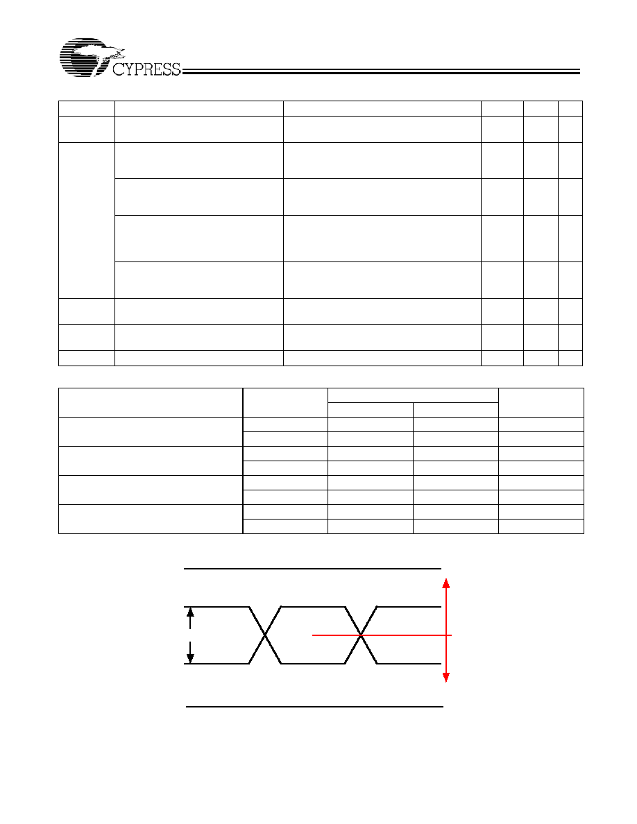
Timing Definitions
Note:
19. Output pulse skew is the absolute difference of the propagation delay times: | tPLH tPHL |.
tsk
(PP)
Output-to-output skew (part-to-part)
50% duty cycle Standard load Differential
Operation
200
ps
T
JIT(CC)
Output cycle-to-cycle jitter (determin-
istic/Intrinsic)
All outputs /1
500 MHz 50% duty cycle Standard load Differ-
ential Operation
2
ps
Output cycle-to-cycle jitter (determin-
istic/Intrinsic)
All outputs /2
660 MHz 50% duty cycle Standard load Differ-
ential Operation
2
ps
Output cycle-to-cycle jitter (determin-
istic/Intrinsic)
All outputs Bank(A and C)/1, Bank(B and
D)/2
660 MHz 50% duty cycle Standard load Differ-
ential Operation
2
ps
Output cycle-to-cycle jitter (determin-
istic/Intrinsic)
All outputs Bank A/1, Bank(B,C and D)/2
660 MHz 50% duty cycle Standard load Differ-
ential Operation
2
ps
tsk
(P)
Output pulse skew
[19]
660 MHz 50% duty cycle Standard load Differ-
ential Operation
75
ps
T
R
,T
F
Output Rise / Fall time
660 MHz 50% duty cycle Differential 20% to
80%
0.3
ns
TTB
Total Timing Budget
500 MHz 50% duty cycle Standard load
250
ps
Table 2. TPDPropagation Delay 66-MHz 50% Duty Cycle
TPD
CLK_SEL
Unit
0
1
FSELA
0
0.900
0.974
ns
1
0.979
0.982
ns
FSELB
0
0.951
0.974
ns
1
0.962
0.966
ns
FSELC
0
0.952
0.974
ns
1
1.019
1.021
ns
FSELD
0
0.986
0.980
ns
1
1.018
1.022
ns
AC Electrical Specifications
Parameter
Description
Condition
Min.
Max. Unit
VIH
VIL
VCMR
VPP
VCMR Min = 1.2V
VPP range
0.1V - 1.3V
VCMR Max = VCC
VCC = 2.5V or 3.3V
VCC
VEE
VEE = 0.0V
Figure 1. PECL Waveform Definitions