 | –≠–ª–µ–∫—Ç—Ä–æ–Ω–Ω—ã–π –∫–æ–º–ø–æ–Ω–µ–Ω—Ç: CY2DP314 | –°–∫–∞—á–∞—Ç—å:  PDF PDF  ZIP ZIP |

1 of 2:4 Differential Clock/Data Fanout Buffer
CY2DP314
Cypress Semiconductor Corporation
∑
3901 North First Street
∑
San Jose
,
CA 95134
∑
408-943-2600
Document #: 38-07550 Rev.*E
Revised September 27, 2004
Features
∑ Four ECL/PECL differential outputs
∑ One ECL/PECL differential or single-ended inputs
(CLKA)
∑ One HSTL differential or single-ended inputs (CLKB)
∑ Hot-swappable/-insertable
∑ 50-ps output-to-output skew
∑ 150-ps device-to-device skew
∑ 400-ps propagation delay (typical)
∑ 0.8-ps RMS period jitter (max.)
∑ 1.5-GHz operation (2.7-GHz maximum toggle
frequency)
∑ PECL and HSTL mode supply range: V
CC
= 2.5V± 5% to
3.3V±5% with V
EE
= 0V
∑ ECL mode supply range: V
E E
= ≠2.5V± 5% to ≠3.3V±5%
with V
CC
= 0V
∑ Industrial temperature range: ≠40∞C to 85∞C
∑ 20-pin SSOP package
∑ Temperature compensation like 100K ECL
Functional Description
The CY2DP314 is a low-skew, low propagation delay 2-to-4
differential fanout buffer targeted to meet the requirements of
high-performance clock and data distribution applications. The
device is implemented on SiGe technology and has a fully
differential internal architecture that is optimized to achieve
low signal skews at operating frequencies of up to 1.5 GHz (full
swing).
The device features two differential input paths that are multi-
plexed internally. This mux is controlled by the CLK_SEL pin.
The CY2DP314 may function not only as a differential clock
buffer but also as a signal-level translator and fanout on HSTL
or LVCMOS /LVTTL single-ended signal to four ECL/PECL
differential loads.
Since the CY2DP314 introduces negligible jitter to the timing
budget, it is the ideal choice for distributing high frequency,
high precision clocks across back-planes and boards in
communication systems. Furthermore, advanced circuit
design schemes, such as internal temperature compensation,
ensure that the CY2DP314 delivers consistent performance
over various platforms.
Block Diagram
Pin Configuration
20
19
18
17
16
15
14
13
12
11
1
2
3
4
5
6
7
8
9
10
CY2DP314
20 pin SSOP
VCC
Q0
Q0#
Q1
Q1#
Q2
Q2#
Q3
Q3#
VCC
VCC
NC
VCC
CLK_SEL
CLKA
CLKA#
CLKB
CLKB#
VEE
VCC
Q0
Q0#
Q1
Q1#
Q2
Q2#
Q3
Q3#
VEE
VEE
VCC
CLKA
CLKA#
CLKB
CLKB#
CLK_SEL
VEE
VCC
CY2DP314
Document #: 38-07550 Rev.*E
Page 2 of 9
Governing Agencies
The following agencies provide specifications that apply to the
CY2DP314. The agency name and relevant specification is
listed below in Table 2.
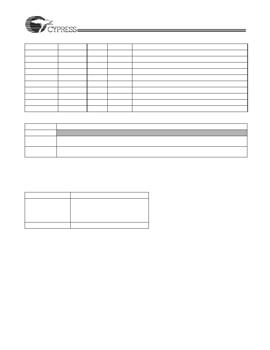
Pin Definitions
Pin
Name
I/O
Type
Description
1,10,11,20,3
VCC
+PWR
Power
Power supply, positive connection
2
NC
No connect
4
CLK_SEL
I,PD
LVCMOS
InPut Clock Select
5
CLKA
I,PD
[1]
ECL/PECL
Default differential clock input
6
CLKA#
I, PD/PU
ECL/PECL
Default differential clock input
7
CLKB
I,PD
HSTL
Alternate differential clock input
8
CLKB#
I, PD/PU
HSTL
Alternate differential clock input
9
VEE
[2]
≠PWR
Power
Power supply, negative connection
18,16,14,12
Q[0:3]#
O
ECL/PECL
Complement output
19,17,15,13
Q[0:3]
O
ECL/PECL
True output
Table 1.
Control
Operation
CLK_SEL
0
CLKA, CLKA# input pair is active (Default condition with no connection to pin)
CLKA can be driven with ECL- or PECL-compatible signals with respective power configurations
1
CLKB, CLKB# input pair is active.
CLKB can be driven with HSTL-compatible signals with respective power configurations
Table 2.
Agency Name
Specification
JEDEC
JESD 020B (MSL)
JESD 8-6 (HSTL)
JESD 51 (Theta JA)
JESD 8≠2 (ECL)
JESD 65≠B (skew,jitter)
Mil-Spec
883E Method 1012.1 (Thermal Theta JC)
Notes:
1. In the I/O column, the following notation is used: I for Input, O for Output, PD for Pull-Down, PU for Pull-Up, and PWR for Power
2. In ECL mode (negative power supply mode), V
EE
is either ≠3.3V or ≠2.5V and V
CC
is connected to GND (0V). In PECL mode (positive power supply mode),
V
EE
is connected to GND (0V) and V
CC
is either +3.3V or +2.5V. In both modes, the input and output levels are referenced to the most positive supply (V
CC
)
and are between V
CC
and V
EE
.

CY2DP314
Document #: 38-07550 Rev.*E
Page 3 of 9
Absolute Maximum Ratings
Parameter
Description
Condition
Min.
Max.
Unit
V
CC
Positive Supply Voltage
Non-Functional
≠0.3
4.6
V
V
EE
Negative Supply Voltage
Non-Functional
-4.6
0.3
V
T
S
Temperature, Storage
Non-Functional
≠65
+150
∞C
T
J
Temperature, Junction
Non-Functional
150
∞C
ESD
h
ESD Protection
Human Body Model
2000
V
M
SL
Moisture Sensitivity Level
3
N.A.
Gate Count Total Number of Used Gates
Assembled Die
50
gates
Multiple Supplies: The Voltage on any input or I/O pin cannot exceed the power pin during power-up. Power supply sequencing is NOT required.
Operating Conditions
Parameter
Description
Condition
Min.
Max.
Unit
I
BB
Output Reference Current
Relative to V
BB
|200|
uA
LU
I
Latch Up Immunity
Functional, typical
100
mA
T
A
Temperature, Operating Ambient
Functional
≠40
+85
∞C
ÿ
Jc
Dissipation, Junction to Case
Functional
37
[3]
∞C/W
ÿ
Ja
Dissipation, Junction to Ambient
Functional
132
[3]
∞C/W
I
EE
Maximum Quiescent Supply Current
V
EE
pin
130
[4]
mA
C
IN
Input pin capacitance
3
pF
L
IN
Pin Inductance
1
nH
V
IN
Input Voltage
Relative to V
CC
[5]
≠0.3
V
CC
+ 0.3
V
V
TT
Output Termination Voltage
Relative to V
CC
[5]
V
CC
≠ 2
V
V
OUT
Output Voltage
Relative to V
CC
[5]
≠0.3
V
CC
+ 0.3
V
I
IN
Input Current
[6]
V
IN
= V
IL
, or V
IN
= V
IH
l150l
uA
PECL/HSTL DC Electrical Specifications
Parameter
Description
Condition
Min.
Max.
Unit
V
CC
Operating Voltage
2.5V ± 5%, V
EE
= 0.0V
3.3V ± 5%, V
EE
= 0.0V
2.375
3.135
2.625
3.465
V
V
V
CMR
PECL Input Differential Crosspoint
Voltage
[7]
Differential operation
1.2
V
CC
V
V
X
HSTL Input Differential Crosspoint Volt-
age
[8]
Standard Load Differential
Operation
0.68
0.9
V
V
OH
Output High Voltage
I
OH
= ≠30 mA
[9]
V
CC
≠ 1.25
V
CC
≠ 0.7
V
V
OL
Output Low Voltage
V
CC
= 3.3V ± 5%
V
CC
= 2.5V ± 5%
I
OL
= ≠5 mA
[9]
V
CC
≠ 1.995
V
CC
≠1.995
V
CC
≠ 1.5
V
CC
≠ 1.3
V
V
V
IH
Input Voltage, High
Single-ended operation
V
CC
≠ 1.165
V
CC
≠ 0.880
[10]
V
V
IL
Input Voltage, Low
Single-ended operation
V
CC
≠ 1.945
[10]
V
CC
≠ 1.625
V
Notes:
3. Theta JA EIA JEDEC 51 test board conditions (typical value); Theta JC 883E Method 1012.1.
4. Power Calculation: V
CC
* I
EE
+0.5 (I
OH
+ I
OL
) (V
OH
≠ V
OL
) (number of differential outputs used); I
EE
does not include current going off chip.
5. where V
CC
is 3.3V±5% or 2.5V±5%.
6. Inputs have internal pull-up/pull-down or biasing resistors which affect the input current.
7. Refer to Figure 1.
8. V
X
(AC) is the crosspoint of the differential HSTL input signal. Normal AC operation is obtained when the crosspoint is within the V
X
(AC) range and the input
swing lies within the V
DIF
(AC) specification. Violation of V
X
(AC) or V
DIF
(AC) impacts the device propagation delay, device and part-to-part skew. Refer to Figure 2.
9. Equivalent to a termination of 50
to VTT. I
OHMIN
= (V
OHMIN
-V
TT
)/50; I
OHMAX
=(V
OHMAX
-V
TT
)/50; I
OLMIN
=(V
OLMIN
-V
TT
)/50; I
OLMAX
=(V
OLMAX
-V
TT
)/50.
10. V
IL
will operate down to V
EE
; V
IH
will operate up to V
CC
.

CY2DP314
Document #: 38-07550 Rev.*E
Page 4 of 9
.
ECL DC Electrical Specifications
Parameter
Description
Condition
Min.
Max.
Unit
V
EE
Negative Power Supply
≠2.5V ± 5%, V
CC
= 0.0V
≠3.3V ± 5%, V
CC
= 0.0V
≠2.625
≠3.465
≠2.375
≠3.135
V
V
CMR
ECL Input Differential cross point
voltage
[7]
Differential operation
V
EE
+ 1.2
0V
V
V
OH
Output High Voltage
I
OH
= ≠30 mA
[9]
≠1.25
≠0.7
V
V
OL
Output Low Voltage
V
EE
= ≠3.3V ± 5%
V
EE
= ≠2.5V ± 5%
I
OL
= ≠5 mA
[9]
≠1.995
≠1.995
≠1.5
≠1.3
V
V
IH
Input Voltage, High
Single-ended operation
≠1.165
≠0.880
[10]
V
V
IL
Input Voltage, Low
Single-ended operation
≠1.945
[10]
≠1.625
V
AC Electrical Specifications
Parameter
Description
Condition
Min.
Max.
Unit
V
PP
ECL/PECL Input Differential Input
Voltage
[7]
Differential operation
0.1
1.3
V
V
CMRO
Output Common Voltage Range (typ.)
V
CC
≠ 1.425
V
F
CLK
Input Frequency
50% duty cycle Standard load
≠
1.5
GHz
T
PD
Propagation Delay CLKA or CLKB to
Output pair
[12]
PECL, ECL = 660 MHz
HSTL < 1GHz
280
280
650
750
ps
ps
V
DIF
HSTL Differential Input Voltage
[11]
Duty Cycle Standard Load
Differential Operation
0.4
1.9
V
V
X
HSTL Input Differential Crosspoint Volt-
age
[8]
Standard Load Differential
Operation
0.68
0.9
V
Vo
Output Voltage (peak-to-peak; see
Figure 2)
< 1 GHz
0.375
≠
V
tsk
(0)
Output-to-output Skew
660 MHz
[12]
, See Figure 3
≠
50
ps
tsk
(PP)
Part-to-Part Output Skew
660 MHz
[12]
≠
150
ps
T
PER
Output Period Jitter (rms)
[13]
660 MHz
[12]
≠
0.8
ps
tsk
(P)
Output Pulse Skew
[14]
660 MHz
[12]
, See Figure 3
≠
50
ps
T
R
,T
F
Output Rise/Fall Time (see Figure 2)
660 MHz 50% duty cycle
Differential 20% to 80%
0.08
0.3
ns
Notes:
11. V
DIF
(AC) is the minimum differential HSTL input voltage swing required to maintain AC characteristics including tkpd and device-to-device skew.
12. 50% duty cycle; standard load; differential operation.
13. For 3.3V supplies. Jitter measured differentially using an Agilent 8133A Pulse Generator with an 8500A LeCroy Wavemaster Oscilloscope using at least 10,000
data points.
14. Output pulse skew is the absolute difference of the propagation delay times: | t
PLH
≠ t
PHL
|.

CY2DP314
Document #: 38-07550 Rev.*E
Page 5 of 9
Timing Definitions
V IH
V IL
V C M R
V P P
V C M R M in = V E E + 1 .2
V P P ra n g e
0 .1 V - 1 .3 V
V C M R M a x = V C C
V C C
V E E
Figure 1. PECL/ECL Input Waveform Definitions
V I H
V I L
V X
V D I F
V C C = 3 . 3 V
V X m a x = 0 . 9 V
V X M i n = 0 . 6 8
V D I F = > =
0 . 4 V m i n
V C C
V E E
V E E = 0 . 0 V
Figure 2. HSTL Differential Input Waveform Definitions
tr, tf,
2 0 -8 0%
V O
Figure 3. ECL/LVPECL Output
V O
V P P
T P D
I n p u t
C l o c k
O u t p u t
C l o c k
A n o t h e r
O u t p u t
C l o c k
T P L H ,
T P H L
t S K ( O )
Figure 4. Propagation Delay (T
PD
), output pulse skew (|t
PLH
-t
PHL
|), and output-to-output skew (t
SK(O)
)
for both CLKA or CLKB to Output Pair, PECL/ECL to PECL/ECL