 | ÐлекÑÑоннÑй компоненÑ: CY2DP3110 | СкаÑаÑÑ:  PDF PDF  ZIP ZIP |
38-07469.fm
1 of 2:10 Differential Fanout Buffer
FastEdgeTM Series
CY2DP3110
Cypress Semiconductor Corporation
·
3901 North First Street
·
San Jose
,
CA 95134
·
408-943-2600
Document #: 38-07469 Rev. *D
Revised November 13, 2003
Features
· Ten ECL/PECL differential outputs
· Two ECL/PECL and HSTL differential or single-ended
inputs
· Hot-swappable/-insertable
· 35-ps output-to-output skew (typical)
· 100-ps device-to-device skew (typical)
· Less than 1-pS intrinsic jitter RMS
· 400-ps propagation delay (typical)
· Operation from DC to above 1.5 GHz
· PECL and HSTL mode supply range: V
CC
= 2.375V to
3.465V with V
EE
= 0V
· ECL mode supply range: V
EE
= 2.375V to 3.465V with
V
CC
= 0V
· Industrial temperature range: 40
°
C to 85
°
C
· 32-pin TQFP package
· Pin-compatible with MC100{EP}{ES6}{LVEP}111
· Temperature compensation as 100K ECL
Description
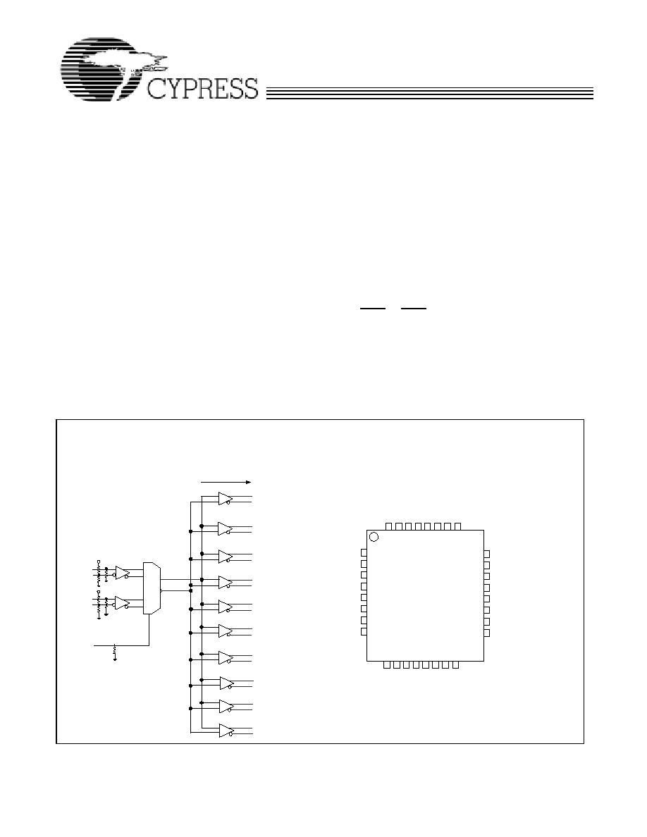
The CY2DP3110 is a low-skew, low propagation delay 2-to-10
differential fanout buffer targeted to meet the requirements of
high performance clock and data distribution applications. The
device is implemented on SiGe technology and has a fully
differential internal architecture that is optimized to achieve
low signal skews at operating frequencies of up to 3.0 GHz.
The device features two differential input paths which are
multiplexed internally. This mux is controlled by the CLK_SEL
pin. The CY2DP3110 may function not only as a differential
clock buffer but also as a signal level translator and fanout an
HSTL single-ended signal to 10 ECL/PECL differential loads.
An external bias pin, VBB, is provided for this purpose. In such
an application, the VBB pin should be connected to either one
of the CLKA or CLKB inputs and bypassed to ground via a
0.01-
µ
F capacitor.
Since the CY2DP3110 introduces negligible jitter to the timing
budget, it is the ideal choice for distributing high frequency,
high-precision clocks across back-planes and boards in
communication systems. Furthermore, advanced circuit
design schemes, such as internal temperature compensation,
ensure that the CY2DP3110 delivers consistent, guaranteed
performance over differing platforms.
Block Diagram
Pin Configuration
CLKB
Q0
Q0#
Q1
Q1#
Q2
Q2#
Q3
Q3#
Q4
Q4#
Q5
Q5#
Q6
Q6#
CLKA
CLKA#
Q8
Q8#
Q9
Q9#
Q7
Q7#
CLKB#
CLK_SEL
0
1
VCC
VCC
V
BB
CY2DP3110
VC
C
Q0
Q0
#
Q1
Q1
#
Q2
Q2
#
VC
C
VC
C
Q9
#
Q9
Q8
#
Q8
Q7
#
Q7
VC
C
Q3
Q3#
Q4
Q4#
Q5
Q5#
Q6
Q6#
VCC
CLK_SEL
CLKA
CLKA#
VBB
CLKB
CLKB#
VEE
1
2
3
4
5
6
7
8
24
23
22
21
20
19
18
17
9
10
11
12
13
14
15
16
32
31
30
29
28
27
26
25
FastEdgeTM Series
CY2DP3110
Document #: 38-07469 Rev. *D
Page 2 of 13
Governing Agencies
The following agencies provide specifications that apply to the
CY2DP3110. The agency name and relevant specification is
listed below.
Pin Description
Pin
Name
I/O
Type
Description
3,4
CLKA, CLKA# I,PD
[1]
I,PC
ECL/PECL Default differential clock input pair.
6,7
CLKB, CLKB#
I,PD
I,PC
HSTL
Alternate differential clock input pair.
2
CLK_SEL
I,PD
ECL/PECL Pull-down, selects between CLKA; pull-up for CLKB
signals.
31,29,27,24,22,20,18,1
5,13,11
Q[0-9]
O,OE
ECL/PECL True output. [mandatory RL for waveform generation]
30,28,26,23,21,19,17,1
4,12,10
Q#[0-9]
O,OE
ECL/PECL Complement output. [mandatory RL for waveform generation]
5
VBB
[3]
O
Bias
Reference voltage output for single-ended ECL or PECL
operation.
8
VEE
[2]
PWR
Power
Power supply, negative connection.
1,9,16,
25,32
VCC
+PWR
Power
Power supply, positive connection.
Control
Operation
CLK_SEL
0
Default condition (no connection to the pin)
0
CLKA, CLKA# input pair is active.
CLKA can be driven with ECL- or PECL-compatible signals with respective power configurations.
1
CLKB, CLKB# input pair is active.
CLKB can be driven by HSTL-0compatible signals with respective power configurations.
Agency Name
Specification
JEDEC
JESD 51 (Theta JA)
JESD 8-6 (HSTL)
JESD 8-2 (ECL)
JESD 65-A (skew,jitter)
IEEE
1596.3 (Jitter specs)
UL
94 (Flammability rating)
Mil-Spec
883E Method 1012.1 (Thermal Theta JC)
Notes:
1.
In the I/O column, the following notation is used: I = Input, O = Output, PD = Pull-down, PU = Pull-up, PC = Pull Center, OE = Open Emitter and PWR = Power.
2.
In ECL mode (negative power supply mode), V
EE
is either 3.3V or 2.5V and V
CC
is connected to GND (0V). In PECL mode (positive power supply mode),
V
EE
is connected to GND (0V) and V
CC
is either +3.3V or +2.5V. In both modes, the input and output levels are referenced to the most positive supply (V
CC
)
and are between V
CC
and V
EE
.
3.
V
BB
is available for use for single ended bias mode when V
CC
is +3.3V.
FastEdgeTM Series
CY2DP3110
Document #: 38-07469 Rev. *D
Page 3 of 13
Table 1. Absolute Maximum Ratings
Parameter
Description
Conditions
Min.
Max.
Unit
V
CC
Supply Voltage
Non-functional
0.3
4.6
VDC
V
CC
Operating Voltage
Functional
2.5 5%
3.3 + 5%
VDC
V
BB
Output Reference Voltage
Relative to V
CC
V
CC
1.620
V
CC
1.220
VDC
I
BB
Output Reference Current
Relative to V
BB
200
uA
VTT
Output Termination Voltage
V
CC
2
VDC
V
IN
Input Voltage
Relative to V
CC
0.3
V
CC
+ 0.3
VDC
V
OUT
Output Voltage
Relative to V
CC
0.3
V
CC
+ 0.3
VDC
LU
I
Latch Up Immunity
Functional
300
mA
T
S
Temperature, Storage
Non-functional
65
+150
°C
T
A
Temperature, Operating Ambient
Functional
40
+85
°C
Ø
Jc
Dissipation, Junction to Case
Functional
40
60
°C/W
Ø
Ja
Dissipation, Junction to Ambient
Functional
100
°C/W
ESD
h
ESD Protection (Human Body Model)
2000
Volts
M
SL
Moisture Sensitivity Level
N.A.
G
ATES
Total Functional Gate Count
Assembled Die
50
Each
FLM
Flammability Rating
V0
N.A.
Multiple Supplies: The Voltage on any input or I/O pin cannot exceed the power pin during power-up. Power supply sequencing is NOT required.
PECL/HSTL DC Specifications
(V
CC
= 2.5V ± 5%/V
CC
= 3.3 V ± 5%,V
EE
= GND, Temp. = 40
°
C
85
°
C)
Parameter
Description
Conditions
Min.
Typ.
Max.
Unit
V
IL
Input Voltage, Low
V
CC
1.945
V
CC
1.625
V
V
IH
Input Voltage, High
Define V
CC
and Load Current V
CC
1.165
V
CC
0.88
V
I
IN
Input Current
[4]
V
IN
= V
INLMIN
or V
IHMAX
|150|
uA
Clock Input Pair CLKA, CLKA (PECL Differential Signals)
V
PP
Differential Input Voltage
[5]
Differential Operation
0.1
1.3
V
V
CMR
Differential Crosspoint Voltage
[6]
Differential Operation
1.2
V
CC
V
I
IN
Input Current
[4]
V
IN
= V
ILMIN
= V
IHMAX
|150|
uA
Clock Input Pair CLKB, CLKB (HSTL Differential Signals)
V
DIF
Differential Input Voltage
[7]
0.4
1.9
V
V
X
Differential Crosspoint Voltage
[8]
0.68
0.9
V
I
IN
Input Current
V
IN
= V
X
± 0.2V
|150|
uA
PECL Outputs Q0Q9, Q0Q9 (PECL Differential Signals)
V
OL
Output Low Voltage
V
CC
= 3.3V ± 5%
V
CC
= 2.5V ± 5%
I
OL
= 5 mA
[9]
V
CC
1.945
V
CC
1.945
V
CC
1.695
V
CC
1.695
V
CC
1.5
V
CC
1.3
V
V
OH
Output High Voltage
I
OH
= 30 mA
[9]
V
CC
1.2
V
CC
0.895
V
CC
0.7
V
Notes:
4.
Inputs have internal pull-up/pull-down or biasing resistors that affect the input current.
5.
V
PP
(DC) is the minimum differential input voltage swing required to maintain device functionality.
6.
V
CMR
(DC) is the crosspoint of the differential input signal. Functional operation is obtained when the crosspoint is within the V
CMR
(DC) range and the input
swing lies within the V
PP
(DC) specification.
7.
V
DIF
(DC) is the amplitude of the differential HSTL input voltage swing required for device functionality.
8.
V
X
(DC) is the crosspoint of the differential HSTL input signal. Functional operations is obtained when the crosspoint is within the V
X
(DC) range and the input
swing lies within the V
PP
(DC) specification.
9.
Equivalent to a termination of 50
to V
TT
.
FastEdgeTM Series
CY2DP3110
Document #: 38-07469 Rev. *D
Page 4 of 13
Supply Current and V
BB
[11]
I
EE
Maximum Quiescent Supply Current
without Output Termination Current
[10]
V
EE
pin
130
mA
V
BB
Output Reference Voltage
I
BB
= 200 uA
[14]
V
CC
1.620
V
CC
1.220
V
I
PUP
Internal Pull-up Current
mA.
I
PDWN
Internal Pull-down Current
mA.
C
IN
Input Pin Capacitance
pF
C
OUT
Output Pin Capacitance
pF
L
IN
Pin Inductance
1
nH
Z
OUT
Output Impedance
ECL DC Specifications
(V
EE
= 2.5V ± 5% or V
EE
= 3.3 V± 5%, V
CC
= GND, T
A
= 40
°
C
to 85
°
C)
Parameter
Description
Conditions
Min.
Typ.
Max.
Unit
V
IL
Input Voltage, Low
1.945
1.625
V
V
IH
Input Voltage, High
Define V
CC
and Load Current
1.165
0.880
V
I
IN
Input Current
[12]
V
IN
= V
IL
or Vin = V
IH
|150|
uA
Clock Input Pair CLKA, CLKA (ECL Differential Signals)
V
PP
Differential Input Voltage
[13]
Differential Operation
0.1
1.3
V
V
CMR
Differential Crosspoint
Voltage
[14]
Differential Operation
V
EE
+ 1.2
0V
V
I
IN
Input Current
[12]
V
IN
= V
IL
or V
IN
= V
IH
|150|
uA
ECL Outputs Q0Q9, Q0Q9 (ECL Differential Signals)
[15]
V
OH
Output High Voltage
I
OH
= 30 mA
[16]
1.2
0.7
V
V
OL
Output Low Voltage
V
EE
= 2.5V ± 5%
V
EE
= 3.3V ± 5%
I
OL
= 5 ma
[16]
1.945
1.945
1.695
1.695
1.3
1.5
V
V
Supply Current and V
BB
I
EE
Maximum Quiescent Supply
Current without Output
Termination Current
[17]
V
EE
Pin
130
mA
V
BB
Output Reference Voltage
I
BB
= 200 uA
1.525
1.325
V
Table 2. Timing Specifications
Parameter
Description
Conditions
Min.
Typ.
Max.
Unit
TTB
Total Timing Budget
500-MHz 50% Duty Cycle Standard Load
250
ps
D
j
Deterministic/Intrinsic Jitter
500-MHz 50% Duty Cycle Standard Load
1
ps r.m.s.
Notes:
10. I
CC
calculation: I
CC
= (number of differential output pairs used) x (I
OH
+ I
OL
) + I
EE
orI
CC
= (number of differential output pairs used) x (V
OH
VTT)/Rload + (V
OL
V
TT
)/Rload +I
EE
.
11. V
BB
is limited to V
CC
of 3.3V only. See note 20.
12. Input have internal pull-up/pull-down or biasing resistors which affect the input current.
13. V
PP
(DC) is the minimum differential input voltage swing required to maintain device functionality
14. V
CMR
(DC) is the crosspoint of the differential input signal. Functional operation is obtained when the crosspoint is within the V
CMR
(DC) range and the input
swing lies within the V
PP
(DC) specification.
15. Standard ECL down to 2.5V, Cypress part operates down to 3.3V
16. Equivalent to a termination of 50
to VTT.
17. I
CC
Calculation: I
CC
= (number of differential output pairs used) x (I
OH
+ I
OL
) + IEE or I
CC
= (number of differential output pairs used) x (V
OH
VTT)/Rload +
(V
OL
V
TT
)/Rload +I
EE
.
PECL/HSTL DC Specifications
(V
CC
= 2.5V ± 5%/V
CC
= 3.3 V ± 5%,V
EE
= GND, Temp. = 40
°
C
85
°
C) (continued)
Parameter
Description
Conditions
Min.
Typ.
Max.
Unit
FastEdgeTM Series
CY2DP3110
Document #: 38-07469 Rev. *D
Page 5 of 13
Table 3. Jitter
0000 0101 0100 1100 1100 1100 0111 0001 1100 0111 0101
PRBS 44-bit (9 44-bit Binary streams before loopback)
Freq (MHz)
Neg Max (ps)
Pos Max (ps)
Peak-Peak (ps)
R.M.S (ps)
270.00
0.117
0.16
0.277
0.116
333.00
0.471
0.44
0.911
0.101
500.00
0.261
0.276
0.537
0.065
550.00
0.26
0.232
0.492
0.61
CLOCK
500
0.136
0.109
0.245
0.059
AC Specifications
([ECL:V
EE
= 3.3 V
DC
± 5% or V
EE
= 2.5V±5%, V
CC
= GND] or [HSTL/PECL:V
CC
= 3.3V ± 5% or V
CC
= 2.5V ±5%, V
EE
= GND] Temp. = 40
°
C
to 85
°
C)
[18]
Parameter
Description
Conditions
Min.
Typ.
Max.
Unit
Clock Input Pair CLKA, CLKA (PECL or ECL Differential Signals)
V
PP
Differential Input Voltage
[19]
Differential Operation
0.1
1.3
V
V
CMR
Differential Crosspoint Voltage
[20]
Differential Operation
VEE+1.2
0V
V
F
CLK
Input Frequency
[21]
50% duty cycle Standard load
2200
MHz
T
PD
Propagation Delay CLKA or CLKB to
Q0Q9 Pair
660-MHz 50% Duty Cycle Standard
Load Differential Operation
280
400
650
ps
Clock Input Pair CLKB, CLKB (HSTL Differential Signals)
V
DIF
Differential Input Voltage
[22]
Duty Cycle Standard Load Differ-
ential Operation
0.4
1.9
V
V
X
Differential Crosspoint Voltage
[23]
Standard Load Differential
Operation
0.68
0.9
V
F
CLK
Input Frequency
2200
MHz
T
PD
Propagation Delay CLKA or CLKB to
Q0Q9 Pair
<1-GHz Differential
280
400
750
ps
ECL Clock Outputs (Q09, Q09) (Differential)
Vo
(P-P)
Differential Output Voltage
(Peak-to-Peak)
Differential PRBS
fo < 50 MHz
fo < 0.8 GHz
fo < 1.0 GHz
fo < 1.5 GHz
fo < 2.2 GHz
0.45
0.4
0.375
0.34
0.30
V
tsk(o)
Output-to-Output Skew
660-MHz 50% Duty Cycle Standard
Load Differential Operation
50
ps
tsk(PP)
Output-to-Output Skew (part-to-part) 660-MHz 50% Duty Cycle Standard
Load Differential Operation
500
ps
tJIT(CC)
Output Cycle-to-Cycle Jitter
(Intrinsic) RMS
500-MHz 50% Duty Cycle Standard
Load Differential Operation
1
ps
tsk(P)
Output Pulse Skew
[24]
660-MHz 50% Duty Cycle Standard
Load Differential Operation
50
ps
tr, tf
Output Rise/Fall time
660-MHz 50% Duty Cycle Differ-
ential 20% to 80%
0.3
ns
18. AC characteristics apply for parallel output termination of 50
to V
TT
.
19. V
PP
(AC) is the minimum differential ECL/PECL input swing required to maintain AC characteristics including tpd and device-to-device skew.
20. V
CMR
(AC) is the crosspoint of the differential ECL/PECL input signal. Normal AC operation is obtained when the crosspoint is within the V
CMR
(AC) range and
the input swing lies within the V
PP
(AC) specification. Violation of V
CMR
(AC) or V
PP
(AC) impacts the device propagation delay, device and part-to-part skew.
21. The CY2DP3110 is fully operational up to 1.5GHz with full PECL swing. Reduced swing up to 2.2 GHz.
22. V
DIF
(AC) is the minimum differential HSTL input voltage swing required to maintain AC characteristics including tkpd and device-to-device skew
23. V
X
(AC) is the crosspoint of the differential HSTL input signal. Normal AC operation is obtained when the crosspoint is within the V
X
(AC) range and the input
swing lies within the V
DIF
(AC) specification. Violation of V
X
(AC) or V
DIF
(AC) impacts the device propagation delay, device and part-to-part skew.
24. Output pulse skew is the absolute difference of the propagation delay times: | tPLH tPHL |.