 | –≠–ª–µ–∫—Ç—Ä–æ–Ω–Ω—ã–π –∫–æ–º–ø–æ–Ω–µ–Ω—Ç: CY25245 | –°–∫–∞—á–∞—Ç—å:  PDF PDF  ZIP ZIP |
Frequency-multiplying, Peak-reducing
EMI Solution
CY25245
Cypress Semiconductor Corporation
∑
3901 North First Street
∑
San Jose
,
CA 95134
∑
408-943-2600
Document #: 38-07124 Rev. *B
Revised February 2, 2005
Features
∑ Cypress PREMISTM SMARTSPREADTM family offering
∑ Generates an electromagnetic interference (EMI)
optimized clocking signal at the output
∑ Selectable output frequency range
∑ Single 1.25%, 2.5%, 5%, or 10% down or center spread
output
∑ Integrated loop filter components
∑ Operates with a 3.3 or 5V supply
∑ Low power CMOS design
∑ Available in 20-pin Small Shrunk Outline Package
(SSOP)
Key Specifications
Supply voltages: .......................................V
DD
= 3.3V ± 0.3V
or V
DD
= 5V ± 10%
Frequency range:............................ 13 MHz
F
in
166 MHz
Cycle-to-cycle jitter: ......................................... 250 ps (max)
Output duty cycle: ................................ 40/60% (worst case)
Notes:
1. Pins marked with ^ are internal pull-down resistors with weak 250 k
.
2. Pins marked with * are internal pull-up resistors with weak 80 k
.
CY2
5245
20
19
18
17
1
2
3
4
X1
X2
AVDD
MW0^
REFOUT
VDD
GND
IR1*
5
6
7
14
15
16
IR2*
SSOUT
MW1*
SDATA
OR1^
8
9
10
11
12
13
VDD
MW2^
OR2*
SSON#^
GND
GND
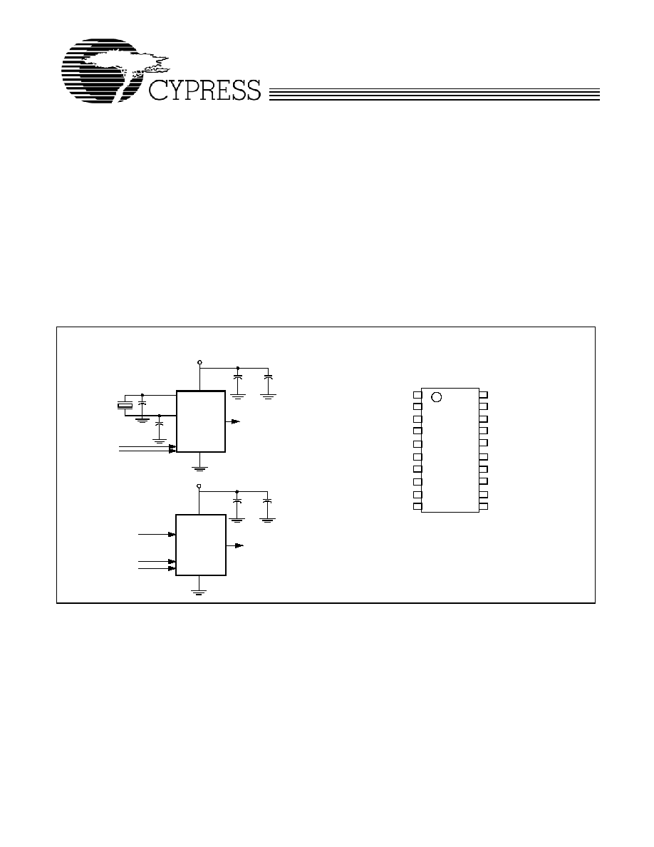
Simplified Block Diagram
Pin Configuration
SSOP
Spread Spectrum
CY25245
(EMI suppressed)
3.3V or 5.0V
Oscillator or
Spread Spectrum
CY25245
(EMI suppressed)
3.3V or 5.0V
XTAL
X1
X2
Reference Input
Input
Output
Output
X1
SCLK
SDATA
SDATA
SCLK
Serial Interface
Serial Interface
SCLK
[1, 2]

CY25245
Document #: 38-07124 Rev. *B
Page 2 of 11
Pin Definitions
Pin Name Pin No. Pin Type
Pin Description
SSOUT
15
O
Output Modulated Frequency. Frequency modulated copy of the input clock (SSON# asserted).
REFOUT
20
O
Non-modulated Output. This pin provides a copy of the reference frequency. This output will
not have the Spread Spectrum feature enabled regardless of the state of logic input SSON#.
X1
1
I
Crystal Connection or External Reference Frequency Input. This pin has dual functions. It
may either be connected to an external crystal, or to an external reference clock.
X2
2
I
Crystal Connection. Input connection for an external crystal. If using an external reference, this
pin must be left unconnected.
SSON#
10
I
Spread Spectrum Control (Active LOW). Asserting this signal (active LOW) turns the internal
modulation waveform on. This pin has an internal pull-down resistor.
MW0:2
4, 11, 14
I
Modulation Width Selection. When Spread Spectrum feature is turned on, these pins are used
to select the amount of variation and peak EMI reduction that is desired on the output signal.
MW0:Down, MW1:Up, MW2:Down (see Table 2).
IR1:2
17, 16
I
Reference Frequency Selection. The logic level provided at this input indicates to the internal
logic what range the reference frequency is in and determines the factor by which the device
multiplies the input frequency. Refer to Table 3. These pins have internal pull-up resistors.
OR1:2
6, 9
I
Output Frequency Selection Bits. These pins select the frequency operation for the output.
Refer to Table 1. The OR2 pin has an internal pull-up resistor. The OR1 pin has internal pull-down
resistors.
SCLK
7
I
Clock Pin for SMBus Circuitry.
SData
5
I/O
Data Pin for SMBus Circuitry.
VDD
12, 19
P
Power Connection. Connected to 3.3V or 5V power supply.
AVDD
3
P
Analog Power Connection. Connected to 3.3V or 5V power supply.
GND
8, 13, 18
G
Ground Connection. Connect all ground pins to the common ground plane.
Table 1. Frequency Configuration (Frequencies in MHz)
Range of Fin Frequency
Multiplier
Settings
Output/
Input
Range of Fout Required R Settings
Modulation and
Power-down Settings
Min.
Max.
OR2
OR1
Min.
Max.
IR2
IR1
MW2
MW1
14
41.7
0
1
1
14
41.7
0
1
Table 2
14
41.7
1
0
2
28
83.3
0
1
Table 2
14
41.7
1
1
4
56
166
0
1
Table 2
25
83.3
0
1
0.5
13
41.7
1
0
Table 2
25
83.3
1
0
1
25
83.3
1
0
Table 2
25
83.3
1
1
2
50
166
1
0
Table 2
50
166
0
1
0.25
13
41.7
1
1
Table 2
50
166
1
0
0.5
25
83.3
1
1
Table 2
50
166
1
1
1
50
166
1
1
Table 2
Reserved
0
0
N/A
N/A
N/A
As Set
As Set
1
0
Power-down Hi-Z
0
0
N/A
N/A
N/A
As Set
As Set
1
1
Power-down 0
0
0
N/A
N/A
N/A
As Set
As Set
0
0
Power-down 1
0
0
N/A
N/A
N/A
As Set
As Set
0
1

CY25245
Document #: 38-07124 Rev. *B
Page 3 of 11
Overview
The CY25245 product is one of a series of devices in the
Cypress PREMIS family. The PREMIS family incorporates the
latest advances in PLL spread spectrum frequency synthe-
sizer techniques. By frequency modulating the output with
a low-frequency carrier, peak EMI is greatly reduced. Use of
this technology allows systems to pass increasingly difficult
EMI testing without resorting to costly shielding or redesign.
In a system, not only is EMI reduced in the various clock lines,
but also in all signals which are synchronized to the clock.
Therefore, the benefits of using this technology increase with
the number of address and data lines in the system. The
Simplified Block Diagram shows a simple implementation.
Functional Description
The CY25245 uses a phase-locked loop (PLL) to frequency
modulate an input clock. The result is an output clock whose
frequency is slowly swept over a narrow band near the input
signal. The basic circuit topology is shown in Figure 1. The
input reference signal is divided by Q and fed to the phase
detector. A signal from the VCO is divided by P and fed back
to the phase detector also. The PLL will force the frequency of
the VCO output signal to change until the divided output signal
and the divided reference signal match at the phase detector
input. The output frequency is then equal to the ratio of P/Q
times the reference frequency.
[3]
The unique feature of the
Spread Spectrum Frequency Timing Generator is that a
modulating waveform is superimposed at the input to the VCO.
This causes the VCO output to be slowly swept across a
predetermined frequency band.
Because the modulating frequency is typically 1000 times
slower than the fundamental clock, the spread spectrum
process has little impact on system performance.
Frequency Selection With SSFTG
In spread spectrum frequency timing generation, EMI
reduction depends on the shape, modulation percentage, and
frequency of the modulating waveform. While the shape and
frequency of the modulating waveform are fixed for a given
frequency, the modulation percentage may be varied.
Using frequency select bits (FS2:1 pins), the frequency range
can be set (see Table 2). Spreading percentage is set with pins
MW0:2 as shown in Table 2.
A larger spreading percentage improves EMI reduction.
However, large spread percentages may either exceed
system maximum frequency ratings or lower the average
frequency to a point where performance is affected. For these
reasons, spreading percentage options are provided.
Note:
3. For the CY25245, the output frequency is nominally equal to the input frequency.
Table 2. Modulation Width Selection Table
EMI Reduction
Modulation Setting
Bandwith Limit Frequencies as a % Value of Fout
MW0 = 0
MW0 = 1
MW2
MW1
Low
High
Low
High
Minimum EMI Control
0
0
98.75%
100%
99.375%
100.625%
Suggested Setting
0
1
97.5%
100%
98.75%
101.25%
Alternate Setting
1
0
95.0%
100%
97.5%
102.5%
Maximum EMI reduction
1
1
90.0%
100%
95%
105%
Freq.
Phase
Modulating
VCO
Post
CLKOUT
Detector
Charge
Pump
Waveform
Dividers
Divider
Feedback
Divider
PLL
GND
V
DD
Q
P
Clock Input
Reference Input
(EMI suppressed)
Figure 1. Functional Block Diagram

CY25245
Document #: 38-07124 Rev. *B
Page 4 of 11
Spread Spectrum Frequency Timing Generator
The device generates a clock that is frequency modulated in
order to increase the bandwidth that it occupies. By increasing
the bandwidth of the fundamental and its harmonics, the ampli-
tudes of the radiated electromagnetic emissions are reduced.
This effect is depicted in Figure 2.
As shown in Figure 2, a harmonic of a modulated clock has a
much lower amplitude than that of an unmodulated signal. The
reduction in amplitude is dependent on the harmonic number
and the frequency deviation or spread.
The output clock is modulated with a waveform depicted in
Figure 3. This waveform, as discussed in "Spread Spectrum
Clock Generation for the Reduction of Radiated Emissions" by
Bush, Fessler, and Hardin, produces the maximum reduction
in the amplitude of radiated electromagnetic emissions. The
deviation selected for this chip is as described in Table 2.
Figure 3 details the Cypress spreading pattern. Cypress does
offer options with more spread and greater EMI reduction.
Contact your local Sales representative for details on these
devices.
Spread
Spectrum
Enabled
EMI Reduction
Spread
Spectrum
Non-
Frequency Span (MHz)
Down Spread
A
m
pl
itude (dB
)
Figure 2. Clock Harmonic with and without SSCG Modulation Frequency Domain Representation
MAX.
MIN.
10
%
20
%
30
%
40
%
50
%
60
%
70
%
80
%
90
%
100
%
10
%
20
%
30
%
40
%
50
%
60
%
70
%
80
%
90
%
100
%
FREQUENCY
Figure 3. Typical Modulation Profile

CY25245
Document #: 38-07124 Rev. *B
Page 5 of 11
Serial Data Interface
The CY25245 features a two-pin, serial data interface that can
be used to configure internal register settings that control
particular device functions. Upon power-up, the CY25245
initializes with default register settings, therefore the use of this
serial data interface is optional. The serial interface is
write-only (to the clock chip) and is the dedicated function of
device pins SDATA and SCLOCK. In motherboard applica-
tions, SDATA and SCLOCK are typically driven by two logic
outputs of the chipset. Clock device register changes are
normally made upon system initialization, if any are required.
The interface can also be used during system operation for
power management functions. Table 3 summarizes the control
functions of the serial data interface.
Operation
Data is written to the CY25245 in eleven bytes of eight bits
each. Bytes are written in the order shown in Table 4.
Writing Data Bytes
Each bit in Data Bytes 0≠7 control a particular device function
except for the "reserved" bits which must be written as a logic
0. Bits are written MSB (most significant bit) first, which is bit 7.
Table 5 gives the bit formats for registers located in Data Bytes
0≠7.
Table 3. Serial Data Interface Control Functions Summary
Control Function
Description
Common Application
Clock Output Disable Any individual clock output(s) can be disabled.
Disabled outputs are actively held LOW.
Unused outputs are disabled to reduce EMI and
system power. Examples are clock outputs to unused
PCI slots.
CPU Clock Frequency
Selection
Provides CPU/PCI frequency selections through
software. Frequency is changed in a smooth and
controlled fashion.
For alternate microprocessors and power
management options. Smooth frequency transition
allows CPU frequency change under normal system
operation.
Spread Spectrum
Enabling
Enables or disables spread spectrum clocking.
For EMI reduction.
Output three-state
Puts clock output into a high-impedance state.
Production PCB testing.
(Reserved)
Reserved function for future device revision or
production device testing.
No user application. Register bit must be written as 0.
Table 4. Byte Writing Sequence
Byte
Sequence
Byte Name
Bit Sequence
Byte Description
1
Slave Address
11010010
Commands the CY25245 to accept the bits in Data Bytes 0≠6 for internal register
configuration. Since other devices may exist on the same common serial data
bus, it is necessary to have a specific slave address for each potential receiver.
The slave receiver address for the CY25245 is 11010010. Register setting will
not be made if the Slave Address is not correct (or is for an alternate slave
receiver).
2
Command Code Don't Care
Unused by the CY25245, therefore bit values are ignored ("don't care"). This byte
must be included in the data write sequence to maintain proper byte allocation.
The Command Code Byte is part of the standard serial communication protocol
and may be used when writing to another addressed slave receiver on the serial
data bus.
3
Byte Count
Don't Care
Unused by the CY25245, therefore bit values are ignored ("don't care"). This byte
must be included in the data write sequence to maintain proper byte allocation.
The Byte Count Byte is part of the standard serial communication protocol and may
be used when writing to another addressed slave receiver on the serial data bus.
4
Data Byte 0
Refer to Table 5 The data bits in Data Bytes 0≠7 set internal CY25245 registers that control device
operation. The data bits are only accepted when the Address Byte bit sequence
is 11010010, as noted above. For description of bit control functions, refer to
Table 5, Data Byte Serial Configuration Map.
5
Data Byte 1
6
Data Byte 2
7
Data Byte 3
8
Data Byte 4
9
Data Byte 5
10
Data Byte 6
11
Data Byte 7