 | –≠–ª–µ–∫—Ç—Ä–æ–Ω–Ω—ã–π –∫–æ–º–ø–æ–Ω–µ–Ω—Ç: B9946 | –°–∫–∞—á–∞—Ç—å:  PDF PDF  ZIP ZIP |

3.3V, 160-MHz, 1:10 Clock Distribution Buffer
B9946
Cypress Semiconductor Corporation
∑
3901 North First Street
∑
San Jose
∑
CA 95134
∑
408-943-2600
Document #: 38-07077 Rev. *C
Revised December 22, 2002
Product Features
∑ 160-MHz Clock Support
∑ LVCMOS/LVTTL Compatible Inputs
∑ 10 Clock Outputs: Drive up to 20 Clock Lines
∑ 1X or 1/2X Configurable Outputs
∑ Output Three-state Control
∑ 250 ps Maximum Output-to-Output Skew
∑ Pin Compatible with MPC946
∑ Industrial Temp. Range: ≠40∞C to +85∞C
∑ 32-Pin TQFP Package
Description
The B9946 is a low-voltage clock distribution buffer with the
capability to select one of two LVCMOS/LVTTL compatible in-
put clocks. These clock sources can be used to provide for test
clocks as well as the primary system clocks. All other control
inputs are LVCMOS/LVTTL compatible. The 10 outputs are
3.3V LVCMOS or LVTTL compatible and can drive two series
terminated 50
transmission lines. With this capability the
B9946 has an effective fanout of 1:20.
The B9946 is capable of generating 1X and 1/2X signals from
a 1X source. These signals are generated and retimed inter-
nally to ensure minimal skew between the 1X and 1/2X sig-
nals. SEL(A:C) inputs allow flexibility in selecting the ratio of
1X to1/2X outputs.
The B9946 outputs can also be three-stated via MR/OE# in-
put. When MR/OE# is set HIGH, it resets the internal flip-flops
and three-states the outputs.
B9946
MR
/O
E#
VSS
QA
0
V
DDC
QA
1
VSS
QA
2
V
DDC
V
DDC
QC0
VSS
QC1
V
DDC
QC2
VSS
QC3
VSS
QB0
VDDC
QB1
VSS
QB2
VDDC
VDDC
TCLK_SEL
VDD
TCLK0
TCLK1
DSELA
DSELB
DSELC
VSS
1
2
3
4
5
6
7
8
24
23
22
21
20
19
18
17
9
10
11
12
13
14
15
16
32
31
30
29
28
27
26
25
3
QA0:2
3
QB0:2
4
QC0:3
0
1
0
1
0
1
0
1
/1
/2
R
TCLK0
TCLK_SEL
TCLK1
DSELA
DSELB
DSELC
MR/OE#
Block Diagram
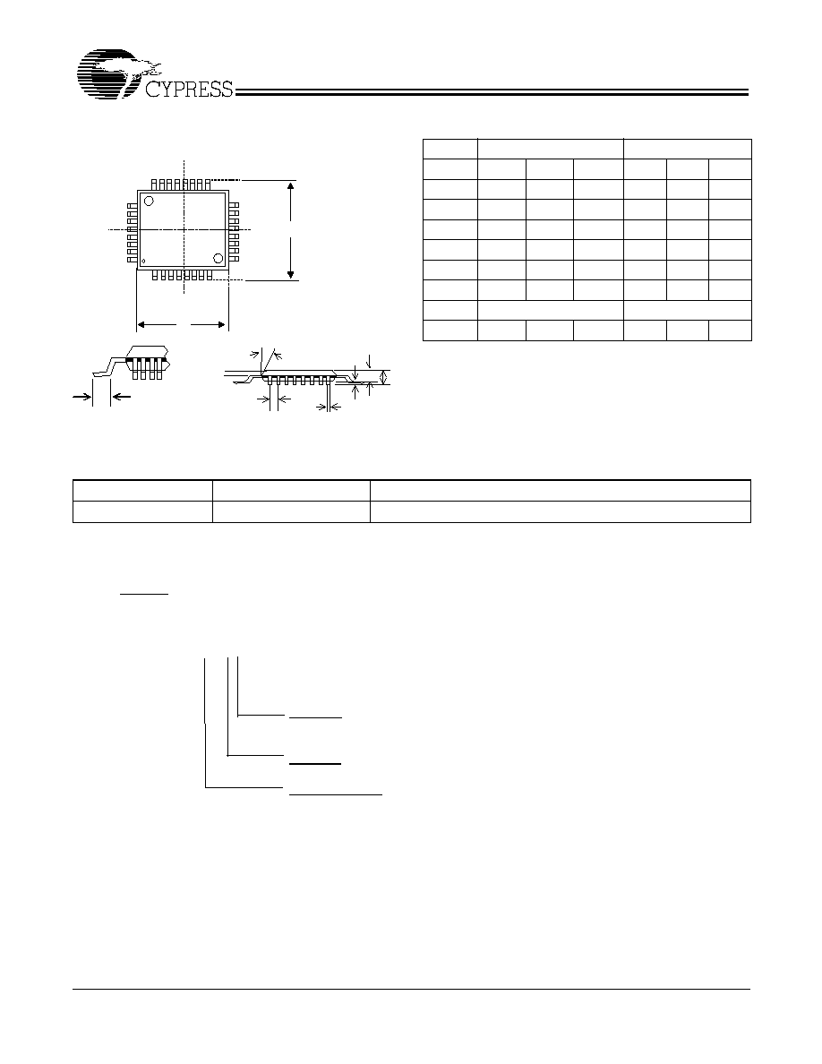
Pin Configuration

B9946
Document #: 38-07077 Rev. *C
Page 2 of 5
Note:
1.
PD = Internal Pull-Down, PU = Internal Pull-Up.
Pin Description
[1]
Pin
Name
PWR
I/O
Description
3, 4
TCLK(0,1)
I, PU
External Reference/Test Clock Input
26, 28, 30
QA(2:0)
VDDC
O
Clock Outputs
19, 21, 23
QB(2:0)
VDDC
O
Clock Outputs
10, 12, 14, 16
QC(0:3)
VDDC
O
Clock Outputs
5, 6, 7
DSEL(A:C)
I, PD
Divider Select Inputs. When HIGH, selects
˜
2 input divider. When
LOW, selects
˜
1 input divider.
1
TCLK_SEL
I, PD
TCLK Select Input. When LOW, TCLK0 clock is selected and when
HIGH TCLK1 is selected.
32
MR/OE#
I, PD
Output Enable Input. When asserted LOW, the outputs are enabled
and when asserted HIGH, internal flip-flops are reset and the out-
puts are three-stated.
9, 13, 17, 18, 22,
25, 29
VDDC
3.3V Power Supply for Output Clock Buffers
2
VDD
3.3V Power Supply
8, 11, 15, 20, 24,
27, 31
VSS
Common Ground

B9946
Document #: 38-07077 Rev. *C
Page 3 of 5
Maximum Ratings
[2]
Maximum Input Voltage Relative to V
SS
: ............ V
SS
≠ 0.3V
Maximum Input Voltage Relative to V
DD
: ............. V
DD
+ 0.3V
Storage Temperature: ................................≠65∞C to + 150∞C
Operating Temperature: ................................ ≠40∞C to +85∞C
Maximum ESD Protection.............................................. 2 KV
Maximum Power Supply: ................................................5.5V
Maximum Input Current:
..................................................±
20 mA
This device contains circuitry to protect the inputs against
damage due to high static voltages or electric field; however,
precautions should be taken to avoid application of any volt-
age higher than the maximum rated voltages to this circuit. For
proper operation, V
in
and V
out
should be constrained to the
range:
V
SS
< (V
in
or V
out
) < V
DD
Unused inputs must always be tied to an appropriate logic volt-
age level (either V
SS
or V
DD
).
Notes:
2.
The voltage on any input or I/O pin cannot exceed the power pin during power-up. Power supply sequencing is NOT required.
3.
Inputs have pull-up/pull-down resistors that effect input current.
4.
Driving series or parallel terminated 50
(or 50
to V
DD
/2) transmission lines.
5.
Parameters are guaranteed by design and characterization. Not 100% tested in production. All parameters specified with loaded outputs.
6.
Outputs driving 50
transmission lines.
7.
50% input duty cycle.
8.
Outputs loaded with 30 pF each
9.
Part-to-Part skew at a given temperature and voltage.
DC Parameters:
V
DDC
= 3.3V ±10%, V
DD
= 3.3V ±10%, T
A
= ≠40∞C to +85∞C
Parameter
Description
Conditions
Min.
Typ.
Max.
Unit
V
IL
Input Low Voltage
V
SS
0.8
V
V
IH
Input High Voltage
2.0
V
DD
V
I
IL
Input Low Current (@V
IL
= V
SS
)
Note 3
≠100
µA
I
IH
Input High Current (@V
IL
=V
DD
)
100
µA
V
OL
Output Low Voltage
I
OL
= 20 mA, Note 4
0.4
V
V
OH
Output High Voltage
I
OH
= ≠20 mA, V
DDC
= 3.3V, Note 4
2.5
V
I
DD
Quiescent Supply Current
All V
DDC
and V
DD
-
1
2
mA
C
in
Input Capacitance
-
-
4
pF
AC Parameters
[5]
:
V
DDC
= 3.3V ±10%, V
DD
= 3.3V ±10%, T
A
= ≠40∞C to +85∞C
Parameter
Description
Conditions
Min.
Typ.
Max.
Unit
Fmax
Maximum Input Frequency
[6]
160
MHz
Tpd
TTL_CLK to Q Delay
[6]
5.0
-
11.5
ns
FoutDC
Output Duty Cycle
[6,7]
Measured at V
DDC
/2
TCYCLE/2 ≠ 1
TCYCLE/2 + 1
ns
tpZL, tpZH
Output enable time (all outputs)
2
10
ns
tpLZ, tpHZ
Output disable time (all outputs)
2
10
ns
Tskew
Output-to-Output Skew
[6,8]
250
ps
Tskew(pp)
Part-to-Part Skew
[9]
2.0
4.5
ns
Tr/Tf
Output Clocks Rise/Fall Time
[8]
0.8V to 2.0V
0.10
1.0
ns
B9946
Document #: 38-07077 Rev. *C
Page 4 of 5
© Cypress Semiconductor Corporation, 2001. The information contained herein is subject to change without notice. Cypress Semiconductor Corporation assumes no responsibility for the use
of any circuitry other than circuitry embodied in a Cypress Semiconductor product. Nor does it convey or imply any license under patent or other rights. Cypress Semiconductor does not authorize
its products for use as critical components in life-support systems where a malfunction or failure may reasonably be expected to result in significant injury to the user. The inclusion of Cypress
Semiconductor products in life-support systems application implies that the manufacturer assumes all risk of such use and in doing so indemnifies Cypress Semiconductor against all charges.
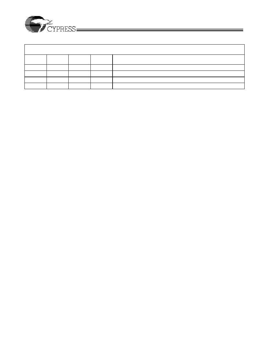
Package Drawing and Dimensions
Note:
10. The ordering part number is formed by a combination of device number, device revision, package style, and screening as shown below.
D
D
1
A
2
b
e
10
∞
A
L
A
1
32-Pin TQFP Outline Dimensions
Inches
Millimeters
Symbol
Min.
Nom.
Max.
Min.
Nom.
Max.
A
-
-
0.047
-
-
1.20
A
1
0.002
-
0.006
0.05
-
0.15
A2
0.037
-
0.041
0.95
-
1.05
D
-
0.354
-
-
9.00
-
D
1
-
0.276
-
-
7.00
-
b
0.012
-
0.018
0.30
-
0.45
e
0.031 BSC
0.80 BSC
L
0.018
-
0.030
0.45
0
0.75
Ordering Information
Part Number
[10]
Package Type
Production Flow
B9946CA
32-Pin TQFP
Industrial, ≠40∞C to +85∞C
Marking: Example:
Cypress
B9946CA
Date Code, Lot #
B9946CA
Package
A = TQFP
Revision
Device Number
B9946
Document #: 38-07077 Rev. *C
Page 5 of 5
Document Title: B9946 3.3V, 160-MHz, 1:10 Clock Distribution Buffer
Document Number: 38-07077
REV.
ECN NO.
Issue
Date
Orig. of
Change
Description of Change
**
107113
06/06/01
IKA
Convert from IMI to Cypress
*A
108057
07/03/01
NDP
Changed Commercial to Industrial (See page 4)
*B
109803
01/31/02
DSG
Convert from Word to Frame
*C
122762
12/22/02
RBI
Add power up requirements to maximum ratings information