 | –≠–ª–µ–∫—Ç—Ä–æ–Ω–Ω—ã–π –∫–æ–º–ø–æ–Ω–µ–Ω—Ç: CAT660 | –°–∫–∞—á–∞—Ç—å:  PDF PDF  ZIP ZIP |

1
FEATURES
I
Replaces MAX660 and LTCÆ660
I
Converts V+ to V- or V+ to 2V+
I
Low output resistance, 4
typical
I
High power efficiency
I
Selectable charge pump frequency
- 10kHz or 80kHz
- Optimize capacitor size
DESCRIPTION
The CAT660 is a charge-pump voltage converter. It will
invert a 1.5V to 5.5V input to a -1.5V to -5.5V output. Only
two external capacitors are needed. With a guaranteed
100mA output current capability, the CAT660 can replace
a switching regulator and its inductor. Lower EMI is
achieved due to the absence of an inductor.
In addition, the CAT660 can double a voltage supplied
from a battery or power supply. Inputs from 2.5V to 5.5V
will yield a doubled, 5V to 11V output voltage.
A Frequency Control pin (BOOST/FC) is provided to
select either a high (80kHz) or low (10kHz) internal
oscillator frequency, thus allowing quiescent current vs.
capacitor size trade-offs to be made. The 80kHz
frequency is selected when the FC pin is connected to
CAT660
100mA CMOS Charge Pump Inverter/Doubler
I
Low quiescent current
I
Pin-compatible, high-current alternative to
7660/1044
I
Industrial temperature range
I
Available in 8-pin SOIC, DIP and 0.8mm thin 8-
pad TDFN packages
- Lead-free, halogen-free package option
© 2005 by Catalyst Semiconductor, Inc.
Characteristics subject to change without notice
Doc. No. 5000, Rev. U
APPLICATIONS
I
Negative voltage generator
I
Voltage doubler
I
Voltage splitter
Preliminary Information
I
Low EMI power source
I
GaAs FET biasing
I
Lithium battery power supply
I
Instrumentation
I
LCD contrast bias
I
Cellular phones, pagers
TYPICAL APPLICATION
V+. The operating frequency can also be adjusted with
an external capacitor at the OSC pin or by driving OSC
with an external clock.
Both 8-pin DIP and SOIC packages are available in the
industrial temperature range. The TDFN package has a
4x4mm footprint and features a 0.8mm maximum height.
Compared to the 8-pin SOIC the TDFN package footprint
is nearly 50% less. For die availability, contact Catalyst
Semiconductor marketing.
The CAT660 replaces the MAX660 and the LTC
660.
In addition, the CAT660 is pin compatible with the 7660/
1044, offering an easy upgrade for applications with
100mA loads.
HA
LOGEN FREE
TM
LEAD FREE
8
7
6
5
1
2
3
4
BOOST/FC
CAP+
GND
CAP-
V+
OSC
LV
OUT
CAT660
+VIN
1.5V to 5.5V
Inverted
Negative
Output
Voltage
+
VOLTAGE INVERTER
8
7
6
5
1
2
3
4
Doubled
Positive
Output
Voltage
+
VIN = 2.5V to 5.5V
BOOST/FC
CAP+
GND
CAP-
V+
OSC
LV
OUT
POSITIVE
VOLTAGE DOUBLER
C1
C1
CAT660

CAT660
2
Doc. No. 5000, Rev. U
8
7
6
5
1
2
3
4
BOOST/FC
CAP+
GND
CAP-
V+
OSC
LV
OUT
CAT
660
8
7
6
5
1
2
3
4
BOOST/FC
CAP+
GND
CAP-
V+
OSC
LV
OUT
CAT
660
PIN DESCRIPTIONS
Circuit Configuration
Pin Number
Name
Inverter Mode
Doubler Mode
Boost/FC
Oscillator Frequency
Open
10kHz typical
V+
80kHz typical, 40kHz minimum
2
CAP+
Charge pump capacitor. Positive terminal.
Same as inverter.
3
GND
Power supply ground.
Power supply. Positive voltage input.
4
CAP-
Charge pump capacitor. Negative terminal.
Same as inverter.
5
OUT
Output for negative voltage.
Power supply ground.
6
LV
LV must be tied to OUT for all input
voltages.
8
V+
Power supply. Positive voltage input.
Positive voltage output.
Frequency Control for the internal oscilla-
tor. With an external oscillator BOOST/FC
has no effect.
Same as inverter.
Low-Voltage selection pin. When the input
voltage is less than 3V, connect LV to GND.
For input voltages above 3V, LV may be
connected to GND or left open. If OSC is
driven externally, connect LV to GND.
Oscillator control input. An external capacitor
can be connected to lower the oscillator
frequency. An external oscillator can drive
OSC and set the chip operating frequency.
The charge-pump frequency is one-half the
frequency at OSC.
Same as inverter. Do not overdrive
OSC in doubling mode. Standard logic
levels will not be suitable. See the
applications section for additional
information.
7
OSC
Oscillator Frequency
10kHz typical, 5kHz minimum
80kHz typical, 40kHz minimum
1 Boost/FC
PIN CONFIGURATION
8
7
6
5
1
2
3
4
BOOST/FC
CAP+
GND
CAP-
V+
OSC
LV
OUT
CAT
660
(Top View)
TDFN Package: 4mm x 4mm
0.8mm maximum height
SOIC Package (S, X)
TDFN Package (RD8, ZD8)
DIP Package (P)
ORDERING INFORMATION
Part Number
Package
Temperature Range
CAT660EPA
8 lead Plastic DIP
-40
∞C to 85∞C
CAT660ESA
8-lead SOIC
-40
∞C to 85∞C
CAT660ESA-TE13
8-lead SOIC, Tape & Reel
-40
∞C to 85∞C
CAT660ERD8
8-pad TDFN
-40
∞C to 85∞C
CAT660EVA
8-lead SOIC (Lead-free, Halogen-free)
-40
∞C to 85∞C
CAT660EVA-TE13
8-lead SOIC (Lead-free, Halogen-free)
-40
∞C to 85∞C
CAT660EZD8
8-pad TDFN (Lead-free, Halogen-free)
-40
∞C to 85∞C
(Top View)
(Top View)

CAT660
3
Doc. No. 5000, Rev. U
ABSOLUTE MAXIMUM RATINGS
V+ to GND ............................................................. 6V
Input Voltage (Pins 1, 6 and 7) .. -0.3V to (V+ + 0.3V)
BOOST/FC and OSC Input Voltage ........... The least
negative of (Out - 0.3V) or (V+ - 6V) to (V+ + 0.3V)
Output Short-circuit Duration to GND .............. 1 sec.
(OUT may be shorted to GND for 1 sec without damage but
shorting OUT to V+ should be avoided.)
Continuous Power Dissipation (T
A
= 70
∞C)
Plastic DIP ................................................ 730mW
SOIC ......................................................... 500mW
TDFN ............................................................... 1W
Operating Ambient Temperature Range
CAT660E .............. -40
∞C to 85∞C
Storage Temperature ......................... -65
∞C to 160∞C
Lead Soldering Temperature (10 sec) ............. 300
∞C
Note: T
A
= Ambient Temperature
These are stress ratings only and functional operation is not
implied. Exposure to absolute maximum ratings for prolongued
time periods may affect device reliability. All voltages are with
respect to ground.
Parameter
Symbol
Conditions
Min
Typ
Max
Units
Inverter: LV = Open. R
L
= 1k
3.0
5.5
V
Supply Voltage
VS
Inverter: LV = GND. R
L
= 1k
1.5
5.5
Doubler: LV = OUT. R
L
= 1k
2.5
5.5
Supply Current
IS
BOOST/FC = open, LV = Open
0.09
0.5
mA
BOOST/FC = V+ , LV = Open
0.3
3
Output Current
IOUT
OUT is more negative than -4V
100
mA
Output Resistance
RO
I
L
= 100mA, C1 = C2 = 150
µF (Note 2)
4
7
BOOST/FC = V+ (C1, C2 ESR
0.5)
I
L
= 100mA, C1 = C2 = 10
µF
12
Oscillator Frequency FOSC
BOOST/FC = Open
5
10
kHz
(Note 3)
BOOST/FC = V+
40
80
OSC Input Current
IOSC
BOOST/FC = Open
±1
µA
BOOST/FC = V+
±5
Power Efficiency
PE
R
L
= 1k
connected between V+ and
96
98
%
OUT, T
A
= 25
∞
C (Doubler)
R
L
= 500
connected between GND and
92
96
OUT, T
A
= 25
∞
C (Inverter)
I
L
= 100mA to GND, T
A
= 25
∞
C (Inverter)
88
Voltage Conversion
VEFF
No load, T
A
= 25
∞
C
99
99.9
%
Efficiency
Note 1. In Figure 1, test circuit capacitors C1 and C2 are 150
µF and have 0.2 maximum ESR. Higher ESR levels may reduce efficiency and output
voltage.
Note 2. The output resistance is a combination of the internal switch resistance and the external capacitor ESR. For maximum voltage and efficiency
keep external capacitor ESR under 0.2
.
Note 3. FOSC is tested with C
OSC
= 100pF to minimize test fixture loading. The test is correlated back to C
OSC
=0pF to simulate the capacitance
at OSC when the device is inserted into a test socket without an external C
OSC
.
ELECTRICAL CHARACTERISTICS
V+ = 5V, C1 = C2 = 150
µF, Boost/FC = Open, C
OSC
= 0pF, inverter mode with test circuit as shown in Figure 1 unless
otherwise noted. Temperature is over operating ambient temperature range unless otherwise noted.

CAT660
4
Doc. No. 5000, Rev. U
TYPICAL OPERATING CHARACTERISTICS
Typical characteristic curves are generated using the test circuit in Figure 1. Inverter test conditions are: V+=5V, LV
= GND, BOOST/FC = Open and T
A
= 25∞C unless otherwise indicated. Note that the charge-pump frequency is one-
half the oscillator frequency.
Figure 1. Test Circuit
1
2
3
4
8
7
6
5
CAT660
External
Oscillator
COSC
RL
C2
150
µF
+
V+
5V
IS
V+
+
C1
150
µF
IL
VOUT
Voltage Inverter
BOOST/FC
CAP+
GND
CAP-
V+
OSC
LV
OUT
Output Resistance vs. Input Voltage
0
2
4
6
8
10
1
2
3
4
5
6
INPUT VOLTAGE [V]
OUTPUT
RESISTANCE
[
]
.
100 Load
Output Resistance vs. Temperature (50
load)
2
3
4
5
6
7
8
-50
-25
0
25
50
75
100
125
VIN = 5V
VIN = 3V
VIN = 2V
Supply Current vs. Temperature (no load)
0
20
40
60
80
100
120
-50
-25
0
25
50
75
100 125
I
N
P
U
T
C
U
R
R
E
N
T
[
A]
VIN = 2V
VIN = 3V
VIN = 5V
Supply Current vs. Input Voltage
0
30
60
90
120
150
1
2
3
4
5
6
INPUT VOLTAGE [V]
IN
P
U
T
C
U
R
R
E
N
T
[
A
]
.
No Load

CAT660
5
Doc. No. 5000, Rev. U
TYPICAL OPERATING CHARACTERISTICS
Inverted Output Voltage vs. Load, V+ = 5V
4.0
4.2
4.4
4.6
4.8
5.0
0
20
40
60
80
100
LOAD CURRENT [mA]
IN
V
.
OU
T
P
U
T
V
OL
T
A
GE
[V
]
.
Output Voltage Drop vs. Load Current
0.0
0.2
0.4
0.6
0.8
1.0
0
20
40
60
80
100
LOAD CURRENT [mA]
O
U
T
P
U
T
VO
L
T
AG
E
[V]
V+ = 5V
V+ = 3V
Oscillator Frequency vs. Supply Voltage
0
2
4
6
8
10
12
14
16
18
20
2
3
4
5
6
SUPPLY VOLTAGE [V]
F
R
E
Q
U
E
N
C
Y
[k
Hz]
.
LV = OPEN
LV = GND
BOOST = OPEN
Oscillator Frequency vs. Supply Voltage
0
50
100
150
200
2
3
4
5
6
SUPPLY VOLTAGE [V]
F
R
EQ
U
E
N
C
Y
[k
H
z
]
BOOST = +V
LV = OPEN
LV = GND
Supply Current vs. Oscillator Frequency
10
100
1000
10000
1
10
100
1000
OSCILLATOR FREQUENCY [kHz]
IN
P
U
T
C
U
R
R
EN
T
[u
A
]
No Load
V+ = 5V

CAT660
6
Doc. No. 5000, Rev. U
The 1/FC1 term can be modeled as an equivalent
impedance REQ. A simple equivalent circuit is shown in
figure 3. This circuit does not include the switch
resistance nor does it include output voltage ripple. It
does allow one to understand the switch-capacitor
topology and make prudent engineering tradeoffs.
For example, power conversion efficiency is set by the
output impedance, which consists of REQ and switch
resistance. As switching frequency is decreased, REQ,
the 1/FC1 term, will dominate the output impedance,
causing higher voltage losses and decreased efficiency.
As the frequency is increased quiescent current
increases. At high frequency this current becomes
significant and the power efficiency degrades.
The oscillator is designed to operate where voltage
losses are a minimum. With external 150
µF capacitors,
the internal switch resistances and the Equivalent Series
Resistance (ESR) of the external capacitors determine
the effective output impedance.
A block diagram of the CAT660 is shown in figure 4. The
CAT660 is a replacement for the MAX660 and the
LTC660.
Figure 2. Switched-Capacitor Building Block
Figure 3. Switched-Capacitor Equivalent Circuit
APPLICATION INFORMATION
Circuit Description and Operating Theory
The CAT660 switches capacitors to invert or double an
input voltage.
Figure 2 shows a simple switch capacitor circuit. In
position 1 capacitor C1 is charged to voltage V1. The
total charge on C1 is Q1 = C1V1. When the switch
moves to position 2, the input capacitor C1 is discharged
to voltage V2. After discharge, the charge on C1 is Q2 =
C1V2.
The charge transferred is:
Q = Q1 - Q2 = C1 ◊ (V1 - V2)
If the switch is cycled "F" times per second, the current
(charge transfer per unit time) is:
I = F
◊ Q = F ◊ C1 (V1 - V2)
Rearranging in terms of impedance:
I=
(V1-V2)
V1-V2
(1/FC1)
REQ
=
V1
C1
C2
RL
V2
V1
C2
RL
V2
REQ
REQ =
1
FC1

CAT660
7
Doc. No. 5000, Rev. U
Figure 4. CAT660 Block Diagram
+
C2
V+
(8)
2
OSC
BOOST/FC
8x
(1)
OSC
(7)
LV
(6)
CLOSED WHEN
V+ > 3.0V
GND
(3)
CAP-
(4)
C1
+
CAP+
(2)
SW2
SW1
VOUT
(5)
(N) = Pin Number
OSCILLATOR FREQUENCY CONTROL
The switching frequency can be raised, lowered or driven from an external source. Figure 5 shows a functional diagram
of the oscillator circuit.
The CAT660 oscillator has four control modes:
BOOST/FC Pin Connection
OSC Pin Connection
Nominal Oscillator Frequency
Open
Open
10kHz
BOOST/FC= V+
Open
80kHz
Open or BOOST/FC= V+
External Capacitor
--
Open
External Clock
Frequency of external clock
If BOOST/FC and OSC are left floating (Open), the
nominal oscillator frequency is 10kHz. The pump
frequency is one-half the oscillator frequency.
By connecting the BOOST/FC pin to V+, the charge and
discharge currents are increased, and the frequency is
increased by approximately 8 times. Increasing the
frequency will decrease the output impedance and ripple
currents. This can be an advantage at high load currents.
Increasing the frequency raises quiescent current but
allows smaller capacitance values for C1 and C2.
If pin 7, OSC, is loaded with an external capacitor the
frequency is lowered. By using the BOOST/FC pin and
an external capacitor at OSC, the operating frequency
can be set.
Note that the frequency appearing at CAP+ or CAP- is
one-half that of the oscillator.
Driving the CAT660 from an external frequency source
can be easily achieved by driving Pin 7 and leaving the
BOOST pin open, as shown in Figure 6. The output
current from Pin 7 is small, typically 1
µA to 8µA, so a
CMOS can drive the OSC pin. For 5V applications, a TTL
logic gate can be used if an external 100k
pull-up
resistor is used as shown in figure 6.

CAT660
8
Doc. No. 5000, Rev. U
VRIPPLE (mV)
IOUT (mA)
FOSC (kHz)
C2 (
µF)
C2 ESR (
)
87
100
10
150
0.2
28
100
80
150
0.2
CAPACITOR SELECTION
Low ESR capacitors are necessary to minimize voltage
losses, especially at high load currents. The exact
values of C1 and C2 are not critical but low ESR
capacitors are necessary.
The ESR of capacitor C1, the pump capacitor, can have
a pronounced effect on the output. C1 currents are
approximately twice the output current and losses occur
on both the charge and discharge cycle. The ESR
effects are thus multiplied by four. A 0.5
ESR for C1 will
have the same effect as a 2
increase in CAT660 output
impedance.
Output voltage ripple is determined by the value of C2
and the load current. C2 is charged and discharged at a
current roughly equal to the load current. The internal
switching frequency is one-half the oscillator frequency.
VRIPPLE = IOUT/(FOSC x C2) + IOUT x ESRC2
For example, with a 10kHz oscillator frequency (5kHz
switching frequency), a 150
µF C2 capacitor with an ESR
of 0.2
and a 100mA load peak-to-peak ripple voltage is
87mV.
VRIPPLE vs. FOSC
Figure 5. Oscillator
Figure 6. External Clocking
BOOST/FC
(1)
LV
(6)
OSC
(7)
~18pF
I
7.0 I
7.0 I
I
V+
+
-V+
C2
1
2
3
4
8
7
6
5
REQUIRED FOR TTL LOGIC
CAT660
V+
100k
OSC INPUT
NC
+
C1
BOOST/FC
CAP+
GND
CAP-
V+
OSC
LV
OUT

CAT660
9
Doc. No. 5000, Rev. U
CAPACITOR SUPPLIERS
The following manufacturers supply low-ESR capacitors:
Manufacturer
Capacitor Type
Phone
WEB
Email
Comments
AVX/Kyocera
TPS/TPS3
843-448-9411
www.avxcorp.com
avx@avxcorp.com
Tantalum
Vishay/Sprague 595
402-563-6866
www.vishay.com
--
Aluminum
Sanyo
MV-AX, UGX
619-661-6835
www.sanyo.com
Svcsales@sanyo.com Aluminum
Nichicon
F55
847-843-7500
www.nichicon-us.com --
Tantalum
HC/HD
Aluminum
Capacitor manufacturers continually introduce new series and offer different package styles. It is recommended
that before a design is finalized capacitor manufacturers should be surveyed for their latest product offerings.
The effective output impedance of a CAT660 circuit is
approximately:
Rcircuit
Rout 660 + (4 x ESRC1) + ESRC2
CONTROLLING LOSS IN CAT660 APPLICATIONS
There are three primary sources of voltage loss:
1.
Output resistance
VLOSS
= ILOAD x ROUT, where ROUT is
the CAT660 output resistance and ILOAD is
the load current.
2.
Charge pump (C1) capacitor ESR:
VLOSSC1 4 x ESRC1 x ILOAD, where
ESRC1 is the ESR of capacitor C1.
3.
Output or reservoir (C2) capacitor ESR:
VLOSSC2 = ESRC2 x ILOAD, where ESRC2
is the ESR of capacitor C2.
Increasing the value of C2 and/or decreasing its ESR will
reduce noise and ripple.

CAT660
10
Doc. No. 5000, Rev. U
POSITIVE VOLTAGE DOUBLER
The voltage doubler circuit shown in figure 8 gives V
OUT
= 2 x V
IN
for input voltages from 2.5V to 5.5V.
Figure 8: Voltage Doubler
1
2
3
4
8
7
6
5
CAT660
+
BOOST/FC
CAP+
GND
CAP-
VOUT = 2VIN
+
VIN
2.5V to 5.5V
1N5817*
*SCHOTTKY DIODE IS FOR START-UP ONLY
V+
OSC
LV
OUT
TYPICAL APPLICATIONS
VOLTAGE INVERSION POSITIVE-TO-NEGATIVE
The CAT660 easily provides a negative supply voltage from a positive supply in the system. Figure 7 shows a typical
circuit. The LV pin may be left floating for positive input voltages at or above 3.3V.
Figure 7: Voltage Inverter
+
VOUT = -VIN
C2
1
2
3
4
8
7
6
5
CAT660
NC
+
C1
VIN
1.5V to 5.5V
BOOST/FC
CAP+
GND
CAP-
V+
OSC
LV
OUT

CAT660
11
Doc. No. 5000, Rev. U
PRECISION VOLTAGE DIVIDER
A precision voltage divider is shown in figure 9. With very light load currents under 100nA, the voltage at pin 2 will be
within 0.002% of V+/2 . Output voltage accuracy decreases with increasing load.
BATTERY VOLTAGE SPLITTER
Positive and negative voltages that track each other can be obtained from a battery. Figure 10 shows how a 9V battery
can provide symmetrical positive and negative voltages equal to one-half the battery voltage.
Figure 9: Precision Voltage Divider (Load
100nA)
1
2
3
4
8
7
6
5
+
V+
3V to 11V
+
BOOST/FC
CAP+
GND
CAP-
V+
OSC
LV
OUT
CAT660
+ 0.002%
V+
2
IL < 100nA
Figure 10: Battery Splitter
+
- (-4.5V)
C2
150
µF
1
2
3
4
8
7
6
5
CAT660
+
C1
150
µF
BOOST/FC
CAP+
GND
CAP-
V+
OSC
LV
OUT
+ (4.5V)
3V < VBAT < 11V
VBAT
9V
BATTERY
VBAT
2
VBAT
2

CAT660
12
Doc. No. 5000, Rev. U
+
C2
2
3
4
8
5
CAT660
"1"
+
C1
+
CAT660
"N"
2
3
4
8
5
C1
+VIN
ROUT(Of "N" CAT660's)=
ROUT (Of the CAT660)
N (Number of devices)
PARALLEL OPERATION
Paralleling CAT660 devices will lower output resistance. As shown in figure 12, each device requires its own pump
capacitor, C2, but the output reservoir capacitor is shared with all devices. The value of C2 should be increased by
a factor of N, where N is the number of devices.
The output impedance of the combined CAT660's is:
Figure 12: Paralleling Devices Reduce Output Resistance
CASCADE OPERATION FOR HIGHER NEGATIVE VOLTAGES
The CAT660 can be cascaded as shown in figure 11 to generate more negative voltage levels. The output resistance
is approximately the sum of the individual CAT660 output resistance.
V
OUT
= -N x V
IN
, where N represents the number of cascaded devices.
Figure 11: Cascading to Increase Output Voltage
+
C2
2
3
4
8
5
CAT660
"1"
+
C1
+
CAT660
"N"
2
3
4
8
5
C1
+VIN
+
C2
VOUT = -NVIN

CAT660
13
Doc. No. 5000, Rev. U
Notes:
1.
Complies with JEDEC Publication 95 MS001 dimensions; however, some of the dimensions may be more stringent.
2.
All linear dimensions are in inches and parenthetically in millimeters.
PACKAGE MECHANICAL DRAWINGS
8-LEAD 150 WIDE SOIC (S, X)
8-LEAD 300 MIL WIDE PLASTIC DIP (P)
Dimension D
Pkg
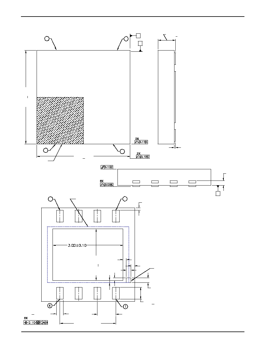
Min
Max
8L
0.1890(4.80)
0.1968(5.00)
Dimension D
Pkg
Min
Max
8L
0.355 (9.02)
0.400 (10.16)
0.149 (3.80)
0.1574 (4.00)
0.2284 (5.80)
0.2440 (6.20)
0.0532 (1.35)
0.0688 (1.75)
0.0040 (0.10)
0.0098 (0.25)
0.050 (1.27) BSC
0.013 (0.33)
0.020 (0.51)
0.0099 (0.25)
0.0196 (0.50)
0.0075 (0.19)
0.0098 (0.25)
0.016 (0.40)
0.050 (1.27)
0∞-8∞
X 45
∞
D
0.180 (4.57) MAX
0.015 (0.38)
--
0.100 (2.54)
BSC
0.014 (0.36)
0.022 (0.56)
D
0.245 (6.17)
0.295 (7.49)
0.045 (1.14)
0.060 (1.52)
0.110 (2.79)
0.150 (3.81)
0.120 (3.05)
0.150 (3.81)
0.300 (7.62)
0.325 (8.26)
0.310 (7.87)
0.380 (9.65)
CAT660
14
Doc. No. 5000, Rev. U
8-PAD TDFN (RD8, ZD8)
NOTE:
1. ALL DIMENSIONS ARE IN mm.
ANGLES IN DEGREES.
2. COPLANARITY APPLIES TO THE
EXPOSED PAD AS WELL AS
THE TERMINALS.
COPLANARITY SHALL NOT
EXCEED 0.08mm.
3. WARPAGE SHALL NOT
EXCEED 0.10mm.
4. PACKAGE LENGTH/PACKAGE
WIDTH ARE CONSIDERED AS
SPECIAL CHARACTERISTIC. (S)
0.75+0.05
A
B
5
8
4.00+0.10
(S)
1
PIN 1
INDEX AREA
4.00+0.10
(S)
4
0.0-0.05
0.20 REF.
C
5
DAP SIZE 3.5 X 2.4
8
0.10 MAX TYP.
0.15
0.15
0.20
0.10
2.20+0.10
0.10
0.80 TYP. (6x)
2.40 REF. (2x)
0.30+0.05 (8x)
0.50+0.10 (8x)
0.20
PIN 1 ID

CAT660
15
Doc. No. 5000, Rev. U
REVISION HISTORY
Date
Rev.
Reason
10/6/2003
R
Updated Typical Operating Characteristics data plots
10/7/2003
S
Updated Electrical Characteristics - Output Resistance
and Supply Current
Updated Typical Operating Characteristics data plots
10/15/2003
T
Updated Description - eliminated Commercial temp range
Updated ordering information - eliminated Commercial temp range
Updated operating ambient temperature ranges
1/20/2005
U
Changed ordering information for CAT660EXA to CAT660EVA
Changed ordering information for CAT660EXA-TE13 to CAT660EVA-TE13

CAT660
16
Doc. No. 5000, Rev. U
Catalyst Semiconductor, Inc.
Corporate Headquarters
1250 Borregas Avenue
Sunnyvale, CA 94089
Phone: 408.542.1000
Fax: 408.542.1200
www.catalyst-semiconductor.com
Publication #:
5000
Revison:
U
Issue date:
1/20/2005
Type:
Preliminary
Copyrights, Trademarks and Patents
Trademarks and registered trademarks of Catalyst Semiconductor include each of the following:
DPP TM
AE
2
TM
Catalyst Semiconductor has been issued U.S. and foreign patents and has patent applications pending that protect its products. For a complete list of patents
issued to Catalyst Semiconductor contact the Company's corporate office at 408.542.1000.
CATALYST SEMICONDUCTOR MAKES NO WARRANTY, REPRESENTATION OR GUARANTEE, EXPRESS OR IMPLIED, REGARDING THE SUITABILITY OF ITS
PRODUCTS FOR ANY PARTICULAR PURPOSE, NOR THAT THE USE OF ITS PRODUCTS WILL NOT INFRINGE ITS INTELLECTUAL PROPERTY RIGHTS OR THE
RIGHTS OF THIRD PARTIES WITH RESPECT TO ANY PARTICULAR USE OR APPLICATION AND SPECIFICALLY DISCLAIMS ANY AND ALL LIABILITY ARISING
OUT OF ANY SUCH USE OR APPLICATION, INCLUDING BUT NOT LIMITED TO, CONSEQUENTIAL OR INCIDENTAL DAMAGES.
Catalyst Semiconductor products are not designed, intended, or authorized for use as components in systems intended for surgical implant into the body, or
other applications intended to support or sustain life, or for any other application in which the failure of the Catalyst Semiconductor product could create a
situation where personal injury or death may occur.
Catalyst Semiconductor reserves the right to make changes to or discontinue any product or service described herein without notice. Products with data sheets
labeled "Advance Information" or "Preliminary" and other products described herein may not be in production or offered for sale.
Catalyst Semiconductor advises customers to obtain the current version of the relevant product information before placing orders. Circuit diagrams illustrate
typical semiconductor applications and may not be complete.