 | ÐлекÑÑоннÑй компоненÑ: CMPWR280 | СкаÑаÑÑ:  PDF PDF  ZIP ZIP |
Äîêóìåíòàöèÿ è îïèñàíèÿ www.docs.chipfind.ru
© 2000 Calirornia Micro Devices Corp. All rights reserved.
3/00
215 Topaz Street, Milpitas, California 95035 Tel: (408) 263-3214 Fax: (408) 263-7846 www.calmicro.com
CALIFORNIA MICRO DEVICES
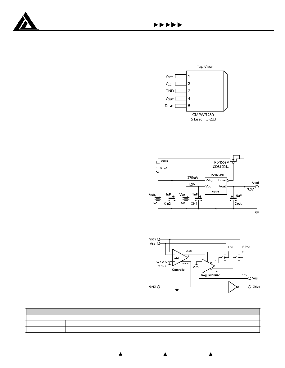
CMPWR280
1
Features
Automatic selection of V
CC
or V
SBY
Drive control signal for external V
AUX
switch
Continuous 3.3V output supply
Glitch-free output during supply transitions
Built-in hysteresis for supply selection
V
CC
regulates up to 1.5A output current
V
SBY
regulates up to 375mA output current
Foldback current limiting
Thermal shutdown with hysteresis
On-chip controller operates from V
CC
, V
SBY
or V
OUT
Applications
Peripheral Component Interface (PCI) Adapter Cards
Network Interface Cards (NICs)
Multiple Powered Systems
Systems with Standby Capabilities
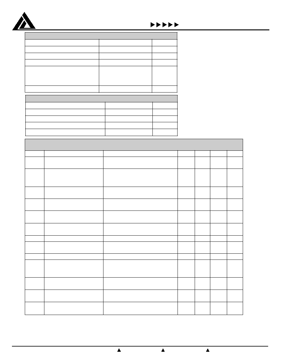
Product Description
The California Micro Devices SmartOR
TM
CMPWR280 is a fully
protected Dual-Input low dropout CMOS regulator that also
provides the necessary control signal for driving an external
auxiliary Pchannel MOSFET switch. The SmartOR
TM
device au-
tomatically selects one of three possible inputs on a priority
basis: V
CC
(1.5A), V
SBY
(375mA) or V
AUX
via the drive signal
used to control an external switch.
V
CC
is given first priority. In the event of the V
CC
supply being
powered down, the device will automatically deselect the V
CC
prior to regulator dropout and immediately select V
SBY
(second
priority) as its power source.
If neither V
CC
nor V
SBY
are present the drive control output will
turn-on an external P-channel MOSFET switch from an auxiliary
3.3V supply V
AUX
to V
OUT
.
All the necessary control circuitry needed to provide a smooth
and automatic transition between all three supplies has been
incorporated. This allows V
CC
to be dynamically switched with-
out loss of output voltage.
The CMPWR280 is internally protected against output
short-circuits, current overload and thermal overload.
CMPWR300 is a trademark of California Micro Devices Corp.
Pin Diagram
Typical Application Circuit
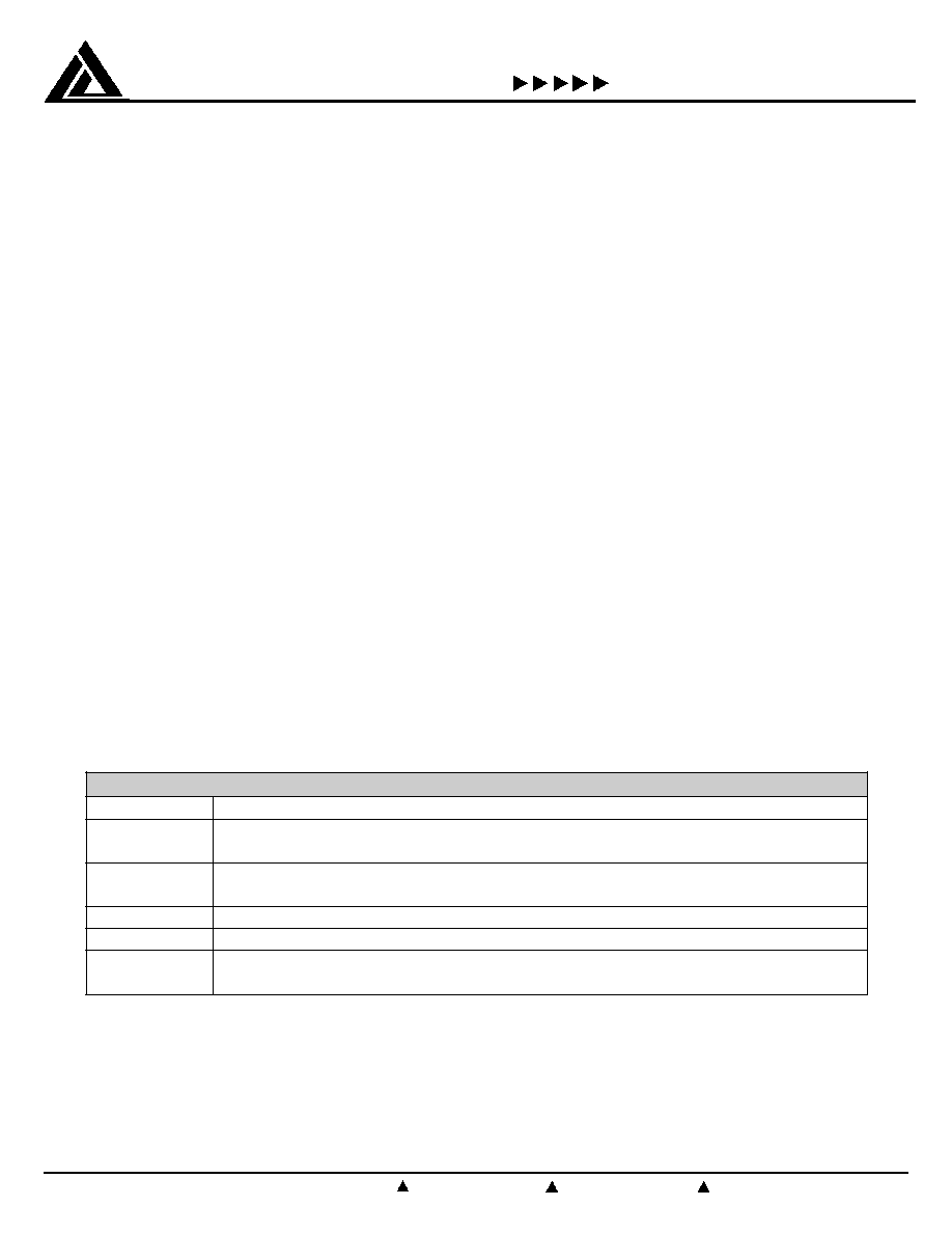
Simplified Electrical Schematic
When placing an order please specify desired shipping: Tubes or Tape & Reel.
1.5A SmartOR
TM
Dual Regulator with V
AUX
Drive
T
S
R
A
D
N
A
N
O
I
T
A
M
R
O
F
N
I
G
N
I
R
E
D
R
O
T
R
A
P
D
e
g
a
k
c
a
P
r
e
b
m
u
N
t
r
a
P
g
n
i
r
e
d
r
O
s
n
i
P
e
l
y
t
S
g
n
i
k
r
a
M
t
r
a
P
5
3
6
2
O
T
O
T
0
8
2
R
W
P
M
C
C0660200
CALIFORNIA MICRO DEVICES
©2000 California Micro Devices Corp. All rights reserved.
3/00
215 Topaz Street, Milpitas, California 95035 Tel: (408) 263-3214 Fax: (408) 263-7846 www.calmicro.com
CMPWR280
2
Note 1: The maximum power dissipation of this device is internally limited by thermal shutdown circuitry. To achieve a power dissipation of 3.0
watts, a case-to-ambient thermal resistance of 25°C/W must be provided. This will typically require dedicated heatsinking ability of the
printed circuit board. For more details, please see the Typical Thermal Characteristics section.
Note 2: The hysteresis defines the maximum level of acceptable disturbance on V
CC
during switching. It is recommended that the V
CC
source
impedance be kept below 0.15
to ensure the switching disturbance remains below the hysteresis during select/deselect transitions.
Note 3: Ground pin current consists of controller current (0.2mA) and regulator current when selected
S
G
N
I
T
A
R
M
U
M
I
X
A
M
E
T
U
L
O
S
B
A
r
e
t
e
m
a
r
a
P
g
n
i
t
a
R
t
i
n
U
)
M
B
H
(
n
o
it
c
e
t
o
r
P
D
S
E
0
0
0
2
V
V
C
C
, V
Y
B
S
V
,
T
U
O
5
.
0
-
d
n
G
,
0
.
6
+
V
e
g
a
tl
o
V
c
i
g
o
L
e
v
ir
D
V
C
C
(V
Y
B
S
5
.
0
-
D
N
G
,
5
.
0
+
)
V
e
g
n
a
R
e
r
u
t
a
r
e
p
m
e
T
e
g
a
r
o
t
S
0
5
1
+
o
t
0
4
-
t
n
e
i
b
m
A
g
n
it
a
r
e
p
O
0
7
+
o
t
0
o
C
n
o
it
c
n
u
J
g
n
it
a
r
e
p
O
0
5
1
+
o
t
0
)
3
6
2
-
O
T
(
:
n
o
it
a
p
is
si
D
r
e
w
o
P
1
e
t
o
N
d
e
ti
m
i
L
y
ll
a
n
r
e
t
n
I
W
S
N
O
I
T
I
D
N
O
C
G
N
I
T
A
R
E
P
O
r
e
t
e
m
a
r
a
P
e
g
n
a
R
t
i
n
U
V
,
C
C
V
Y
B
S
5
2
.
0
±
0
.
5
V
)t
n
e
i
b
m
A
(
e
r
u
t
a
r
e
p
m
e
T
0
7
+
o
t
0
o
C
t
n
e
rr
u
C
d
a
o
L
0
0
5
1
o
t
0
A
m
C
T
X
E
%
0
1
±
0
1
µF
S
C
I
T
S
I
R
E
T
C
A
R
A
H
C
G
N
I
T
A
R
E
P
O
L
A
C
I
R
T
C
E
L
E
)
e
s
i
w
r
e
h
t
o
d
e
i
f
i
c
e
p
s
s
s
e
l
n
u
s
n
o
i
t
i
d
n
o
c
g
n
i
t
a
r
e
p
o
r
e
v
o
(
l
o
b
m
y
S
r
e
t
e
m
a
r
a
P
s
n
o
i
t
i
d
n
o
C
N
I
M
P
Y
T
X
A
M
T
I
N
U
V
T
U
O
e
g
a
tl
o
V
t
u
p
t
u
O
r
o
t
a
l
u
g
e
R
I
<
A
m
0
D
A
O
L
V
(
A
m
0
0
5
1
<
C
C
)
5
3
1
.
3
0
3
.
3
5
6
4
.
3
V
I
<
A
m
0
D
A
O
L
V
(
A
m
5
7
3
<
Y
B
S
)
V
L
E
S
C
C
e
g
a
tl
o
V
t
c
e
l
e
S
V
C
C
d
e
l
b
a
n
E
r
o
t
a
l
u
g
e
R
0
5
.
4
0
7
.
4
V
S
E
D
C
C
V
C
C
e
g
a
tl
o
V
t
c
e
l
e
s
e
D
V
C
C
d
e
l
b
a
s
i
D
r
o
t
a
l
u
g
e
R
0
9
.
3
0
1
.
4
V
V
T
S
Y
H
C
C
e
g
a
tl
o
V
s
i
s
e
r
e
t
s
y
H
V
C
C
:
s
i
s
e
r
e
t
s
y
H
2
e
t
o
N
0
4
.
0
I
T
U
O
t
n
e
r
r
u
C
t
u
p
t
u
O
m
u
m
i
x
a
M
V
C
C
d
e
t
c
e
l
e
s
0
0
5
1
0
0
5
2
A
m
V
Y
B
S
d
e
t
c
e
l
e
s
5
7
3
0
5
7
I
C
/
S
t
n
e
r
r
u
C
t
u
p
t
u
O
ti
u
c
ri
C
t
r
o
h
S
V
C
C
d
e
t
c
e
l
e
s
0
0
8
A
m
V
Y
B
S
d
e
t
c
e
l
e
s
0
0
2
I
C
C
R
V
C
C
e
g
a
k
a
e
L
e
s
r
e
v
e
R
n
i
P
V
C
C
V
.
V
0
=
Y
B
S
V
5
=
0
1
0
0
1
µA
I
Y
B
S
R
V
Y
B
S
e
g
a
k
a
e
L
e
s
r
e
v
e
R
n
i
P
V
Y
B
S
0
=
.
V
V
C
C
V
5
=
0
1
0
1
V
D
A
O
L
R
V
C
C
n
o
it
a
l
u
g
e
R
d
a
o
L
V
C
C
I
,
d
e
t
c
e
l
e
s
D
A
O
L
A
m
0
0
5
1
o
t
A
m
5
1
=
0
3
V
m
V
Y
B
S
n
o
it
a
l
u
g
e
R
d
a
o
L
V
Y
B
S
I
,
d
e
t
c
e
l
e
s
D
A
O
L
A
m
5
7
3
o
t
A
m
5
=
0
3
V
E
N
IL
R
n
o
it
a
l
u
g
e
R
e
n
i
L
V
C
C
I
,
V
5
.
5
o
t
V
5
.
4
=
D
A
O
L
A
m
5
=
5
V
m
I
C
C
V
C
C
t
n
e
rr
u
C
y
l
p
p
u
S
V
C
C
I
,
d
e
t
c
e
l
e
s
T
U
O
A
m
0
=
5
.
1
0
.
3
A
m
V
S
E
D
C
C
V
>
C
C
V
>
X
U
A
V
r
o
T
U
O
1
.
0
2
.
0
I
Y
B
S
V
Y
B
S
t
n
e
rr
u
C
y
l
p
p
u
S
V
Y
B
S
I
,
d
e
t
c
e
l
e
s
T
U
O
A
m
0
=
5
.
1
0
.
3
A
m
I
D
N
G
:t
n
e
rr
u
C
d
n
u
o
r
G
3
e
t
o
N
V
y
l
n
o
(
d
e
l
b
a
si
D
r
o
t
a
l
u
g
e
R
T
U
O
)t
n
e
s
e
r
p
2
.
0
3
.
0
,
d
e
t
c
e
l
e
s
r
o
t
a
l
u
g
e
R
I
D
A
O
L
A
m
5
=
5
.
1
0
.
3
A
m
d
e
t
c
e
l
e
s
r
o
t
a
l
u
g
e
R
,
V
5
=
I
D
A
O
L
A
m
0
0
5
=
8
.
1
5
.
3
R
H
O
R
e
v
ir
D
S
D
h
g
i
H
R
S
D
V
o
t
C
C
V
,
C
C
V
>
L
E
S
C
C
5
0
1
k
R
H
O
R
e
v
ir
D
S
D
w
o
L
R
S
D
V
,
D
N
G
o
t
S
E
D
C
C
V
>
C
C
5
.
0
1
t
H
D
y
a
l
e
D
h
g
i
H
e
v
ir
D
C
E
V
I
R
D
V
,F
n
1
=
C
C
t
E
S
I
R
s
n
0
0
1
<
0
.
5
µs
t
L
D
y
a
l
e
D
w
o
L
e
v
ir
D
C
E
V
I
R
D
V
,F
n
1
=
C
C
t
L
L
A
F
s
n
0
0
1
<
5
.
0
T
E
L
B
A
S
I
D
e
r
u
t
a
r
e
p
m
e
t
n
w
o
d
t
u
h
S
5
6
1
°C
T
T
S
Y
H
si
s
e
r
e
t
s
y
h
l
a
m
r
e
h
T
0
3
© 2000 Calirornia Micro Devices Corp. All rights reserved.
3/00
215 Topaz Street, Milpitas, California 95035 Tel: (408) 263-3214 Fax: (408) 263-7846 www.calmicro.com
CALIFORNIA MICRO DEVICES
CMPWR280
3
Interface Signals
V
CC
is the primary 5V power supply for the internal regulator.
Whenever V
CC
exceeds V
CCSEL
(4.5V), the internal regulator
(1500mA) will be enabled and deliver a fixed 3.3V at V
OUT
.
When V
CC
falls below V
CCDES
(4.1V typically) the regulator
will be disabled.
Internal loading on this pin is typically 1.5mA when the
regulator is enabled, which reduces to 0.2mA whenever
the regulator is disabled. If V
CC
falls below either the V
SBY
or
V
OUT
voltage, the loading on V
CC
will reduce to only a few
microamperes.
During a V
CC
power up sequence, there will be an effective
step increase in V
CC
line current when the regulator is enabled.
The amplitude of this step increase will depend on the dc
load current and any current required for charging/
discharging the load capacitance. This line current transient
will cause a voltage disturbance at the V
CC
pin proportional
to the effective power supply source impedance being
delivered to the V
CC
input.
To prevent chatter during Select and Deselect transitions, a
built-in hysteresis voltage of 400mV has been incorporated.
It is recommended that the power supply connected to the
V
CC
input should have a source impedance of less than 0.15
to minimize the chatter during the enabling/disabling of
the regulator.
V
SBY
is the standby 5V supply power source, which is only
selected on when V
CC
< V
CCDES
. If V
SBY
is selected, the
regulator can deliver a maximum of 375mA load current.
Whenever V
SBY
exceeds both V
CC
and V
OUT
, it will be used to
provide all the internal bias currents and any necessary
regulator current.
GND is the reference for all voltages. The current that flows
in the ground connection is very low (typically 2.0mA) and
has minimal variation over all load conditions
V
OUT
is the regulator output voltage connection used to power
the load. An output capacitor of ten microfarads is used to
provide the necessary phase compensation, thereby preventing
oscillation. This capacitor also helps to minimize the peak
output disturbance during power supply changeover.
When both V
CC
and V
SBY
fall below V
OUT
, V
OUT
will be used to
provide the necessary quiescent current for the internal
reference circuits. This ensures excellent start-up characteristics
for the regulator.
Drive is an active LOW logic output intended to be used as
the control signal for driving an external P-channel MOSFET
switch whenever the regulator is disabled. This will allow the
voltage at V
OUT
to be powered from an auxiliary supply voltage
(3.3V).
The Drive pin is pulled HIGH to V
CC
whenever the regulator is
enabled, thus ensuring that the auxiliary supply remains isolated
during normal regulator operation.
s
n
o
i
t
c
n
u
F
n
i
P
l
o
b
m
y
S
n
o
i
t
p
i
r
c
s
e
D
V
Y
B
S
V
n
e
h
w
)
A
m
5
7
3
(
r
o
t
a
l
u
g
e
r
l
a
n
r
e
t
n
i
r
e
w
o
p
o
t
d
e
s
U
.t
u
p
n
i
y
l
p
p
u
S
V
5
e
v
it
is
o
P
y
b
d
n
a
t
S
C
C
t
o
n
si
.
e
l
b
a
li
a
v
a
V
C
C
V
r
e
v
e
n
e
h
w
)
A
5
.
1
(
r
o
t
a
l
u
g
e
r
l
a
n
r
e
t
n
i
e
h
t
s
r
e
w
o
P
.t
u
p
n
i
y
l
p
p
u
S
V
5
e
v
it
is
o
P
n
i
a
M
C
C
t
c
e
l
e
s
e
h
t
s
d
e
e
c
x
e
)
V
5
.
4
y
ll
a
c
i
p
y
t(
d
l
o
h
s
e
r
h
t
D
N
G
.
s
e
g
a
tl
o
v
ll
a
r
o
f
e
c
n
e
r
e
f
e
R
d
n
u
o
r
G
V
T
U
O
.)
V
3
.
3
(
e
g
a
tl
o
v
t
u
p
t
u
o
r
o
t
a
l
u
g
e
R
e
v
ir
D
l
a
n
r
e
t
n
i
e
h
t
r
e
v
e
n
e
h
w
t
u
p
t
u
o
W
O
L
e
v
it
c
A
.
h
c
ti
w
s
y
r
a
il
i
x
u
a
l
a
n
r
e
t
x
e
g
n
il
l
o
rt
n
o
c
r
o
f
l
a
n
g
is
c
i
g
o
L
.
d
e
l
b
a
si
d
si
r
o
t
a
l
u
g
e
r
CALIFORNIA MICRO DEVICES
©2000 California Micro Devices Corp. All rights reserved.
3/00
215 Topaz Street, Milpitas, California 95035 Tel: (408) 263-3214 Fax: (408) 263-7846 www.calmicro.com
CMPWR280
4
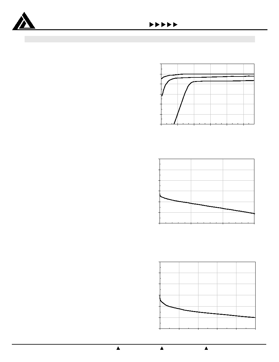
Fig 1.2. Vcc Load Regulation (pulse condition)
3.24
3.26
3.28
3.30
3.32
3.34
3.36
0
500
1000
1500
Load Current [mA]
Vo
u
t
[
V
]
Fig 1.3. Vsby Load Regul. (pulse condition)
3.24
3.26
3.28
3.30
3.32
3.34
3.36
0
100
200
300
400
500
Load Current [mA]
Vo
u
t
[
V
]
Typical DC Characteristics
Unless stated otherwise, all DC characteristics were measured at room temperature with a nominal V
CC
supply voltage of 5.0
volts and an output capacitance of 10µF.
Fig 1.1. V
CC
Line regulation
is measured while forcing the deselect threshold to an artificial
low level for loads of 100mA, 500mA and 1.5A. At the
maximum rated load of 1.5A, a drop in line regulation occurs
when the V
CC
supply voltage drops below 3.8V. For light
load conditions (100mA), regulation is maintained as low
as 3.2V.
Fig 1.2. V
CC
Load regulation (pulse condition)
performance is shown up to and beyond the rated load. A
change in load from 10% to 100% of rated current (150mA
to 1500mA) results in an output voltage change of about
20mV. This translates into an effective output impedance of
less than 15m.
Fig 1.3. V
SBY
Load regulation (pulse condition)
performance is shown up to and beyond the rated load. A
change in load from 10% to 100% of rated (50mA to 500mA)
results in an output voltage change of about 20mV. This
translates into an effective output impedance of less than
50m.
Fig 1.1. Line Regulation
3.05
3.10
3.15
3.20
3.25
3.30
3.35
3.3
3.6
3.9
4.2
4.5
4.8
Vcc [V]
V
out
[
V
]
100mA load
500mA load
1.5A load
© 2000 Calirornia Micro Devices Corp. All rights reserved.
3/00
215 Topaz Street, Milpitas, California 95035 Tel: (408) 263-3214 Fax: (408) 263-7846 www.calmicro.com
CALIFORNIA MICRO DEVICES
CMPWR280
5
Fig 1.4. Ground Current is shown across the entire
range of load conditions. The ground current of 2mA has
minimal variation across the range of load conditions and
shows only a slight increase at maximum load due to the
current limit protection circuitry.
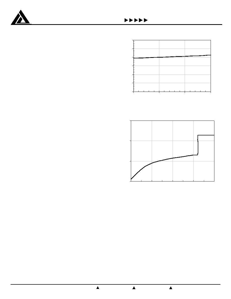
Fig 1.5. Supply Current of the device is shown across
the entire V
CC
range.
The supply current remains below 0.2mA when the V
CC
supply is lower than 4.2V and the regulator is deselected.
Above this point, the regulator is enabled and a supply
current of 2.0mA is conducted.
Fig 1.4. Ground Current
0.0
0.5
1.0
1.5
2.0
2.5
3.0
0
500
1000
1500
Load Current [mA]
I
GN
D
[m
A
]
Fig 1.5. Vcc Supply Current (No Load)
10
100
1000
10000
1
2
3
4
5
Vcc [V]
I
CC
[µ
A]