 | –≠–ª–µ–∫—Ç—Ä–æ–Ω–Ω—ã–π –∫–æ–º–ø–æ–Ω–µ–Ω—Ç: CM4072 | –°–∫–∞—á–∞—Ç—å:  PDF PDF  ZIP ZIP |

© 2005 California Micro Devices Corp. All rights reserved.
11/08/05
490 N. McCarthy Blvd., Milpitas, CA 95035-5112
Tel: 408.263.3214
Fax: 408.263.7846
www.cmd.com
1
CM4072
PRELIMINARY
Low Noise Charge Pump/Linear Regulator LED Driver
Features
∑
Low noise regulator with integrated charge pump
voltage-booster
∑
5V output with input voltage as low as 2.8V
∑
Charge pump can also power an external LDO
∑
Low noise in 20Hz to 20kHz audio band
∑
Up to 200mA continuous output current
∑
Low operating and shutdown currents
∑
Stable with low-ESR ceramic or tantalum capaci-
tors
∑
Over-current and over-temperature protection
∑
10-lead TDFN package, 3mm x 3mm
∑
Lead-free versions available
Applications
∑
White backlight LEDs for main display in wireless
handsets and LCD modules
∑
Power flash LEDs for camera phones
∑
3.3V to 5V conversion in PCMCIA cards, PCI
Express Cards, other applications needing 5V
∑
5V analog supply for audio codec in notebook
computers, PDAs, MP3 players, etc
Product Description
The CM4072 Low-noise Charge Pump / LDO Regulator is
designed to power white backlight LEDs used in main dis-
plays or camera flash LEDs in wireless handsets. The 5V
output provides up to 100mA continuous current for input
voltages from 3.0V to 5.5V, and up to 200mA for a nar-
rower range. This is accomplished with an integrated
charge pump that boosts the input voltage before feeding
it to an internal LDO linear regulator. The CM4072 oper-
ates with excellent power supply ripple rejection while
maintaining good power efficiency. The device utilizes two
external capacitors and operates at 250kHz. Separate
analog and digital ground pins are provided for the charge
pump and the rest of the circuitry to eliminate ground
noise feed-through from the charge pump to the regulated
output.
The CM4072 provides both overcurrent and thermal over-
load protection. Two enable inputs provide flexibility in
powering down the device. To maximize power saving in
shutdown mode, both enable inputs should be at a logic
low level. For applications that require the 5V output to be
re-established with minimum delay after shutdown, the
charge pump can be left enabled while the regulator is
disabled. The CMOS LDO regulator features low quies-
cent current even at full load, making it very suitable for
power sensitive applications.
A bypass pin is provided to further minimize noise by con-
necting an external capacitor between this pin and
ground.
The CM4072 is available in a 10-lead TDFN package,
with optional lead-free finishing, and is ideal for space crit-
ical applications
.
Typical Application
Simplified Block Diagram
CM4072
4
3
2
1
6
7
8
9
TDFN-10
5
10
V
IN
0.1
F*
C
S
2.2
F
+
+
C
BYP
C
P
+
PWM
*Optional
1
F
CHARGE PUMP
CS
CP-
CP+
C
P
C
S
V
CP
DGND
V
IN
EN_CP
EN_LDO
V
REF
LDO
BYP
GND
V
OUT
1
2
3
7
6
5
4
8
9
10
ENABLE CHARGE
PUMP
CONTROL
CIRCUIT
ENABLE LDO
0-200kHz

© 2005 California Micro Devices Corp. All rights reserved.
2
490 N. McCarthy Blvd., Milpitas, CA 95035-5112
Tel: 408.263.3214
Fax: 408.263.7846
www.cmd.com
11/08/05
CM4072
PRELIMINARY
PACKAGE / PINOUT DIAGRAM
Note: This drawing is not to scale.
CM4072-50DF/DE
10 Lead TDFN Package
CM407
GND
4
3
2
1
4
3
2
1
6
7
8
9
PAD
250xx
7
8
9
10
6
5
5
10
Pin 1
Marking
BOTTOM VIEW
(Pins Up View)
TOP VIEW
(Pins Down View)
PIN DESCRIPTIONS
LEAD(S)
NAME
DESCRIPTION
1
DGND
Ground for the charge pump circuit. This should be connected to the system (noisy) ground.
2
V
IN
Input power source for the device. Since the charge pump draws current in pulses at the
250kHz internal clock frequency, a low-ESR input decoupling capacitor is usually required close
to this pin to ensure low noise operation.
3
V
CP
Charge pump output which is connected to the external reservoir capacitor C
S
. This should be a
low-ESR capacitor. When the voltage on this pin reaches about 5.8V then the charge pump
pauses until the voltage on this pin drops to about 5.7V. This gives rise to at least 100mV of 'rip-
ple' (the frequency and amplitude of this ripple depends upon values of C
P
and C
S
and also the
ESR of C
S
).
4
GND
Ground reference for all internal circuits except the charge pump. This pin should be connected
to a "clean" low-noise analog ground
5
BYP
Bypass input connected to the internal voltage reference of the LDO regulator. An external
bypass capacitor C
BYP
of 0.1uF is recommended to minimize internal voltage reference noise
and maximize power supply ripple rejection.
6, 7
EN_LDO,
EN_CP
EN_LDO (pin 6) and EN_CP (pin 7) are active-high TTL-level logic inputs to enable the linear
regulator and charge pump according to the following truth table:
8
V
OUT
The regulated output. An output capacitor may be added to improve noise and load-transient
response. When the LDO regulator is disabled, an internal pull-down with a nominal resistance
of 50 ohms is activated to discharge the V
OUT
rail to GND
9, 10
CP+, CP-
CP+ (pin 9) and CP- (pin 10) are used to connect the external "flying" capacitor C
P
to the charge
pump. The charge stored in C
P
is transferred to the reservoir capacitor C
S
at the 250kHz inter-
nal clock rate.
EN_CP
(Pin 7)
EN_LDO
(Pin 6)
CHARGE PUMP
REGULATOR
1
1
Enabled
Enabled
1
0
Enabled
Disabled
0
1
Disabled
Disabled
0
0
Disabled
Disabled

© 2005 California Micro Devices Corp. All rights reserved.
11/08/05
490 N. McCarthy Blvd., Milpitas, CA 95035-5112
Tel: 408.263.3214
Fax: 408.263.7846
www.cmd.com
3
CM4072
PRELIMINARY
Ordering Information
Note 1: Parts are shipped in Tape & Reel form unless otherwise specified.
Specifications
PART NUMBERING INFORMATION
Leads
Package
Standard Finish
Lead-free Finish
Ordering Part
Number
1
Part Marking
Ordering Part
Number
1
Part Marking
10
TDFN-10
CM4072-50DF
CM407 250DF
CM4072-50DE
CM407 250DE
ABSOLUTE MAXIMUM RATINGS
PARAMETER
RATING
UNITS
ESD Protection (HBM)
±
2000
V
V
EN
Logic Input Voltage
(V
IN
+ 0.5) to (GND - 0.5)
V
V
IN,
V
OUT
Pin Voltages
+5.5 to (GND - 0.5)
V
Storage Temperature Range
-65 to +150
∞C
Operating Temperature Range
Ambient
Junction
-40 to +85
-40 to +150
∞C
∞C
STANDARD OPERATING CONDITIONS
PARAMETER
VALUE
UNITS
Input Voltage Range (V
IN
)
2.8 to 5.5
V
Ambient Operating Temperature
-40 to +85
∞C
JA
of TDFN package on PCB
200 (approx.)
∞C/W
Output Load Current (I
OUT
)
0 to 200
mA
C
BYP
0.1
F
C
OUT
0 to 100
F
RECOMMENDED EXTERNAL COMPONENTS
DEVICE
VALUE
UNITS
C
S
2.2
F
C
P
1.0
F

© 2005 California Micro Devices Corp. All rights reserved.
4
490 N. McCarthy Blvd., Milpitas, CA 95035-5112
Tel: 408.263.3214
Fax: 408.263.7846
www.cmd.com
11/08/05
CM4072
PRELIMINARY
Specifications (cont'd)
Note 1: Unless otherwise noted, electrical operating characteristics are specified with T
A
= 0 to 70∞C, V
IN
= 5.0V, I
OUT
=100mA,
C
OUT
=10
F, C
P
= 1
F, C
S
= 10
F.
Note 2: These parameters are guaranteed by design and characterization.
ELECTRICAL OPERATING CHARACTERISTICS
(SEE NOTE 1)
SYMBOL
PARAMETER
CONDITIONS
MIN
TYP
MAX
UNITS
V
CP
Charge Pump Output Voltage
V
OUT
= 5V, 1mA < I
OUT
< 100mA
5.5
5.8
7
V
V
OUT
Regulator Output Voltage
V
IN
= 4.0V, 1mA < I
OUT
< 100mA
4.85
5.15
V
V
R LOAD
Load Regulation
I
OUT
= 1mA to 100mA
0.2
%
V
R LINE
Line Regulation
Vary V
IN
from 3.0V to 5.0V
0.02
%
R
DISCHG
V
OUT
Discharge Resistance
LDO regulator disabled, EN_LDO
grounded, V
IN
= 5V
500
I
GND
LDO Regulator Ground Current via
the GND pin
Shutdown (EN_LDO grounded)
1
10
A
Regulator Enabled, I
OUT
= 0mA
180
A
Regulator Enabled, I
OUT
= 100mA
180
A
I
DGND
Charge Pump Shutdown Current
via DGND pin
EN_CP grounded, V
IN
= 5V
1
10
A
PSRR
Power Supply Ripple Rejection
I
OUT
= 100mA, C
BYP
=0.1
F, Note 2
f = 100Hz
f = 10kHz
42
42
dB
dB
e
NO
Output Voltage Noise
BW=22Hz-22kHz, C
OUT
= 10
F,
C
BYP
= 0.1
F, I
OUT
= 100mA, Note 2
35
Vrms
BW=22Hz-22kHz, C
P
= 1
F, C
S
=3
F,
C
OUT
= C
BYP
= 0.1
F, I
OUT
= 100mA,
Note 2
38
Vrms
V
IH
EN_CP, EN_LDO Input High
Threshold
V
IN
= 5.0V
2.0
V
V
IL
EN_CP, EN_LDO Input Low
Threshold
V
IN
= 5.0V
0.5
V
I
LIM
Overload Current Limit
LDO Only, Note 2
200
300
mA
I
SC
Output Short Circuit Current
LDO Only, Note 2
50
mA
T
JSD
Thermal Shutdown Junction
Temperature
170
∞C
T
HYS
Thermal Shutdown Hysteresis
25
∞C

© 2005 California Micro Devices Corp. All rights reserved.
11/08/05
490 N. McCarthy Blvd., Milpitas, CA 95035-5112
Tel: 408.263.3214
Fax: 408.263.7846
www.cmd.com
5
CM4072
PRELIMINARY
Performance Information
Figure 1. CM4072 Noise Spectrum ( T
A
= 25∞C, C
P
=0.47
F, C
S
= 1.5
F,
C
OUT
= 10
F, C
BYP
= 0.1
F, I
OUT
=100mA )
Figure 2. CM4072 PSRR (upper curve with V
IN
= 3.3V, lower curve
with V
IN
= 5V, I
OUT
= 100mA both cases)
p
1.00E-08
1.00E-07
1.00E-06
1.00E-05
1.00E-04
1.00E-03
10
100
1000
10000
100000
Frequency [Hz]
Vo
l
t
a
g
e
[
V]
noise floor
Cs=1.5uF
Note: Noise peaks may appear for different values of C
P
, C
S
& I
OUT
, and are due to the ripple frequency of the charge pump (see later).
0.0
10.0
20.0
30.0
40.0
50.0
60.0
70.0
10
100
1000
10000
100000
Frequency [Hz]
PSR
R
[
d
B
]
Measured by forcing V
IN
voltage to 3.3V & 5.0V dc, then sweeping 100mV ac on V
IN
. C
OUT
= 10
F, C
BYP
= 0.1
F.

© 2005 California Micro Devices Corp. All rights reserved.
6
490 N. McCarthy Blvd., Milpitas, CA 95035-5112
Tel: 408.263.3214
Fax: 408.263.7846
www.cmd.com
11/08/05
CM4072
PRELIMINARY
Performance Information (cont'd)
Typical DC Characteristics
(T
A
=25∞C, C
P
=1.0
F, C
S
=10
F, C
BYP
=0.1
F, C
OUT
=10
F unless otherwise noted)
Figure 3. V
OUT
vs. I
OUT
(V
IN
= 5V)
Figure 4. V
OUT
vs. V
IN
Figure 5. CS Pin vs. V
IN
Figure 6. Dropout Voltage (LDO Only)
Figure 7. V
EN
Threshold vs. V
IN
Figure 8. I
IN
vs. V
IN
Figure 9. I
IN
vs. I
OUT
Figure 10. Overcurrent Characteristic (LDO only)
4.9
4.92
4.94
4.96
4.98
5
5.02
5.04
5.06
5.08
5.1
0
20
40
60
80
100
I
OUT
[mA]
V
OU
T
[V
]
4.9
4.92
4.94
4.96
4.98
5
5.02
5.04
5.06
5.08
5.1
3
3.5
4
4.5
5
5.5
V
IN
[V]
V
OU
T
[V
]
I
OUT
= 0mA
I
OUT
= 100mA
5
5.25
5.5
5.75
6
6.25
6.5
6.75
7
3
3.5
4
4.5
5
5.5
V
IN
[V]
V
CP
[V
]
at T=150'C, T=85'C and T=25'C
0
100
200
300
400
0
10
20
30
40
50
60
70
80
90 100
I
OUT
[mA]
T
A
=150∞
C
T
A
=25∞
C
T
A
=85∞C
V
DO
[mV]
1
1.1
1.2
1.3
1.4
1.5
1.6
1.7
1.8
1.9
2
3
3.5
4
4.5
5
5.5
V
IN
[V]
V
EN
[V]
0
50
100
150
200
250
300
3
3.5
4
4.5
5
5.5
V
IN
[V]
I
IN
[
A]
0
50
100
150
200
250
0
20
40
60
80
100
I
OUT
[mA]
I
IN
[
mA]
V_IN=3.1V
V_IN=5V
0
1
2
3
4
5
6
0
0.1
0.2
0.3
0.4
0.5
I
OUT
[A]
V
OU
T
[V
]
© 2005 California Micro Devices Corp. All rights reserved.
11/08/05
490 N. McCarthy Blvd., Milpitas, CA 95035-5112
Tel: 408.263.3214
Fax: 408.263.7846
www.cmd.com
7
CM4072
PRELIMINARY
Performance Information (cont'd)
Transient Characteristics
(T
A
=25∞C, C
P
=1.0
F, C
S
=10
F, C
BYP
=0.1
F, C
OUT
=10
F unless otherwise noted)
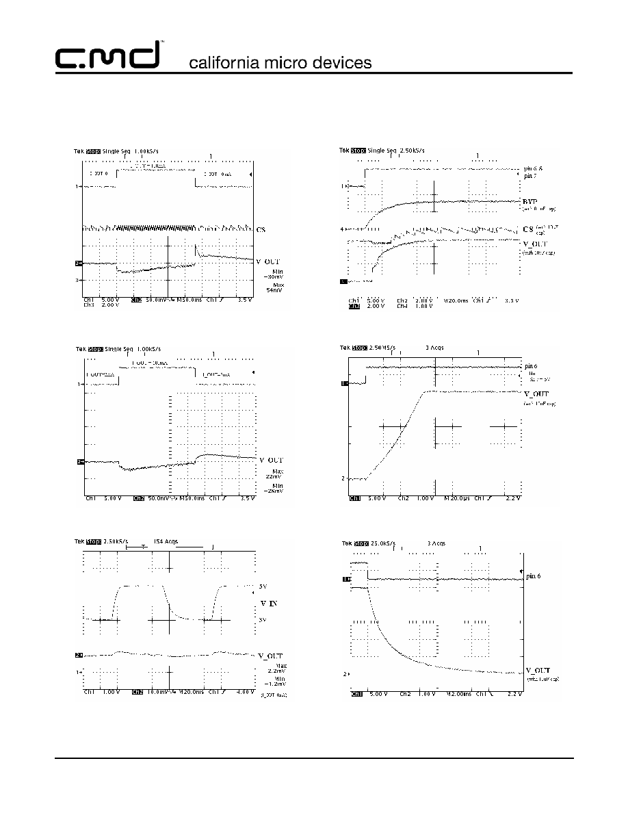
Figure 11. Load Regulation (0mA to 100mA)
Figure 12. Load Regulation (2mA to 100mA)
Figure 13. Line Regulation
Figure 14. Cold Start / Power-Up
Figure 15. LDO Power-Up
Figure 16. LDO Power-Down

© 2005 California Micro Devices Corp. All rights reserved.
8
490 N. McCarthy Blvd., Milpitas, CA 95035-5112
Tel: 408.263.3214
Fax: 408.263.7846
www.cmd.com
11/08/05
CM4072
PRELIMINARY
Performance Information (cont'd)
Transient Characteristics
(T
A
=25∞C, V
IN
=5V, C
P
=1.0
F, C
S
=10
F, C
BYP
=0.1
F, C
OUT
=10
F unless otherwise noted)
Figure 17. V
OUT
with V
IN
= 5V
Figure 18. V
OUT
with V
IN
=3.0V, I
OUT
=100mA
Figure 19. Bypass Pin Voltage
Figure 20. I
IN
Leakage Current (Pins 6,7=0V)
Figure 21. Undervoltage Lockout
4.90
4.95
5.00
5.05
5.10
-50
-25
0
25
50
75
100
125
150
Temperature [∞C]
V
OUT
[V]
I_OUT=0
I_OUT=30mA
I_OUT=75mA
I_OUT=100mA
I_OUT=150mA
4.8
4.85
4.9
4.95
5
5.05
5.1
-50
-25
0
25
50
75
100
125
Temperature [∞C]
V
OU
T
[V]
1.6
1.605
1.61
1.615
1.62
1.625
1.63
1.635
1.64
1.645
1.65
-50
-25
0
25
50
75
100
125
150
Temperature [∞C]
V
BYP
[V]
0
0.5
1
1.5
2
2.5
3
3.5
4
4.5
5
-50
-25
0
25
50
75
100
125
150
Temperature [∞C]
Cu
rren
t
[
A]
0
0.5
1
1.5
2
2.5
3
-50
-25
0
25
50
75
100
125
150
Temperature ['C]
V_
I
N
Vo
l
t
a
g
e
[V]
© 2005 California Micro Devices Corp. All rights reserved.
11/08/05
490 N. McCarthy Blvd., Milpitas, CA 95035-5112
Tel: 408.263.3214
Fax: 408.263.7846
www.cmd.com
9
CM4072
PRELIMINARY
Application Information
Ripple Frequency
The charge pump internal oscillation frequency is
about 250kHz. However, this is the continuous, free-
running frequency, which is usually only seen while the
charge pump is powering up. Such a sawtooth 'ripple'
waveform on CS can have a much lower frequency
than 250kHz. This mode of operation is necessary to
conserve power. If it were not done this way, then a
much larger package with heatsink would be required.
The frequency of this 'ripple' is affected by V
IN
, I
OUT
,
C
S
capacitor value and C
P
capacitor value.
Guidelines for External Capacitors
(1) To find C
P
: specify value of V
IN
, and highest value
of I
OUT
:
If V
IN
= 3.3V +/- 5%, then minimum value
of C
P
(µF) = I
OUT
(mA) / 85.
If V
IN
= 5.0V +/- 10%, then minimum value
of C
P
(µF) = I
OUT
(mA) / 700
(2) The V
IN
decoupling capacitor, C
IN
, should typically
be much greater than C
P
to prevent voltage droop dur-
ing C
P
charging. Excessive glitches on V
IN
will affect
the output voltage V
OUT
. C
IN
is typically 10X greater
than C
P
.
(3) C
S
should be small to ensure that the ripple fre-
quency is high, but at least 2x greater than C
P
, other-
wise the ripple amplitude will be very high. Reducing
the value of C
S
will increase the ripple frequency.
Examples of C
S
ripple frequencies (C
S
=10
F,
T
A
=25∞C) are shown in following tables:
(4) C
OUT
, the optional V
OUT
capacitor, helps minimize
noise and improve load regulation; 0.1µF to 100µF is
recommended.
(5) C
BYP
, the optional bypass capacitor helps reduce
noise in the LDO; 0.1µF is recommended.
After choosing external component values, check in-
system performance (at min/max V
IN
, max tempera-
ture, and min/max I
OUT
). See the troubleshooting guide
on next page for tips if there are problems.
Charge Pump Noise
The charge pump is 'digital' in operation and can pro-
duce digital noise at both the free-running frequency
and at the ripple frequency.
To minimize noise, PCB grounding is important! This
part requires short, low-impedance ground connec-
tions for DGND (pin 1), GND (pin 4), the V
IN
decou-
pling capacitor (pin 2), the C
S
capacitor (pin 3), the
Bypass decoupling capacitor (pin 5) and the V
OUT
decoupling capacitor (pin 8). All decoupling capacitors
and the C
S
capacitor should be low-ESR ceramics.
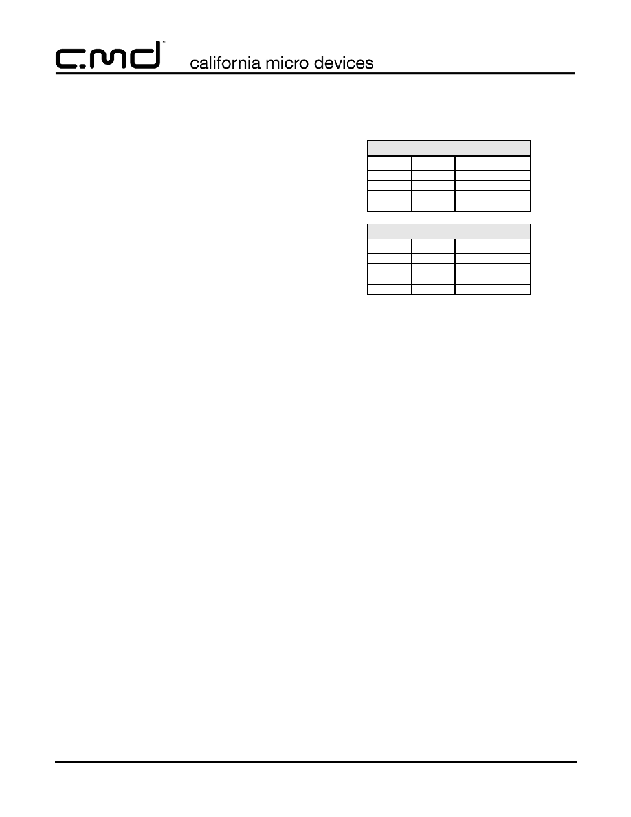
The C
P
capacitor needs to be low-ESR.
C
P
= 0.47
F
V
IN
I
OUT
C
S
Frequency
3.14
15mA
46kHz
3.60
15mA
35kHz
4.50
70mA
76kHz
5.50
70mA
56kHz
C
P
= 1.0
F
V
IN
I
OUT
C
S
Frequency
3.14
100mA
250kHz
3.60
100mA
110kHz
4.50
100mA
67kHz
5.50
100mA
49kHz

© 2005 California Micro Devices Corp. All rights reserved.
10
490 N. McCarthy Blvd., Milpitas, CA 95035-5112
Tel: 408.263.3214
Fax: 408.263.7846
www.cmd.com
11/08/05
CM4072
PRELIMINARY
Efficiency
The power efficiency in % of the combined charge
pump and LDO is approximately:
100 x (V
OUT
) / (V
IN
x 2)
Power Dissipation
The dissipation of the part is approximately:
((V
IN
x 2) - V
OUT
) x I
OUT
The TDFN-10 package heats at a rate of about 200∞C/
W (
JA
). Note that this value is approximate because it
depends upon the copper tracks and ground planes on
the pcb. If V
IN
= 5V and I
OUT
= 100mA then the power
dissipation will be approximately 500mW. Multiplying
this by the
JA
gives an internal temperature about
100∞C higher than the ambient temperature (T
A
). If the
T
A
is 70∞C then the internal temperature will be
approximately 170∞C which will trigger the overtemper-
ature circuit and lead to power-down.
Internal temperature = Ambient temperature
+ (
JA
x Power dissipation )
(Must be less than 170∞C)
Note that the evaluation PCB has a
JA
of less than
150∞C/W, based upon measured performance.
How to Reduce the Power Dissipation of the Part
and How to Get More Than 100mA
If V
IN
= 5V typ., then the charge pump / LDO combina-
tion is capable of providing more than 100mA. The only
problem is power dissipation.
If the input voltage is lowered using an external diode
then the output current can be increased without caus-
ing the part to overheat. The circuit below illustrates an
example of how to increase the output current.
Using this circuit, I
OUT
can be 200mA if V
IN
= 4.75V,
and yet the part will not overheat even if V
IN
= 5.25V,
I
OUT
=200mA and the ambient temperature is 85∞C.
Warnings
The charge pump output V
CP
(pin 3) must not be
shorted to GND or held below its internally-set voltage
while the part is powered. This usually results in the
destruction of the part.
With V
IN
= 5V, the maximum current that can be con-
tinuously drawn from V
CP
is approximately 100mA dc.
Never short C
P
+ (pin 9) to C
P
- (pin 10). This will cause
large currents to flow from V
IN
to DGND through the
part, usually causing its destruction. This will happen
even if EN_CP and EN_LDO are off.
Troubleshooting Guide
1) Is the output voltage drooping under heavy loads?
Perhaps the charge pump cannot provide the neces-
sary current. Try increasing the value of C
P
. If that
does not work, then, is V
IN
too low? Is V
IN
dropping
during the C
P
charging cycle? If V
IN
is not suitably
decoupled and drops below 3.1V then the available
current will be very low.
2) Is the output voltage oscillating between 5V and 0V?
The part may be reaching its overtemperature limit.
Reduce current consumption, reduce
JA
or add an
external diode on the input to reduce V
IN
.
3. Is the part too noisy? Try increasing the value (or
reducing ESR) of C
S
, C
IN
, C
S
, C
B
. At minimum current
the charge pump ripple frequency will be low. If V
OUT
noise is at the charge pump ripple frequency, then
change values of C
P
and C
S
. Reducing the input volt-
age V
IN
will reduce the charge pump ripple frequency
noise on V
OUT
.
4. Will the part power up? Pin 6 must be HIGH to
power up. Even if pin 7 is HIGH, pin 6 must also be
high to power up.
5. Can the cold start power-up time be reduced? Yes,
by reducing the value of the C
BYP
.
CM4072
4
3
2
1
6
7
8
9
TDFN-10
5
10
5V
C
i
10
F
C
S
3
F
+
+
C
BYP
0.1
F
+
V
OUT
C
O
0.1
F
+
C
P
+
Enable
1
F
±
10%
1N4006

© 2005 California Micro Devices Corp. All rights reserved.
11/08/05
490 N. McCarthy Blvd., Milpitas, CA 95035-5112
Tel: 408.263.3214
Fax: 408.263.7846
www.cmd.com
11
CM4072
PRELIMINARY
Mechanical Details
TDFN-10 Mechanical Specifications
Dimensions for the CM4072-50DF/DE supplied in a
10-lead TDFN package are presented below.
For complete information on the TDFN-10, see the Cal-
ifornia Micro Devices TDFN Package Information doc-
ument.
This package is compliant with JEDEC standard MO-229, variation
WEED-3 with exception of the "D2" and "E2" dimensions as called
out in the table above.
Package Dimensions for 10-Lead TDFN
PACKAGE DIMENSIONS
Package
TDFN
JEDEC
No.
MO-229 (Var. WEED-3)
Leads
10
Dim.
Millimeters
Inches
Min
Nom
Max
Min
Nom
Max
A
0.70
0.75
0.80
0.028 0.030 0.031
A1
0.00
0.02
0.05
0.000 0.001 0.002
A2
0.45
0.55
0.65
0.018 0.022 0.026
A3
0.20
0.008
b
0.18
0.25
0.30
0.007 0.010 0.012
D
3.00
0.118
D2
2.20
2.30
2.40
0.087 0.091 0.094
E
3.00
0.118
E2
1.40
1.50
1.60
0.055 0.060 0.063
e
0.50
0.020
K
0.20
0.008
L
0.20
0.30
0.40
0.008 0.012 0.016
# per
tape and
reel
3000 pieces
Controlling dimension: millimeters
Mechanical Package Diagrams
BOTTOM VIEW
A A3
A1
0.10 C
0.08 C
SIDE VIEW
TOP VIEW
b
L
0.10
C A B
M
8X
D2
E2
e
GND PAD
D
E
Pin 1
Marking
4
3
2
1
7
8
9
10
A2
K
7
8
9
10
3
2
1
4
5
6
5
6
Pin 1 ID
C0.35