 | ÐлекÑÑоннÑй компоненÑ: CM1410 | СкаÑаÑÑ:  PDF PDF  ZIP ZIP |
Äîêóìåíòàöèÿ è îïèñàíèÿ www.docs.chipfind.ru
©
2005 California Micro Devices Corp. All rights reserved.
09/15/05
490 N. McCarthy Blvd., Milpitas, CA 95035-5112
Tel: 408.263.3214
Fax: 408.263.7846
www.calmicro.com
1
CM1410
4 Channel Headset EMI Filter with ESD Protection
Features
·
Functionally and pin compatible with CSPEMI200A
device
·
Pi-style EMI filters in a capacitor-resistor-capacitor
(C-R-C) network
·
Four channels of EMI filtering with ESD protection
·
Includes 1 channel of ESD-only protection
·
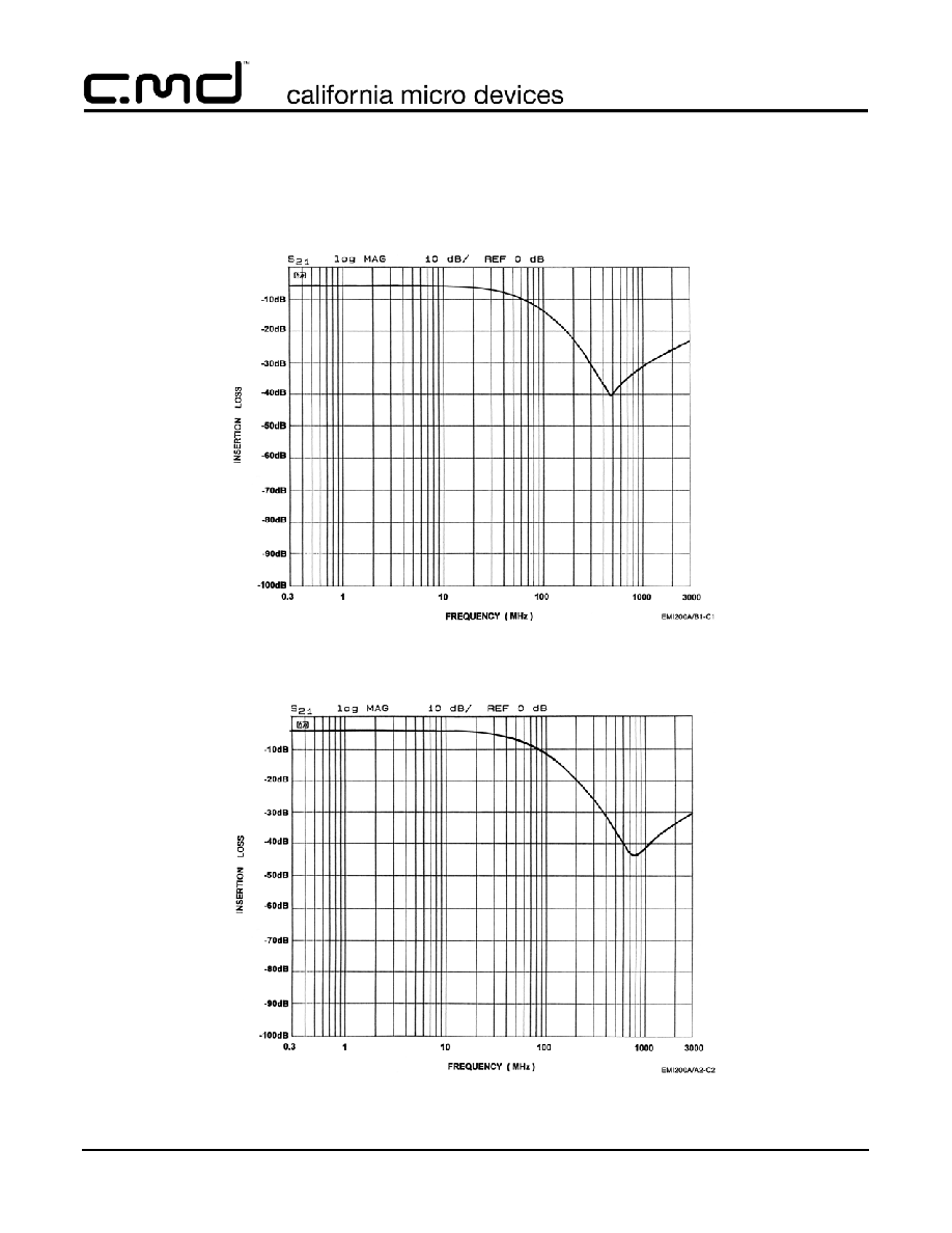
Greater than 30dB attenuation at 1GHz
·
+
8kV ESD protection on each channel
(IEC 61000-4-2 Level 4, contact discharge)
·
+
15kV ESD protection on each channel (HBM)
·
Supports bipolar signals--ideal for
audio applications
·
Chip Scale Package features extremely low
lead inductance for optimum filter and ESD
performance
·
11-bump, 2.046mm X 1.436mm footprint
Chip Scale Package (CSP)
·
Optiguard
TM
coated for improved reliability at
assembly
·
Lead-free version available
Applications
·
EMI filtering and ESD protection for audio ports
·
Wireless Handsets
·
Handheld PCs / PDAs
·
MP3 Players
·
Digital Camcorders
·
Notebooks
·
Desktop PCs
Product Description
The CM1410 is a quad low-pass filter array integrating
four pi-style filters (C-R-C) that reduce EMI/RFI emis-
sions while at the same time providing ESD protection.
This device is custom-designed to interface with the
headset port on a cellular telephone, and contains 3
different filter values. Each high quality filter provides
more than 20dB attenuation in the 800-2700 MHz
range. These pi-style filters support bidirectional filter-
ing, controlling EMI both to and from the microphone
and speaker elements. They also support bipolar sig-
nals, enabling audio signals to pass through without
distortion.
In addition, the CM1410 provides a very high level of
protection for sensitive electronic components that may
be subject to electrostatic discharge (ESD). The
CM1410 can safely dissipate ESD strikes of
+
8kV, the
maximum requirement of the IEC 61000-4-2 interna-
tional standard. Using the MIL-STD-883 (Method 3015)
specification for Human Body Model (HBM) ESD, the
device provides protection for contact discharges to
greater than
+
15kV. The CM1410 also includes a sin-
gle channel of ESD-only protection.
The CM1410 is particularly well suited for portable
electronics (e.g., cellular telephones, PDAs, notebook
computers) because of its small package format and
low weight.
The CM1410 incorporates Optiguard
TM
coating which
results in improved reliability at assembly.The CM1410
is available in a space-saving, low-profile Chip Scale
Package with optional lead-free finishing.
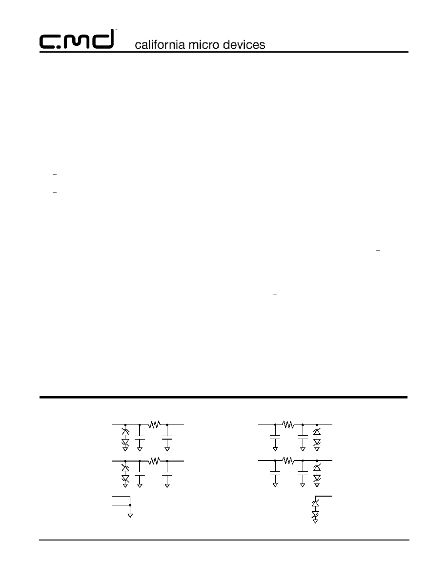
Electrical Schematic
10
100pF
100pF
100
47p
F
47p
F
MIC_IN1
B2
A2
A3
A4
B4
C1
C2
C3
C4
B3
ESD1
MIC_IN2
SPKR_OUT1
SPKR_OUT2
GND
GND
SPKR_IN2
SPKR_IN1
MIC_OUT2
MIC_OUT1
B1
68
47pF
47pF
10
100pF
100pF
©
2005 California Micro Devices Corp. All rights reserved.
2
490 N. McCarthy Blvd., Milpitas, CA 95035-5112
Tel: 408.263.3214
Fax: 408.263.7846
www.calmicro.com
09/15/05
CM1410
Ordering Information
Note 1: Parts are shipped in Tape & Reel form unless otherwise specified.
Note 2: Lead-free devices are specified by using a "
+
" character for the top side orientation mark.
PIN DESCRIPTIONS
PIN
NAME
DESCRIPTION
A1
N.B.
No Bump used for orientation / alignment
A2
MIC_IN2
Microphone Input 2 (from microphone)
A3
SPKR_OUT1
Speaker Output 1 (to speaker)
A4
SPKR_OUT2
Speaker Output 2 (to speaker)
B1
MIC_IN1
Microphone Input 1 (from microphone)
B2
ESD1
ESD Protection Input. Provides a channel specifically for ESD protection purposes.
B3
GND
Device Ground
B4
GND
Device Ground
C1
MIC_OUT1
Microphone Output 1 (to audio circuitry)
C2
MIC_OUT2
Microphone Output 2 (to audio circuitry)
C3
SPKR_IN1
Speaker Input 1 (from audio circuitry)
C4
SPKR_IN2
Speaker Input 2 (from audio circuitry)
N103
4
3
2
1
C
B
A
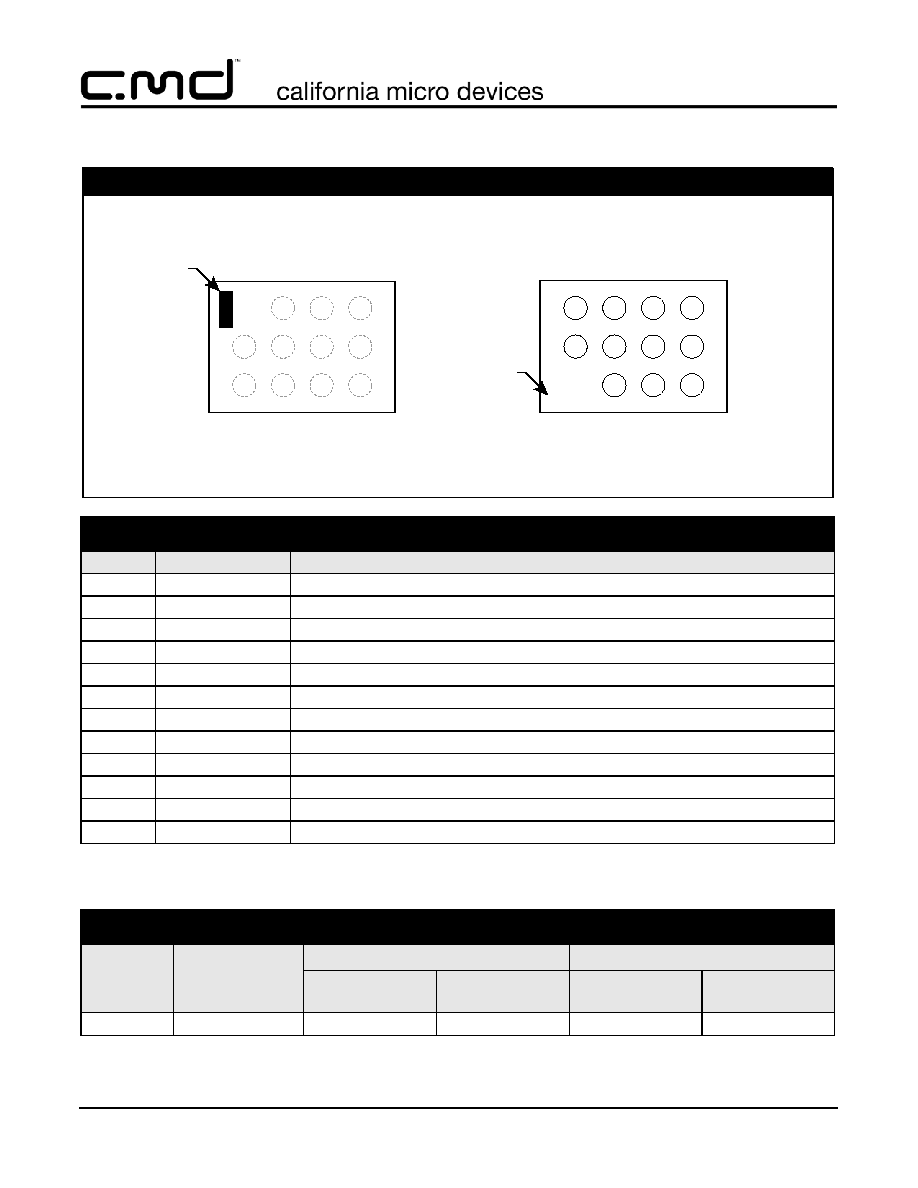
Orientation
Marking
(see note 2)
MIC_IN2
MIC_IN1
SPKR_OUT1 SPKR_OUT2
ESD1
GND
GND
MIC_OUT1 MIC_OUT2 SPKR_IN1 SPKR_IN2
A3
A2
Orientation
Marking
A4
B4
B3
B2
B1
C4
C3
C2
C1
A1
PACKAGE / PINOUT DIAGRAMS
Notes:
TOP VIEW
CM1410
CSP Package
BOTTOM VIEW
(Bumps Down View)
(Bumps Up View)
2) Lead-free devices are specified by using a "
+
" character for the top side orientation mark.
1) These drawings are not to scale.
PART NUMBERING INFORMATION
Bumps
Package
Standard Finish
Lead-free Finish
2
Ordering Part
Number
1
Part Marking
Ordering Part
Number
1
Part Marking
11
CSP
CM1410-03CS
N103
CM1410-03CP
N103
©
2005 California Micro Devices Corp. All rights reserved.
09/15/05
490 N. McCarthy Blvd., Milpitas, CA 95035-5112
Tel: 408.263.3214
Fax: 408.263.7846
www.calmicro.com
3
CM1410
Specifications
Note 1: T
A
=25
°
C unless otherwise specified.
Note 2: ESD applied to input pins with respect to GND, one at a time, pins A2, A3, A4, B1 and B2 only.
Note 3: Clamping voltage is measured at the opposite side of the EMI filter to the ESD pin. For example, if ESD is applied to Pin B1,
then clamping voltage is measured at Pin C1.
Note 4: Unused pins are left open
Note 5: The parameters are guaranteed by design and characterization.
Note 6: Z
SOURCE
=50
, Z
LOAD
=50
.
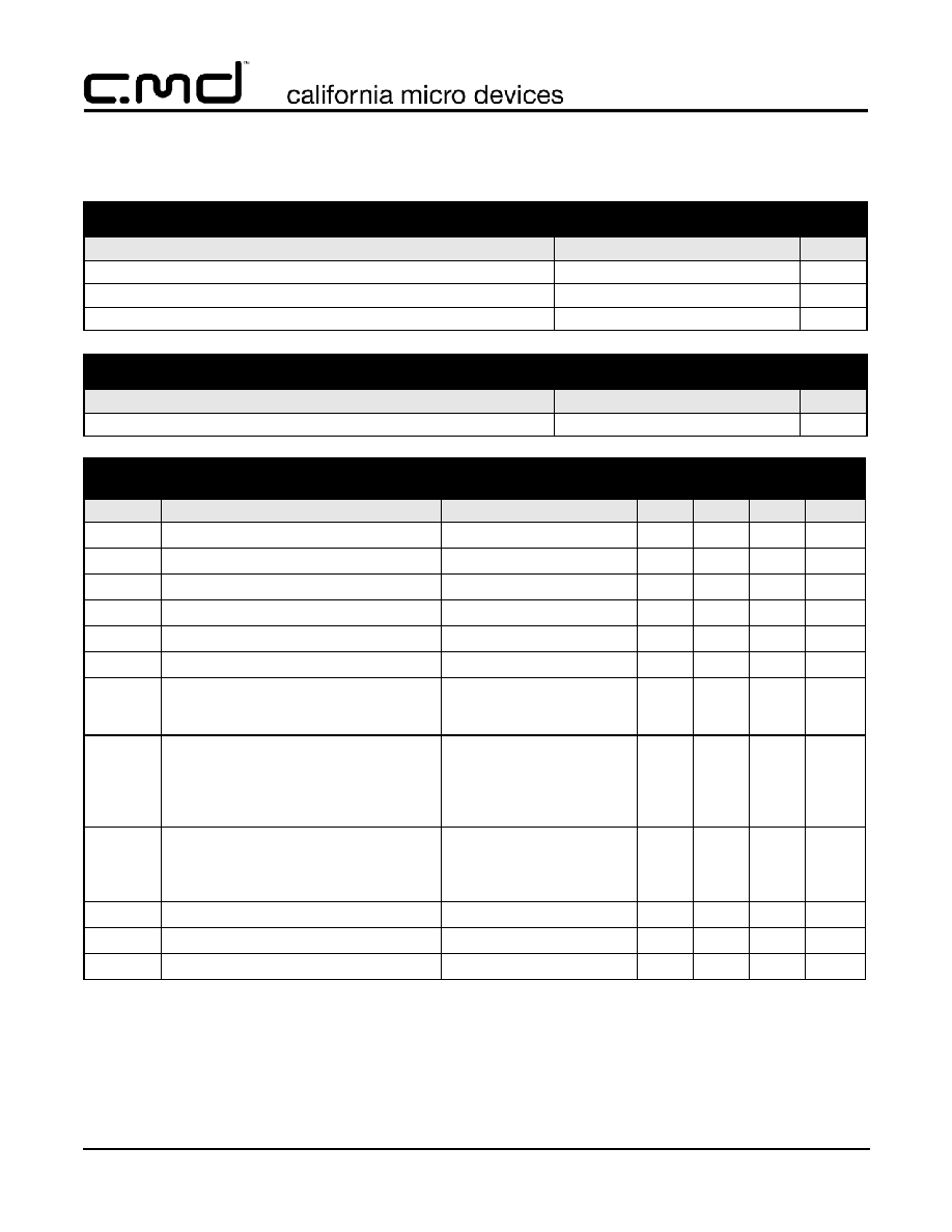
ABSOLUTE MAXIMUM RATINGS
PARAMETER
RATING
UNITS
Storage Temperature Range
-65 to +150
°C
DC Power per Resistor
100
mW
DC Package Power Rating
400
mW
STANDARD OPERATING CONDITIONS
PARAMETER
RATING
UNITS
Operating Temperature Range
-40 to +85
°C
ELECTRICAL OPERATING CHARACTERISTICS
(NOTE 1)
SYMBOL
PARAMETER
CONDITIONS
MIN
TYP
MAX
UNITS
R
1
Resistance 1
90
100
110
R
2
Resistance 2
61
68
75
R
3
Resistance 3
9
10
11
C
1
Capacitance 1
38
47
57
pF
C
2
Capacitance 2
80
100
120
pF
I
LEAK
Diode Leakage Current
V
IN
=5.0V
1.0
A
V
SIG
Signal Voltage
Positive Clamp
Negative Clamp
I
LOAD
= 10mA
5
-15
7
-10
15
-5
V
V
V
ESD
In-system ESD Withstand Voltage
a) Human Body Model, MIL-STD-883,
Method 3015
b) Contact Discharge per IEC 61000-4-2
Level 4
Notes 2,4 and 5
±15
±8
kV
kV
V
CL
Clamping Voltage during ESD Discharge
MIL-STD-883 (Method 3015), 8kV
Positive Transients
Negative Transients
Notes 2,3,4 and 5
+15
-19
V
V
f
C1
Cut-off frequency 1; Note 6
R = 100
, C = 47pF
53
MHz
f
C2
Cut-off frequency 2; Note 6
R = 68
, C = 47pF
61
MHz
f
C3
Cut-off frequency 3; Note 6
R = 10
, C = 100pF
33
MHz
©
2005 California Micro Devices Corp. All rights reserved.
4
490 N. McCarthy Blvd., Milpitas, CA 95035-5112
Tel: 408.263.3214
Fax: 408.263.7846
www.calmicro.com
09/15/05
CM1410
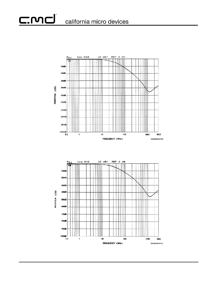
Performance Information
Typical Filter Performance (nominal conditions unless specified otherwise)
Figure 1. Microphone 1 Circuit (B1-C1) EMI Filter Performance
Figure 2. Microphone 2 Circuit (A2-C2) EMI Filter Performance
©
2005 California Micro Devices Corp. All rights reserved.
09/15/05
490 N. McCarthy Blvd., Milpitas, CA 95035-5112
Tel: 408.263.3214
Fax: 408.263.7846
www.calmicro.com
5
CM1410
Performance Information (Cont'd)
Typical Filter Performance (nominal conditions unless specified otherwise)
Figure 3. Speaker 1 Circuit (A3-C3) EMI Filter Performance
Figure 4. Speaker 2 Circuit (A4-C4) EMI Filter Performance
Document Outline