 | –≠–ª–µ–∫—Ç—Ä–æ–Ω–Ω—ã–π –∫–æ–º–ø–æ–Ω–µ–Ω—Ç: VFC110 | –°–∫–∞—á–∞—Ç—å:  PDF PDF  ZIP ZIP |

VFC110
PDS-861B
Æ
High-Frequency
VOLTAGE-TO-FREQUENCY CONVERTER
APPLICATIONS
q
INTEGRATING A/D CONVERSION
q
PROCESS CONTROL
q
VOLTAGE ISOLATION
q
VOLTAGE-CONTROLLED OSCILLATOR
q
FM TELEMETRY
FEATURES
q
HIGH-FREQUENCY OPERATION:
4MHz FS max
q
EXCELLENT LINEARITY:
±
0.02% typ at 2MHz
q
PRECISION 5V REFERENCE
q
DISABLE PIN
q
LOW JITTER
DESCRIPTION
The VFC110 voltage-to-frequency converter is a third-
generation VFC offering improved features and per-
formance. These include higher frequency operation,
an on-board precision 5V reference and a Disable
function.
The precision 5V reference can be used for offsetting
the VFC transfer function, as well as exciting trans-
ducers or bridges. The Enable pin allows several
VFCs' outputs to be paralleled, multiplexed, or simply
to shut off the VFC. The open-collector frequency
output is TTL/CMOS-compatible. The output may be
isolated by using an opto-coupler or transformer.
Internal input resistor, one-shot and integrator capaci-
tors simplify applications circuits. These components
are trimmed for a full-scale output frequency of 4MHz
at 10V input. No additional components are required
for many applications.
The VFC110 is packaged in plastic and ceramic
14-pin DIPs. Industrial and military temperature range
gradeouts are available.
International Airport Industrial Park ∑ Mailing Address: PO Box 11400, Tucson, AZ 85734 ∑ Street Address: 6730 S. Tucson Blvd., Tucson, AZ 85706 ∑ Tel: (520) 746-1111 ∑ Twx: 910-952-1111
Internet: http://www.burr-brown.com/ ∑ FAXLine: (800) 548-6133 (US/Canada Only) ∑ Cable: BBRCORP ∑ Telex: 066-6491 ∑ FAX: (520) 889-1510 ∑ Immediate Product Info: (800) 548-6132
2
14
Input Common
IN
V
1
12
I
IN
V
OUT
11
Comparator
One-Shot
V
REF
≠V
S
Analog Ground
4
13
5V
3
C
OS
6
8
Digital Ground
OUT
f
10
+V
S
7
Enable
5
© 1988 Burr-Brown Corporation
PDS-861B
Printed in U.S.A. October, 1993
2
Æ
VFC110
The information provided herein is believed to be reliable; however, BURR-BROWN assumes no responsibility for inaccuracies or omissions. BURR-BROWN assumes
no responsibility for the use of this information, and all use of such information shall be entirely at the user's own risk. Prices and specifications are subject to change
without notice. No patent rights or licenses to any of the circuits described herein are implied or granted to any third party. BURR-BROWN does not authorize or warrant
any BURR-BROWN product for use in life support devices and/or systems.
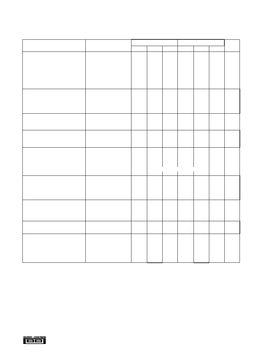
SPECIFICATIONS
At T
A
= +25
∞
C and V
S
=
±
15V, unless otherwise noted.
VFC110BG
VFC110AG/SG/AP
PARAMETER
CONDITIONS
MIN
TYP
MAX
MIN
TYP
MAX
UNITS
VOLTAGE-TO-FREQUENCY OPERATION
Nonlinearity
(1)
: f
FS
= 100kHz
C
OS
= 2.2nF, R
IN
= 44k
0.005
0.01
0.01
0.05
%FS
f
FS
= 1MHz
C
OS
= 150pF, R
IN
= 40k
0.01
0.05
0.1
%FS
f
FS
= 2MHz
C
OS
= 56pF, R
IN
= 34k
0.02
*
%FS
f
FS
= 4MHz
C
OS
= (Int), R
IN
= (Int)
1
*
%FS
Gain Error, f = 1MHz
C
OS
= 150pF, R
IN
= 40k
5
*
%
Gain Drift, f = 1MHz
Specified Temp Range
50
100
ppm/
∞
C
Relative to V
REF
Specified Temp Range
50
100
ppm/
∞
C
PSRR
V
S
=
±
8V to
±
18V
0.05
0.1
%/V
INPUT
Full Scale Input Current
250
500
*
*
µ
A
I
B
≠ (Inverting Input)
15
60
20
100
nA
I
B
+ (Non-Inverting Input)
250
*
nA
V
OS
3
3
mV
V
OS
Drift
Specified Temp Range
35
*
µ
V/
∞
C
INTEGRATOR AMPLIFIER OUTPUT
Output Voltage Range
R
L
= 2k
≠0.2
+V
S
≠ 4
*
*
V
Output Current Drive
5
20
*
*
mA
Capacitive Load
No Oscillations
10
10
nF
COMPARATOR INPUT
I
B
(Input Bias Current)
≠5
*
µ
A
Trigger Voltage
±
50
*
mV
Input Voltage Range
≠5
+V
S
*
*
V
OPEN COLLECTOR OUTPUT
V
O
Low
0.4
*
V
I
LEAKAGE
0.1
1
*
*
µ
A
Fall Time
25
*
ns
Delay to Rise
25
*
ns
Settling Time
To Specified Linearity for a
One Pulse of New Frequency Plus 1
µ
s
Full-Scale Input Step
REFERENCE VOLTAGE
Voltage
4.97
5
5.03
*
*
*
V
Voltage Drift
20
50
ppm/
∞
C
Load Regulation
I
O
= 0 to 10mA
2
10
*
*
mV
PSRR
V
S
=
±
8V to
±
18V
5
*
mV/V
Current Limit
Short Circuit
15
20
*
mA
ENABLE INPUT
V
HIGH
(f
OUT
Enabled)
Specified Temp Range
2
*
V
V
LOW
(f
OUT
Disabled)
Specified Temp Range
0.4
*
V
I
HIGH
0.1
*
µ
A
I
LOW
1
*
µ
A
POWER SUPPLY
Voltage,
±
V
S
±
8
±
15
±
18
*
*
*
V
Current
13
16
*
*
mA
TEMPERATURE RANGE
Specified
AG, BG, AP
≠25
+85
*
*
∞
C
SG
≠55
+125
∞
C
Storage
AG, BG, SG
≠65
+150
*
*
∞
C
AP
≠40
+125
*
*
∞
C
* Same specifications as VFC110BG.
NOTE: (1) Nonlinearity measured from 1V to 10V input.

3
Æ
VFC110
TEMPERATURE
PRODUCT
PACKAGE
RANGE
VFC110AG
Ceramic DIP
≠25
∞
C to +85
∞
C
VFC110BG
Ceramic DIP
≠25
∞
C to +85
∞
C
VFC110SG
Ceramic DIP
≠55
∞
C to +125
∞
C
VFC110AP
Plastic DIP
≠25
∞
C to +85
∞
C
Input Common
Analog Common
V
Comparator In
+V
NC
f
Out
Enable
Digital Ground
1
2
3
4
5
6
7
14
13
12
11
10
9
8
S
IN
IN
I
V
REF
+5V
S
≠V
OS
C
OUT
OUT
PIN CONFIGURATION
ABSOLUTE MAXIMUM RATINGS
Top View
DIP
Power Supply Voltages (+V
S
to ≠V
S
) ................................................ 40V
f
OUT
Sink Current ............................................................................ 50mA
Comparator In Voltage .......................................................... ≠5V to +V
S
Enable Input ........................................................................... +V
S
to ≠V
S
Integrator Common-Mode Voltage .................................. ≠1.5V to +1.5V
Integrator Differential Input Voltage ................................ +0.5V to ≠0.5V
Integrator Out (short-circuit) ..................................................... Indefinite
V
REF
Out (short-circuit) .............................................................. Indefinite
Operating Temperature Range
G Package ................................................................ ≠55
∞
C to +125
∞
C
P Package ................................................................... ≠40
∞
C to +85
∞
C
Storage Temperature
G Package ................................................................ ≠60
∞
C to +150
∞
C
P Package ................................................................. ≠40
∞
C to +125
∞
C
Lead Temperature (soldering, 10s) ............................................. +300
∞
C
PACKAGE INFORMATION
PACKAGE DRAWING
PRODUCT
PACKAGE
NUMBER
(1)
VFC110AG
14-Pin Ceramic DIP
169
VFC110BG
14-Pin Ceramic DIP
169
VFC110SG
14-Pin Ceramic DIP
169
VFC110AP
14-Pin Plastic DIP
010
NOTE: (1) For detailed drawing and dimension table, please see end of data
sheet, or Appendix D of Burr-Brown IC Data Book.
ORDERING INFORMATION

4
Æ
VFC110
FREQUENCY COUNT REPEATABILITY
vs COUNTER GATE TIME
1ms
Time
0.001
Frequency Repeatability (%)
0.0001
0.0002
0.0004
0.0006
0.0008
10ms
100ms
1s
17
Repeatability (Bits)
18
19
f
FS
= 1MHz
f
FS
= 100kHz
JITTER vs FULL SCALE FREQUENCY
10k
Full Scale Frequency (Hz)
500
400
300
200
100
0
Jitter (ppm)
100k
1M
10M
TYPICAL FULL SCALE GAIN DRIFT
vs FULL SCALE FREQUENCY
10k
Full Scale Frequency (Hz)
1000
100
10
Full Scale Frequency (ppm/∞C)
100k
1M
10M
A Grade,
S Grade
B Grade
REFERENCE VOLTAGE
vs REFERENCE LOAD CURRENT
0
Output Current (mA)
5.01
5
4.99
4.98
4.97
4.96
V
REF
(V)
2
4
6
8
10
12
14
16
18
20
22
Short Circuit
Current Limit
QUIESCENT CURRENT vs TEMPERATURE
≠50
Temperature (∞C)
18
16
14
12
10
8
6
4
2
0
Quiescent Current (mA)
I
Q
+
≠25
0
25
50
75
100
125
I
Q
≠
FULL-SCALE FREQUENCY
vs EXTERNAL ONE-SHOT CAPACITOR
10pF
External One-Shot Capacitor
100pF
1nF
10nF
100nF
10M
1M
100k
10k
Full Scale Frequency (Hz)
R
IN
= 40k
TYPICAL PERFORMANCE CURVES
At T
A
= +25
∞
C, V
S
=
±
15V, unless otherwise noted.
This graph describes the low frequency stability of the VFC110:
the ratio of the 1
point of the distribution of 100 runs (where
each mean frequency came from 1000 readings for each gate
time) to the overall mean frequency.
Jitter is the ratio of the 1
value of the distribution of the period
(1/f
OUT
, max) to the mean of the period.

5
Æ
VFC110
NONLINEARITY vs FULL SCALE FREQUENCY
10
Full Scale Frequency (Hz)
1
0.1
0.01
0.001
Typical Nonlinearity (% of FSR)
4
10
5
10
6
10
7
NONLINEARITY vs INPUT VOLTAGE
0
Input Voltage (V)
0.02
0.01
0
≠0.01
≠0.02
1MHz FS Linearity Error (% of FSR)
1
2
3
4
5
6
7
8
9
10
1
0.8
0.6
0.4
0.2
0
≠0.2
≠0.4
≠0.6
≠0.8
≠1
4MHz FS Linearity Error (% of FSR)
f
FS
= 4MHz
f
FS
= 1MHz
OPERATION
Figure 1 shows the connections required for operation at a
full-scale output frequency of 4MHz. Only power supply
bypass capacitors and an output pull-up resistor, R
PU
, are
required for this mode of operation. A 0V to 10V input
voltage produces a 0Hz to 4MHz output frequency. The
internal input resistor, one-shot and integrator capacitors set
the full-scale output frequency. The input is applied to the
summing junction of the integrator amplifier through the
25k
internal input resistor. Pin 14 (the non-inverting ampli-
fier input) should be referred directly to the negative side of
V
IN
. The common-mode range of the integrating amplifier is
limited to approximately ≠1V to +1V referred to analog
ground. This allows the non-inverting input to Kelvin-sense
the common connection of V
IN
, easily accommodating any
FIGURE 1. 4MHz Full-Scale Operation.
TYPICAL PERFORMANCE CURVES
(CONT)
At T
A
= +25
∞
C, V
S
=
±
15V, unless otherwise noted.
ground-drop errors. The input impedance loading V
IN
is
equal to the input resistor--approximately 25k
.
OPERATION AT LOWER FREQUENCIES
The VFC110 can be operated at lower frequencies simply by
limiting the input voltage to less than the nominal 10V full-
scale input. To maintain a 10V FS input and highest accu-
racy, however, external components are required (see Table
I). Small adjustments may be required in the nominal values
indicated. Integrator and one-shot capacitors are added in
parallel to internal capacitors. Figure 2 shows the connec-
tions required for 100kHz full scale output. The one-shot
capacitor, C
OS
, should be connected to logic ground. The
one-shot connection (pin 6) is not short-circuit protected.
Short-circuits to ground may damage the device.
2
14
IN
V
1
12
11
One-Shot
V
REF
≠V
S
Analog Ground
4
13
NC
3
6
8
Logic Ground
OUT
f
10
+V
S
7
NC
5
NC
50pF*
NC
PU
R
680
≠15V
+15V
V
L
+5V
0 to 4MHz
25k
*
0 to
+10V
* Nominal Values (±20%)