 | –≠–ª–µ–∫—Ç—Ä–æ–Ω–Ω—ã–π –∫–æ–º–ø–æ–Ω–µ–Ω—Ç: PCM1606 | –°–∫–∞—á–∞—Ç—å:  PDF PDF  ZIP ZIP |
Document Outline
- FEATURES
- APPLICATIONS
- DESCRIPTION
- functional block diagram
- Terminal Functions
- absolute maximum ratings over operating free-air temperature (unless ot\
herwise noted)
- electrical characteristics, all specifications at T A = 25C, V CC = 5 V,\
f S = 44.1 kHz,
system clock = 384 f S and 24-bit d
- timing requirements
- system clock input
- power-on reset functions
- audio serial interface
- audio data formats and timing
- functional description
- data format selection
- de-emphasis control
- analog outputs
- VCOM output
- zero flag
- zero detect condition
- zero output flag
- TYPICAL CHARACTERISTICSÑDIGITAL FILTER
- TYPICAL CHARACTERISTICSÑANALOG DYNAMIC PERFORMANCE
- APPLICATION INFORMATION
- connection diagrams
- power supply and grounding
- D/A output filter circuits
- PCB layout guidelines
- key performance parameters measurement
- total harmonic distortion + noise
- dynamic range
- idle channel signal-to-noise ratio
- MECHANICAL DATA
- DB (R-PDSO-G**) PLASTIC SMALL-OUTLINE
- IMPORTANT NOTICE
PCM1606
SLES014B ≠ OCTOBER 2001 ≠ REVISED AUGUST 2002
24-BIT, 192-kHz SAMPLING, 6-CHANNEL, ENHANCED MULTILEVEL,
DELTA-SIGMA DIGITAL-TO-ANALOG CONVERTER
1
www.ti.com
FEATURES
D
24-Bit Resolution
D
Analog Performance:
≠ Dynamic Range: 103 dB, Typical
≠ SNR: 103 dB, Typical
≠ THD+N: 0.004%, Typical
≠ Full-Scale Output: 3.1 Vp-p, Typical
D
8
◊
Oversampling Interpolation Filter:
≠ Stopband Attenuation: ≠55 dB
≠ Passband Ripple:
±
0.03 dB
D
Sampling Frequency:
≠ 5 kHz to 200 kHz (Channels 1 and 2)
≠ 5 kHz to 100 kHz (Channels 3, 4, 5, and 6)
D
Accepts 16- and 24-Bit Audio Data
D
Data Formats: Standard, I
2
S, and
Left-Justified, TDM
D
System Clock: 128 f
S
, 192 f
S
, 256 f
S
, 384 f
S
,
512 f
S
, or 768 f
S
D
Digital De-Emphasis for 32 kHz, 44.1 kHz,
48 kHz
D
Power Supply: 5-V Single Supply
D
20 -Lead SSOP Package
APPLICATIONS
D
Integrated A/V Receivers
D
DVD Movie and Audio Players
D
HDTV Receivers
D
Car Audio Systems
D
DVD Add-On Cards for High-End PCs
D
Digital Audio Workstations
D
Other Multichannel Audio Systems
DESCRIPTION
The PCM1606 is a CMOS monolithic integrated circuit
that features six 24-bit audio digital-to-analog
converters and support circuitry in a small 20-lead
SSOP package. The digital-to-analog converters utilize
Texas Instruments' enhanced multilevel, delta-sigma
architecture, which employs 2
nd
-order noise shaping
and 8-level amplitude quantization to achieve excellent
signal-to-noise performance and a high tolerance to
clock jitter.
The PCM1606 accepts industry-standard audio data
formats with 16- to 24-bit audio data. Sampling rates up
to 200 kHz are supported.
1
2
3
4
5
6
7
8
9
10
20
19
18
17
16
15
14
13
12
11
DATA1
DATA2
DATA3
FMT1
FMT0
ZEROA
AGND
V
OUT
5
V
OUT
6
V
OUT
1
SCKI
BCK
LRCK
DEMP1
DEMP0
V
CC
V
COM
V
OUT
4
V
OUT
3
V
OUT
2
PCM1606
(TOP VIEW)
PRODUCTION DATA information is current as of publication date.
Products conform to specifications per the terms of Texas Instruments
standard warranty. Production processing does not necessarily include
testing of all parameters.
Copyright
2002, Texas Instruments Incorporated
Please be aware that an important notice concerning availability, standard warranty, and use in critical applications of
Texas Instruments semiconductor products and disclaimers thereto appears at the end of this data sheet.

PCM1606
SLES014B ≠ OCTOBER 2001 ≠ REVISED AUGUST 2002
2
www.ti.com
PACKAGE/ORDERING INFORMATION
PRODUCT
PACKAGE
PACKAGE
DRAWING
NUMBER
OPERATION
TEMPERATURE
RANGE
PACKAGE
MARKING
ORDERING
NUMBER
TRANSPORT MEDIA
PCM1606E
20 Lead SSOP
ZZ334 1
25
∞
C to 85
∞
C
PCM1606E
PCM1606E
TUBE
PCM1606E
20-Lead SSOP
ZZ334-1
≠25
∞
C to 85
∞
C
PCM1606E
PCM1606E/2K
Tape and Reel
Models with a slash (/) are available only in tape and reel in the quantities indicated (e.g., /2K indicates 2000 devices per reel). Ordering 2000
pieces of PCM1606Y/2K gets a single 2000-piece tape and reel.
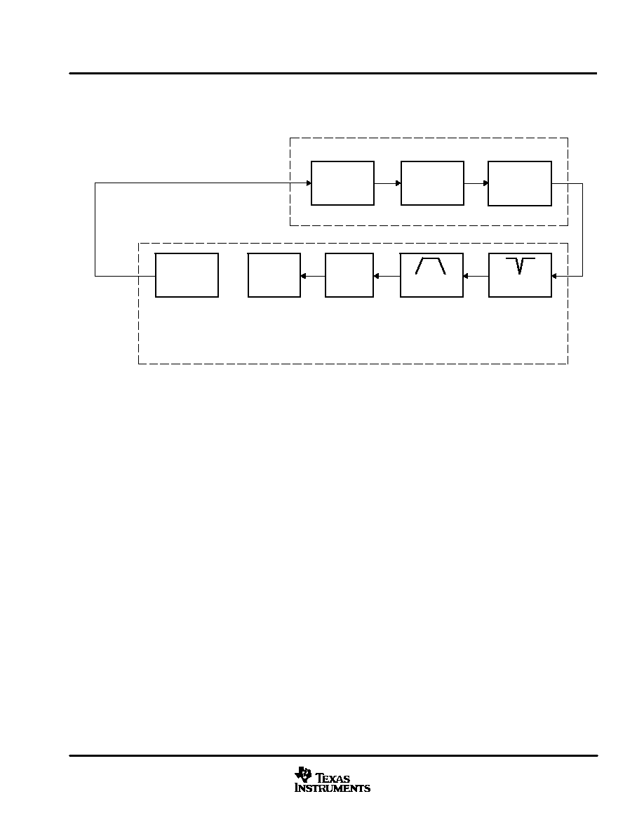
functional block diagram
Output Amp and
Low-Pass Filter
System Clock
Manager
4x / 8x
Oversampling
Digital Filter
with
Function
Controller
Enhanced
Multilevel
Delta-Sigma
Modulator
DAC
Serial
Input
I/F
Function
Control
I/F
System Clock
BCK
LRCK
DATA1(1, 2)
Zero Detect
Power Supply
DATA2(3, 4)
DATA3(5, 6)
DEMP1
DEMP0
FMT1
SCKI
FMT0
DAC
Output Amp and
DAC
DAC
Output Amp and
DAC
Output Amp and
DAC
Output Amp and
VOUT1
ZEROA
VCC
AGND
VOUT2
VOUT3
VCOM
VOUT4
VOUT5
VOUT6
Low-Pass Filter
Low-Pass Filter
Low-Pass Filter
Low-Pass Filter
Low-Pass Filter
Output Amp and
PCM1606
SLES014B ≠ OCTOBER 2001 ≠ REVISED AUGUST 2002
3
www.ti.com
Terminal Functions
TERMINAL
I/O
DESCRIPTIONS
NAME
PIN
I/O
DESCRIPTIONS
AGND
7
--
Analog and digital ground
BCK
19
I
Shift clock input for serial audio data (see Note 2)
DATA1
1
I
Serial audio data input for VOUT1 and VOUT2 (see Note 2)
DATA2
2
I
Serial audio data input for VOUT3 and VOUT4 (see Note 2)
DATA3
3
I
Serial audio data input for VOUT5 and VOUT6 (see Note 2)
DEMP0
16
I
De-emphasis control (see Note 1)
DEMP1
17
I
De-emphasis control (see Note 1)
FMT1
4
I
Format select (see Note 1)
FMT0
5
I
Format select (see Note 1)
LRCK
18
I
Left and right clock input. This clock is equal to the sampling rate, fS (see Note 2)
SCKI
20
I
System clock in. Input frequency is 128 fS, 192 fS, 256 fS, 384 fS, 512 fS or 768 fS (see Note 2)
VCC
15
--
Analog and digital power supply, 5 V
VCOM
14
--
Common voltage output. This pin should be bypassed with a 10-
µ
F capacitor to AGND
VOUT1
10
O
Voltage output for audio signal corresponding to L-channel on DATA1. Up to 192 kHz
VOUT2
11
O
Voltage output for audio signal corresponding to R-channel on DATA1. Up to 192 kHz
VOUT3
12
O
Voltage output for audio signal corresponding to L-channel on DATA2. Up to 96 kHz
VOUT4
13
O
Voltage output for audio signal corresponding to R-channel on DATA2. Up to 96 kHz
VOUT5
8
O
Voltage output for audio signal corresponding to L-channel on DATA3. Up to 96 kHz
VOUT6
9
O
Voltage output for audio signal corresponding to R-channel on DATA3. Up to 96 kHz
ZEROA
6
O
Zero-data flag. Logical AND of ZERO1 through ZERO6
NOTES:
1. Schmitt-trigger input with internal pulldown.
2. Schmitt-trigger input.
absolute maximum ratings over operating free-air temperature (unless otherwise noted)
Supply voltage, V
CC
6.5 V
. . . . . . . . . . . . . . . . . . . . . . . . . . . . . . . . . . . . . . . . . . . . . . . . . . . . . . . . . . . . . . . . . . . . . . . . . . .
Digital input voltage
≠
0.3 V to V
CC
+ 0.3 V
. . . . . . . . . . . . . . . . . . . . . . . . . . . . . . . . . . . . . . . . . . . . . . . . . . . . . . . . . . . . . .
Analog input voltage
≠
0.3 V to V
CC
+ 0.3 V
. . . . . . . . . . . . . . . . . . . . . . . . . . . . . . . . . . . . . . . . . . . . . . . . . . . . . . . . . . . . .
Input current (except power supply)
±
10 mA
. . . . . . . . . . . . . . . . . . . . . . . . . . . . . . . . . . . . . . . . . . . . . . . . . . . . . . . . . . . .
Ambient temperature under bias
≠
40
∞
C to 125
∞
C
. . . . . . . . . . . . . . . . . . . . . . . . . . . . . . . . . . . . . . . . . . . . . . . . . . . . . . . .
Storage temperature
≠
55
∞
C to 150
∞
C
. . . . . . . . . . . . . . . . . . . . . . . . . . . . . . . . . . . . . . . . . . . . . . . . . . . . . . . . . . . . . . . . . .
Junction temperature
150
∞
C
. . . . . . . . . . . . . . . . . . . . . . . . . . . . . . . . . . . . . . . . . . . . . . . . . . . . . . . . . . . . . . . . . . . . . . . . . .
Lead temperature (soldering, 5s)
260
∞
C, 5s
. . . . . . . . . . . . . . . . . . . . . . . . . . . . . . . . . . . . . . . . . . . . . . . . . . . . . . . . . . . . .
Package temperature (IR reflow, 10s)
235
∞
C, 10s
. . . . . . . . . . . . . . . . . . . . . . . . . . . . . . . . . . . . . . . . . . . . . . . . . . . . . . . .
Stresses beyond those listed under "absolute maximum ratings" may cause permanent damage to the device. These are stress ratings only, and
functional operation of the device at these or any other conditions beyond those indicated under "recommended operating conditions" is not
implied. Exposure to absolute-maximum-rated conditions for extended periods may affect device reliability.

PCM1606
SLES014B ≠ OCTOBER 2001 ≠ REVISED AUGUST 2002
4
www.ti.com
electrical characteristics, all specifications at T
A
= 25
∞
C, V
CC
= 5 V, f
S
= 44.1 kHz,
system clock = 384 f
S
and 24-bit data (unless otherwise noted)
PARAMETER
TEST CONDITIONS
PCM1606E
UNIT
PARAMETER
TEST CONDITIONS
MIN
TYP
MAX
UNIT
RESOLUTION
24
Bits
DATA FORMAT
Audio data interface format
Standard, I2S, Left-Justified, TDM
Audio data bit length
16 or 24 bits, selectable
Audio data format
MSB first, 2s complement
f
Sampling frequency
VOUT1, VOUT2
5
200
kHz
fS
Sampling frequency
VOUT3, VOUT4, VOUT5, VOUT6
5
100
kHz
System clock frequency
128, 192, 256, 384, 512, 768 fS
DIGITAL INPUT/OUTPUT
Logic family (TTL compatible)
VIH
High-level input voltage
2
V
VIL
Low-level input voltage
0.8
V
IIH
High-level input current
VIN = VCC
67
100
µ
A
IIL
Low-level input current
VIN = 0 V
≠10
µ
A
VOH
High-level output voltage
IOH = ≠4 mA
2.4
V
VOL
Low-level output voltage
IOL = 4 mA
1
V
DYNAMIC PERFORMANCE
fS = 44.1 kHz/384 fS
0.004%
0.01%
VOUT = 0 dB
fS = 96 kHz/256 fS
0.005%
THD+N
Total harmonic
VOUT 0 dB
fS = 192 kHz/128 fS
0.002%
THD+N
Total harmonic
distortion plus noise
fS = 44.1 kHz/348 fS
1%
VOUT = ≠60 dB fS = 96 kHz / 256 fS
1.2%
VOUT 60 dB
fS = 192 kHz/128 fS
1%
EIAJ, A-weighted, fS = 44.1 kHz/384 fS
98
103
Dynamic range
A-weighted, fS = 96 kHz/256 fS
99
dB
Dynamic range
A-weighted, fS = 192 kHz/128 fS
101
dB
EIAJ, A-weighted, fS = 44.1 kHz/384 fS
98
103
Signal-to-noise ratio
A-weighted, fS = 96 kHz/256 fS
100
dB
Signal to noise ratio
A-weighted, fS = 192 kHz/128 fS
101
dB
fS = 44.1 kHz/384 fS
95
100
Channel separation
fS = 96 kHz/256 fS
95
dB
Channel se aration
fS = 192 kHz/128 fS
100
dB
Level linearity error
VOUT = ≠90 dB
±
0.5
dB
DC ACCURACY
Gain error
±
1 %FSR
Gain mismatch, channel-to-channel
±
1.3 %FSR
Bipolar zero error
VOUT = 0.5 VCC at BPZ
±
30
mV
ANALOG OUTPUT
Output voltage
Full scale (≠0 dB)
62% of VCC
Vp-p
Center voltage
50% of VCC
Vdc
Load impedance
Ac load
5
k
PCM1606
SLES014B ≠ OCTOBER 2001 ≠ REVISED AUGUST 2002
5
www.ti.com
electrical characteristics, all specifications at T
A
= 25
∞
C, V
CC
= 5 V, f
S
= 44.1 kHz,
system clock = 384 f
S
and 24-bit data (unless otherwise noted) (continued)
PARAMETER
TEST CONDITIONS
PCM1606E
UNIT
PARAMETER
TEST CONDITIONS
MIN
TYP
MAX
UNIT
DIGITAL FILTER PERFORMANCE
FILTER CHARACTERISTICS
Passband
±
0.03 dB
0.454 fS
Passband
≠3 dB
0.487 fS
Stopband
0.546 fS
Passband ripple
±
0.03
dB
Stopband attenuation
Stopband = 0.546 fS
≠50
dB
Stopband attenuation
Stopband = 0.567 fS
≠55
dB
ANALOG FILTER PERFORMANCE
Frequency response
At 20 kHz
≠0.03
dB
POWER SUPPLY REQUIREMENTS (see Note 4)
VCC
Voltage range
4.5
5
5.5
VDC
fS = 44.1 kHz/384 fS
50
65
ICC
Supply current
fS = 96 kHz/256 fS
72
mA
ICC
Su
ly current
fS = 192 kHz/128 fS
68
mA
fS = 44.1 kHz/384 fS
250
358
Power dissipation
fS = 96 kHz/256 fS
360
mW
Power dissi ation
fS = 192 kHz/128 fS
340
mW
TEMPERATURE RANGE
Operation temperature
≠25
85
∞
C
JA
Thermal resistance
20-pin SSOP
115
∞
C/W
NOTES:
3. Analog performance specs are tested using System Two Cascade Plus by Audio Precision with 400-Hz HPF, 30-kHz LPF on at RMS
with 20-kHz LPF, 400-Hz HPF in calculation.
Shibasoku #725 THD meter, 400 Hz HPF, 30 kHz LPF on, at average mode with 20-kHz bandwidth limiting. The load connected
to the analog output is 5 k
or larger via capacitance coupling.
4. Condition in 192-kHz operation is channel 3 through channel 6 are disabled.
timing requirements
system clock input
The PCM1606 requires a system clock for operating the digital interpolation filters and multilevel delta-sigma
modulators. The system clock is applied at the SCKI (pin 20). Table 1 shows examples of system clock
frequencies for common audio sampling rates.
Figure 1 shows the timing requirements for the system clock input. For optimal performance, it is important to
use a clock source with low phase jitter and noise. Texas Instruments' PLL1700 multiclock generator is an
excellent choice for providing the PCM1606 system clock source.
The 192-kHz sampling frequency operation is available on DATA1 for V
OUT
1 and V
OUT
2. When the system clock
of 128 f
S
or 192 f
S
is detected, V
OUT
3, V
OUT
4, V
OUT
5 and V
OUT
6 are automatically forced to the bipolar zero
level (= 0.5 V
CC
). Table 1 lists the typical system clock frequency.

PCM1606
SLES014B ≠ OCTOBER 2001 ≠ REVISED AUGUST 2002
6
www.ti.com
timing requirements (continued)
power-on reset functions
The PCM1606 includes a power-on reset function. Figure 2 shows the operation of this function. With the
system clock active and V
CC
> 3 V typical (2.2 V to 3.7 V), the power-on reset function is enabled. The
initialization sequence requires 1024 system clocks from the time V
CC
> 3 V. After the initialization period, the
PCM1606 is set to its reset default state.
Table 1. System Clock Rates for Common Audio Sampling Frequencies
SAMPLING FREQUENCY
SYSTEM CLOCK FREQUENCY (fSCLK) (MHz)
SAMPLING FREQUENCY
128 fS
192 fS
256 fS
384 fS
512 fS
768 fS
8 kHz
--
--
2.048
3.072
4.096
6.144
16 kHz
--
--
4.096
6.144
8.192
12.288
32 kHz
--
--
8.192
12.288
16.384
24.576
44.1 kHz
--
--
11.2896
16.9344
22.5792
33.8688
48 kHz
--
--
12.288
18.432
24.576
36.864
96 kHz
--
--
24.576
36.864
49.152
See Note 5
192 kHz
24.576
36.864
See Note 6
See Note 6
See Note 6
See Note 6
NOTES:
5. The 768-fS system clock rate is not supported for fS > 64 kHz.
6. This system clock is not supported for the given sampling frequency.
t(SCKH)
System Clock
Pulse Cycle Time
System Clock
t(SCKL)
2.0 V
0.8 V
1/128 fS, 1/256 fS, 1/384 fS, 1/512 fS and 1/768 fS.
PARAMETERS
MIN
MAX
UNIT
t(SCKH)
System clock pulse duration HIGH
10
ns
t(SCKL)
System clock pulse duration LOW
10
ns
Figure 1. System Clock Timing
1024 System Clocks
System Clock
Internal Reset
3.7 V
3.0 V
2.2 V
VDD
0 V
Don't Care
Reset
Reset Removal
Figure 2. Power-On Reset Timing

PCM1606
SLES014B ≠ OCTOBER 2001 ≠ REVISED AUGUST 2002
7
www.ti.com
timing requirements (continued)
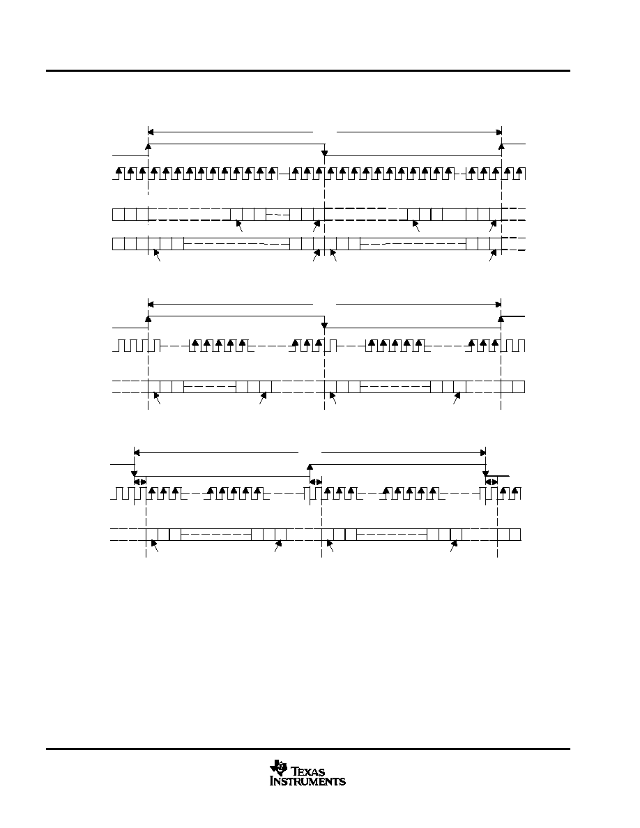
audio serial interface
The audio serial interface for the PCM1606 comprises a 5-wire synchronous serial port. It includes LRCK (pin
18), BCK (pin 19), DATA1 (pin 1), DATA2 (pin 2) and DATA3 (pin 3). BCK is the serial audio bit clock and is used
to clock the serial data present on DATA1, DATA2, and DATA3 into the audio interface serial shift registers. Serial
data is clocked into the PCM1606 on the rising edge of BCK. LRCK is the serial audio left/right word clock. LRCK
is used to latch serial data into the serial audio interface internal registers.
Both LRCK and BCK must be synchronous to the system clock. Ideally, it is recommended that LRCK and BCK
be derived from the system clock input or output, SCKI. The left/right clock, LRCK, is operated at the sampling
frequency (f
S
). The bit clock, BCK, may be operated at 32, 48, or 64 times the sampling frequency.
audio data formats and timing
The PCM1606 supports industry-standard audio data formats, including standard, I
2
S, left-justified, and TDM.
The data formats are shown in Figure 6. Data formats are selected using the format pins, FMT1 (pin 4) and
FMT0 (pin 5). All formats require binary 2s complement, MSB-first audio data. Figure 3 shows a detailed timing
diagram for the serial audio interface, with the exception of TDM format.
DATA1, DATA2, and DATA3 each carry two audio channels, designated as the left and right channels. The left
channel data always precedes the right channel data in the serial data stream for all data formats. Table 2 shows
the mapping of the digital input data to the analog output pins.
TDM format is able to interface by 3-wire synchronous serial port. All data inputs from DATA1, BCK can be
operated at 128, 256, and 512 times the sampling frequency. The rising edge of LRCK means the start of a data
frame. Only channel 1 and channel 2 data are acceptable at the 192-kHz sampling frequency (f
S
); channel 3,
channel 4, channel 5, and channel 6 data are don't care.
Figure 4 shows the timing requirements for BCK input for TDM format. Figure 5 shows the detailed timing
diagram for TDM format.
Table 2. Audio Input Data to Analog Output Mapping
DATA INPUT
CHANNEL
ANALOG OUTPUT
DATA1
Left
VOUT1
DATA1
Right
VOUT2
DATA2
Left
VOUT3
DATA2
Right
VOUT4
DATA3
Left
VOUT5
DATA3
Right
VOUT6
Up to 192 kHz
Up to 96 kHz

PCM1606
SLES014B ≠ OCTOBER 2001 ≠ REVISED AUGUST 2002
8
www.ti.com
timing requirements (continued)
DATA1, DATA2, DATA3
t(BCH)
1.4 V
1.4 V
1.4 V
BCK
LRCK
t(BCL)
t(LB)
t(BCY)
t(BL)
tsu(D)
th(D)
PARAMETER
MIN
MAX
UNIT
t(BCY)
BCK pulse cycle time
32 fS / 48 fS / 64
fS
t(BCH)
BCK high-level time
35
ns
t(BCL)
BCK low-level time
35
ns
t(BL)
BCK rising edge to LRCK edge
10
ns
t(LB)
LRCK falling edge to BCK rising edge
10
ns
tsu(D)
DATA setup time
10
ns
th(D)
DATA hold time
10
ns
fS is the sampling frequency (e.g., 44.1 kHz, 48 kHz, 96 kHz, etc.)
Figure 3. Audio Interface Timing
Table 3. Bit Clock Rates for TDM Format Sampling Frequencies
SAMPLING
SYSTEM CLOCK FREQUENCY (fSCKI) (MHz)
SAMPLING
FREQUENCY
128 fS
256 fS
512 fS
8 kHz
--
2.048
4.096
16 kHz
--
4.096
8.192
32 kHz
--
8.192
16.384
44.1 kHz
--
11.2896
22.5792
48 kHz
--
12.288
24.576
96 kHz
--
24.576
49.152
192 kHz
24.576
See Note 7
See Note 7
NOTE 7: This bit clock is not supported for the given sampling frequency.

PCM1606
SLES014B ≠ OCTOBER 2001 ≠ REVISED AUGUST 2002
9
www.ti.com
timing requirements (continued)
t(BCKH)
Bit Clock Pulse
Cycle Time
BCK
t(BCKL)
2.0 V
0.8 V
PARAMETERS
MIN
MAX
UNIT
t(BCKH)
Bit clock pulse duration HIGH
10
ns
t(BCKL)
Bit clock pulse duration LOW
10
ns
1/128 fS, 1/256 fS, and 1/512 fS.
Figure 4. Bit Clock Timing for TDM Format
DATA1
t(BCH)
1.4 V
1.4 V
1.4 V
BCK
LRCK
t(BCL)
t(LB)
t(BCY)
tsu(D)
th(D)
t(BL)
PARAMETER
MIN
MAX
UNIT
t(BCY)
BCK pulse cycle time
20
ns
t(BCH)
BCK high-level time
10
ns
t(BCL)
BCK low-level time
10
ns
t(BL)
BCK rising edge to LRCK edge
7
ns
t(LB)
LRCK falling edge to BCK rising edge
7
ns
tsu(D)
DATA setup time
7
ns
th(D)
DATA hold time
7
ns
Figure 5. Audio Interface Timing for TDM Format
PCM1606
SLES014B ≠ OCTOBER 2001 ≠ REVISED AUGUST 2002
10
www.ti.com
timing requirements (continued)
LRCK
BCK
R≠Channel
L≠Channel
DATA 14 15 16
1
2
15 16
MSB
LSB
3
14
1
2
15 16
MSB
LSB
3
14
DATA 14 15 16
1
2
15 16
MSB
LSB
3
14
1
2
15 16
MSB
LSB
3
14
LRCK
BCK
R≠Channel
L≠Channel
DATA
1
2
N≠1
N
MSB
LSB
3
N≠2
1
2
N≠1
N
MSB
LSB
3
N≠2
1
2
LRCK
BCK
R≠Channel
L≠Channel
DATA
1
2
N≠1
N
MSB
LSB
3
N≠2
1
2
N≠1
N
MSB
LSB
3
N≠2
1
2
1/fS
(= 32 fS, 48 fS or 64 fS)
16-Bit Right-Justified, BCK = 48 fS or 64 fS
16-Bit Right-Justified, BCK = 32 fS
1/fS
1/fS
(= 48 fS or 64 fS)
(1) Standard Data Format; L-Channel = HIGH, R-Channel = LOW
(2) Left-Justified Data Format; L-Channel = HIGH, R-Channel = LOW
(3) I
2
S Data Format; L-Channel = LOW, R-Channel = HIGH
Figure 6. Audio Data Input Format
PCM1606
SLES014B ≠ OCTOBER 2001 ≠ REVISED AUGUST 2002
11
www.ti.com
timing requirements (continued)
LRCK
BCK
LOW Fix
1
23
MSB
1
2
24
3
22
Channel 1
24
Channel 2
Channel 6
1
2
LOW Fix 64 Bit
LRCK
BCK
1
23
1
2
24
3
22
24
1
2
LRCK
BCK
LOW Fix
1
1
2
24
LOW Fix
1
LOW Fix
64 BCK
64 BCK
Channel 1
LOW Fix
LOW Fix
LOW Fix
LOW Fix 64 Bit
Channel 1
Channel 2
Channel 3
Channel 6
LSB
LSB
MSB
MSB
LSB
MSB
LSB
1/fS
BCK = 256 fS
1/fS
BCK = 128 fS
1/fS
BCK = 512 fS
Channel 2
(4) TDM Data Format
Channel 3
32 BCK
32 BCK
32 BCK
32 BCK
Figure 6. Audio Data Input Format (Continued)
functional description
The PCM1606 has several built-in functions including digital input data format selection and digital
de-emphasis. These functions are hardware controlled with static control signals and used on pin FMT1 (pin 4),
pin FMT0 (pin 5), pin DEMP1 (pin 17), and DEMP0 (pin 16).
data format selection
The PCM audio data format can be selected by pin FMT1 (pin 4) and FMT0 (pin 5) as shown in Table 4.
Table 4. Data Format Control
FMT1 (pin 4)
FMT0 (pin 5)
AUDIO INTERFACE
LOW
LOW
I2S
LOW
HIGH
TDM
HIGH
LOW
Standard
HIGH
HIGH
Left-justified

PCM1606
SLES014B ≠ OCTOBER 2001 ≠ REVISED AUGUST 2002
12
www.ti.com
functional description (continued)
de-emphasis control
The de-emphasis control can be selected by DEMP1 (pin 17) and DEMP0 (pin 16). See Table 5.
Table 5. De-Emphasis Control
DEMT1 (pin 17)
DEMT0 (pin 16)
AUDIO INTERFACE
LOW
LOW
OFF
LOW
HIGH
48 kHz
HIGH
LOW
44.1 kHz
HIGH
HIGH
32 kHz
analog outputs
The PCM1606 includes six independent output channels, V
OUT
1 through V
OUT
6. These are unbalanced
outputs, each capable of driving 3.1 Vp-p typical into a 5-k
ac load with V
CC
= 5 V. The internal output amplifiers
for V
OUT
1 through V
OUT
6 are dc-biased to the common-mode (or bipolar zero) voltage, equal to V
CC
/2.
The output amplifiers include an RC continuous-time filter, which helps to reduce the out-of-band noise energy
present at the DAC outputs due to the noise shaping characteristics of the PCM1606's delta-sigma D/A
converters. The frequency response of this filter is shown in Figure 7. By itself, this filter is not enough to
attenuate the out-of-band noise to an acceptable level for most applications. An external low-pass filter is
required to provide sufficient out-of-band noise rejection. Further discussion of DAC post-filter circuits is
provided in the Application Information section of this data sheet.
f ≠ Frequency ≠ Hz
≠100
≠80
≠60
≠40
≠20
0
20
Level
≠
dB
LEVEL
vs
FREQUENCY
1
10
100
1k
10k
100k
1M
10M
Figure 7. Output Filter Frequency Response

PCM1606
SLES014B ≠ OCTOBER 2001 ≠ REVISED AUGUST 2002
13
www.ti.com
functional description (continued)
V
COM
output
One unbuffered common-mode voltage output pin, V
COM
(pin 14) is brought out for decoupling purposes. This
pin is nominally biased to a dc voltage level equal to V
CC
/2. If this pin is to be used to bias external circuitry, a
voltage follower is required for buffering purposes. Figure 8 shows an example of using the V
COM
pin for external
biasing applications.
14
PCM1606
V
BIAS
[
V
CC
2
4
VCOM
3
1
OPA337
≠
+
10
µ
F
+
Figure 8. Biasing External Circuits Using the V
COM
Pin
zero flag
zero detect condition
Zero detection for each output channel is independent from the others. If the data for a given channel remains
at a 0 level for 1024 sample periods (or LRCK clock periods), a zero detect condition exists for that channel.
zero output flag
When the data for all channels remains at a 0 level for 1024 sample periods (or LRCK clock periods), the ZEROA
(pin 6) is set to a logic 1 state. The zero flag pin can be used to operate external mute circuits, or used as a status
indicator for a microcontroller, audio signal processor, or other digitally controlled functions.

PCM1606
SLES014B ≠ OCTOBER 2001 ≠ REVISED AUGUST 2002
14
www.ti.com
TYPICAL CHARACTERISTICS--DIGITAL FILTER
Figure 9
f ≠ Frequency [
fS]
≠140
≠120
≠100
≠80
≠60
≠40
≠20
0
0
1
2
3
4
VCC = 5 V
fS = 44.1 kHz
TA = 25
∞
C
De-emphasis Off
Amplitude
≠
dB
AMPLITUDE
vs
FREQUENCY
Figure 10
f ≠ Frequency [
fS]
≠0.05
≠0.04
≠0.03
≠0.02
≠0.01
0.00
0.01
0.02
0.03
0.04
0.05
0.0
0.1
0.2
0.3
0.4
0.5
VCC = 5 V
fS = 44.1 kHz
TA = 25
∞
C
De-emphasis Off
Amplitude
≠
dB
AMPLITUDE
vs
FREQUENCY
Figure 11
f ≠ Frequency ≠ kHz
≠10
≠9
≠8
≠7
≠6
≠5
≠4
≠3
≠2
≠1
0
0
2
4
6
8
10
12
14
VCC = 5 V
fS = 32 kHz
TA = 25
∞
C
De-emphasis Level
≠
dB
DE-EMPHASIS LEVEL
vs
FREQUENCY
Figure 12
f ≠ Frequency ≠ kHz
≠0.5
≠0.4
≠0.3
≠0.2
≠0.1
≠0.0
0.1
0.2
0.3
0.4
0.5
0
2
4
6
8
10
12
14
VCC = 5 V
fS = 32 kHz
TA = 25
∞
C
De-emphasis Error
≠
dB
DE-EMPHASIS ERROR
vs
FREQUENCY
All specifications at TA = 25
∞
C, VCC = 5 V, fS = 44.1 kHz, system clock = 384 fS and 24-bit data, unless otherwise noted.

PCM1606
SLES014B ≠ OCTOBER 2001 ≠ REVISED AUGUST 2002
15
www.ti.com
TYPICAL CHARACTERISTICS--DIGITAL FILTER
Figure 13
f ≠ Frequency ≠ kHz
≠10
≠9
≠8
≠7
≠6
≠5
≠4
≠3
≠2
≠1
0
0
2
4
6
8
10
12
14
16
18
20
VCC = 5 V
fS = 44.1 kHz
TA = 25
∞
C
De-emphasis Level
≠
dB
DE-EMPHASIS LEVEL
vs
FREQUENCY
Figure 14
f ≠ Frequency ≠ kHz
≠0.5
≠0.4
≠0.3
≠0.2
≠0.1
≠0.0
0.1
0.2
0.3
0.4
0.5
0
2
4
6
8
10
12
14
16
18
20
VCC = 5 V
fS = 44.1 kHz
TA = 25
∞
C
De-emphasis Error
≠
dB
DE-EMPHASIS ERROR
vs
FREQUENCY
Figure 15
f ≠ Frequency ≠ kHz
≠10
≠9
≠8
≠7
≠6
≠5
≠4
≠3
≠2
≠1
0
0
2
4
6
8
10
12
14
16
18
20
22
VCC = 5 V
fS = 48 kHz
TA = 25
∞
C
De-emphasis Level
≠
dB
DE-EMPHASIS LEVEL
vs
FREQUENCY
Figure 16
f ≠ Frequency ≠ kHz
≠0.5
≠0.4
≠0.3
≠0.2
≠0.1
≠0.0
0.1
0.2
0.3
0.4
0.5
0
2
4
6
8
10
12
14
16
18
20
22
VCC = 5 V
fS = 48 kHz
TA = 25
∞
C
De-emphasis Error
≠
dB
DE-EMPHASIS ERROR
vs
FREQUENCY
All specifications at TA = 25
∞
C, VCC = 5 V, fS = 44.1 kHz, system clock = 384 fS and 24-bit data, unless otherwise noted.
PCM1606
SLES014B ≠ OCTOBER 2001 ≠ REVISED AUGUST 2002
16
www.ti.com
TYPICAL CHARACTERISTICS--ANALOG DYNAMIC PERFORMANCE
Figure 17
0.01
0.10
1.00
10.00
100.00
4.0
4.5
5.0
5.5
6.0
VCC ≠ Supply Voltage ≠ V
VCC = 5 V
fS = 44.1 kHz
TA = 25
∞
C
THD+N
≠
T
otal Harmonic Distortion + Noise
≠
%
TOTAL HARMONIC DISTORTION + NOISE
vs
SUPPLY VOLTAGE
44.1 kHz
384 fS
≠60 dB
0 dB
96 kHz
256 fS
192 kHz
128 fS
44.1 kHz
384 fS
96 kHz
256 fS
10
1
0.1
0.01
0.001
192 kHz
128 fS
Figure 18
VCC ≠ Supply Voltage ≠ V
96
98
100
102
104
106
4.0
4.5
5.0
5.5
6.0
VCC = 5 V
fS = 44.1 kHz
TA = 25
∞
C
Dynamic Range
≠
dB
DYNAMIC RANGE
vs
SUPPLY VOLTAGE
44.1 kHz
384 fS
192 kHz
128 fS
96 kHz
256 fS
Figure 19
VCC ≠ Supply Voltage ≠ V
96
98
100
102
104
106
4.0
4.5
5.0
5.5
6.0
VCC = 5 V
fS = 44.1 kHz
TA = 25
∞
C
SNR
≠
dB
SNR
vs
SUPPLY VOLTAGE
44.1 kHz
384 fS
192 kHz
128 fS
96 kHz
256 fS
Figure 20
VCC ≠ Supply Voltage ≠ V
92
94
96
98
100
102
104
4.0
4.5
5.0
5.5
6.0
VCC = 5 V
fS = 44.1 kHz
TA = 25
∞
C
Channel Separation
≠
dB
CHANNEL SEPARATION
vs
SUPPLY VOLTAGE
44.1 kHz
384 fS
192 kHz
128 fS
96 kHz
256 fS
All specifications at TA = 25
∞
C, VCC = 5 V, fS = 44.1 kHz, system clock = 384 fS and 24-bit data, unless otherwise noted.

PCM1606
SLES014B ≠ OCTOBER 2001 ≠ REVISED AUGUST 2002
17
www.ti.com
TYPICAL CHARACTERISTICS--ANALOG DYNAMIC PERFORMANCE
Figure 21
0.01
0.10
1.00
10.00
100.00
≠50
≠25
0
25
50
75
100
TA ≠ Free-Air Temperature ≠
∞
C
VCC = 5 V
fS = 44.1 kHz
THD+N
≠
T
otal Harmonic Distortion + Noise
≠
%
TOTAL HARMONIC DISTORTION + NOISE
vs
FREE-AIR TEMPERATURE
44.1 kHz
384 fS
≠60 dB
0 dB
96 kHz
256 fS
192 kHz
128 fS
192 kHz
128 fS
44.1 kHz
384 fS
96 kHz
256 fS
10
1
0.1
0.01
0.001
Figure 22
TA ≠ Free-Air Temperature ≠
∞
C
96
98
100
102
104
106
≠50
≠25
0
25
50
75
100
VCC = 5 V
fS = 44.1 kHz
Dynamic Range
≠
dB
DYNAMIC RANGE
vs
FREE-AIR TEMPERATURE
44.1 kHz
384 fS
192 kHz
128 fS
96 kHz
256 fS
Figure 23
TA ≠ Free-Air Temperature ≠
∞
C
94
96
98
100
102
104
106
≠50
≠25
0
25
50
75
100
VCC = 5 V
fS = 44.1 kHz
SNR
≠
dB
SNR
vs
FREE-AIR TEMPERATURE
44.1 kHz
384 fS
192 kHz
128 fS
96 kHz
256 fS
Figure 24
TA ≠ Free-Air Temperature ≠
∞
C
92
94
96
98
100
102
104
≠50
≠25
0
25
50
75
100
VCC = 5 V
fS = 44.1 kHz
Channel Separation
≠
dB
CHANNEL SEPARATION
vs
FREE-AIR TEMPERATURE
44.1 kHz
384 fS
192 kHz
128 fS
96 kHz
256 fS
All specifications at TA = 25
∞
C, VCC = 5 V, fS = 44.1 kHz, system clock = 384 fS and 24-bit data, unless otherwise noted.

PCM1606
SLES014B ≠ OCTOBER 2001 ≠ REVISED AUGUST 2002
18
www.ti.com
TYPICAL CHARACTERISTICS--ANALOG DYNAMIC PERFORMANCE
Figure 25
f ≠ Frequency ≠ MHz
≠180
≠160
≠140
≠120
≠100
≠80
≠60
≠40
≠20
0
0.0
0.5
1.0
1.5
2.0
VCC = 5 V
fS = 44.1 kHz
TA = 25
∞
C
Amplitude
≠
dB
≠90-dB OUTPUT SPECTRUM
Figure 26
f ≠ Frequency ≠ MHz
≠180
≠160
≠140
≠120
≠100
≠80
≠60
≠40
≠20
0
0.0
0.1
0.2
0.3
0.4
VCC = 5 V
fS = 44.1 kHz
TA = 25
∞
C
Amplitude
≠
dB
≠90-dB OUTPUT SPECTRUM
Figure 27
Jitter ≠ ps
90
92
94
96
98
100
102
104
106
0
100
200
300
400
500
600
VCC = 5 V
fS = 44.1 kHz
TA = 25
∞
C
Dynamic Range
≠
dB
DYNAMIC RANGE
vs
JITTER
All specifications at TA = 25
∞
C, VCC = 5 V, fS = 44.1 kHz, system clock = 384 fS and 24-bit data, unless otherwise noted.

PCM1606
SLES014B ≠ OCTOBER 2001 ≠ REVISED AUGUST 2002
19
www.ti.com
APPLICATION INFORMATION
connection diagrams
A basic connection diagram is shown in Figure 28, with the necessary power supply bypassing and decoupling
components. Texas Instruments recommends using the component values shown in Figure 28 for all designs.
A typical application diagram is shown in Figure 29. Texas Instruments' PLL1700 is used to generate the system
clock input at SCKI, as well as generating the clock for the audio signal processor.
The use of series resistors (22
to 100
) is recommended for SCKI, LRCK, BCK, DATA1, DATA2, and DATA3.
The series resistor combines with the stray PCB and device input capacitance to form a low-pass filter which
removes high-frequency noise from the digital signal, thus, reducing high-frequency emission.
DATA1
20
19
18
17
16
15
14
13
12
11
1
2
3
4
5
6
7
8
9
10
+
PCM1606
DATA2
DATA3
FMT1
FMT0
ZEROA
AGND
VOUT5
VOUT6
VOUT1
SCKI
VOUT4
BCK
LRCK
DEMP1
DEMP0
VOUT3
VOUT2
VCOM
VCC
10
µ
F
Microcontroller
ML
PLL1700
MC
MD
10
µ
F
+
+5 V Power Supply
BCK
LRCK
DEMP1
DEMP0
LPF
LPF
LPF
DATA1
DATA2
DATA3
FMT1
FMT0
ZEROA
LPF
LPF
LPF
SCKO3
Figure 28. Basic Connection Diagram

PCM1606
SLES014B ≠ OCTOBER 2001 ≠ REVISED AUGUST 2002
20
www.ti.com
APPLICATION INFORMATION
DATA1
20
19
18
17
16
15
14
13
12
11
1
2
3
4
5
6
7
8
9
10
PLL1700
L
R
LF
RF
RS
LS
CTR
SUB
XT1
Buffer
Master Clock
+
+
+
+
+
+
+
+
Down Mix
ANALOG SECTION
DIGITAL SECTION
PCM1606
DATA2
DATA3
FMT1
FMT0
ZEROA
AGND
VOUT5
VOUT6
VOUT1
SCKI
VOUT4
BCK
LRCK
DEMP1
DEMP0
VOUT3
VOUT2
VCOM
VCC
µ
C/
µ
P
{
Audio DSP
or
Decoder
RS
w
RS
RS
RS
RS
RS
10
µ
F
10
µ
F
10
µ
F
10
µ
F
10
µ
F
10
µ
F
10
µ
F
10
µ
F
0.1
µ
F
SCKO3
}
Output
Low-Pass
Filters
W
27-MHz
5-V Analog
Format and de-emphasis control can be provided by the DSP/decoder.
Actual clock output used is determined by the application.
ß RS = 22
to 100
∂ See the Application Information section of this data sheet for more information.
Figure 29. Typical Application Diagram
power supply and grounding
The PCM1606 requires a 5-V supply. The 5-V supply is used to power the DAC analog output-filter circuitry, the
digital filter, and the serial interface circuitry.
Two capacitors are required for supply bypassing, as shown in Figure 29. These capacitors should be located
as close as possible to the PCM1606 package. The 10-
µ
F capacitors should be tantalum or aluminum
electrolytic, while the 0.1-
µ
F capacitors are ceramic (X7R type is recommended for surface-mount
applications).
PCM1606
SLES014B ≠ OCTOBER 2001 ≠ REVISED AUGUST 2002
21
www.ti.com
APPLICATION INFORMATION
D/A output filter circuits
Delta-sigma D/A converters utilize noise shaping techniques to improve in-band signal-to-noise ratio (SNR)
performance at the expense of generating increased out-of-band noise above the Nyquist frequency, or f
S
/2.
The out-of-band noise must be low-pass filtered in order to provide optimal converter performance. This is
accomplished by a combination of on-chip and external low-pass filtering.
Figure 30 and Figure 31 show the recommended external low-pass active filter circuits for dual- and
single-supply applications. These circuits are 2nd-order Butterworth filters using the multiple feedback (MFB)
circuit arrangement, which reduces sensitivity to passive component variations over frequency and
temperature. For more information regarding MFB active filter design, see your local Texas Instruments sales
office.
Because the overall system performance is defined by the quality of the D/A converters and their associated
analog output circuitry, high-quality audio op amps are recommended for the active filters. Texas Instruments'
OPA2134 and OPA2353 dual op amps are shown in Figure 30 and Figure 31, and are recommended for use
with the PCM1606.
2
3
1
OPA2134
≠
+
VOUT
R4
C2
C1
R3
R2
R1
VIN
A
V
[ *
R
2
R
1
Figure 30. Dual-Supply Filter Circuit
2
3
1
OPA2134
≠
+
VOUT
R4
C2
C1
R3
R2
R1
VIN
A
V
[ *
R
2
R
1
OPA337
≠
+
PCM1606
VCOM
C2
10
µ
F
+
To Additional
Low-Pass Filter
Circuits
Figure 31. Single-Supply Filter Circuit

PCM1606
SLES014B ≠ OCTOBER 2001 ≠ REVISED AUGUST 2002
22
www.ti.com
APPLICATION INFORMATION
PCB layout guidelines
A typical PCB layout for the PCM1606 is shown in Figure 32. A ground plane is recommended, with the analog
and digital sections being isolated from one another using a split or cut in the circuit board. The PCM1606 should
be oriented with the digital I/O pins facing the ground plane split/cut to allow for short, direct connections to the
digital audio interface and control signals originating from the digital section of the board.
Separate power supplies are recommended for the digital and analog sections of the board. This prevents the
switching noise present on the digital supply from contaminating the analog power supply and degrading the
dynamic performance of the D/A converters. In cases where a common 5-V supply must be used for the analog
and digital sections, an inductance (RF choke, ferrite bead) should be placed between the analog and digital
5-V supply connections to avoid coupling of the digital switching noise into the analog circuitry. Figure 33 shows
the recommended approach for single-supply applications.
Digital
Logic
and
Audio
Processor
Digital Power
+VD
DGND
Digital Section
Analog Section
Return Path for Digital Signals
Analog Power
+VS
AGND
≠VS
+5VA
Digital
Ground
Analog
Ground
Output
Circuits
PCM1606
AGND
VCC
Figure 32. Recommended PCB Layout
PCM1606
SLES014B ≠ OCTOBER 2001 ≠ REVISED AUGUST 2002
23
www.ti.com
APPLICATION INFORMATION
PCB layout guidelines (continued)
VDD
Digital Section
Analog Section
RF Choke or Ferrite Bead
Power Supplies
+VS
AGND
≠VS
+5V
Common
Ground
Output
Circuits
PCM1606
AGND
VCC
Figure 33. Single-Supply PCB Layout
key performance parameters measurement
This section provides information on how to measure key dynamic performance parameters for the PCM1606.
In all cases, a System Two Cascade Plus by Audio Precision or equivalent audio measurement system is used
to perform the testing.
total harmonic distortion + noise
Total harmonic distortion + noise (THD+N) is a significant figure of merit for audio D/A converters, because it
takes into account both harmonic distortion and all noise sources within a specified measurement bandwidth.
The true rms value of the distortion and noise is referred to as THD+N.
For the PCM1606 D/A converters, THD+N is measured with a full scale, 1-kHz digital sine wave as the test
stimulus at the input of the DAC. The digital generator is set to 24-bit audio word length and a sampling frequency
of 44.1 kHz or 96 kHz. The digital generator output is taken from the unbalanced S/PDIF connector of the
measurement system. The S/PDIF data is transmitted via coaxial cable to the digital audio receiver on the
DEM≠DAI1606 demo board. The receiver is then configured to output 24-bit data in either I
2
S or left-justified
data format. The DAC audio interface format is programmed to match the receiver output format. The analog
output is then taken from the DAC post filter and connected to the analog analyzer input of the measurement
system. The analog input is band-limited using filters resident in the analyzer. The resulting THD+N is measured
by the analyzer and displayed by the measurement system.

PCM1606
SLES014B ≠ OCTOBER 2001 ≠ REVISED AUGUST 2002
24
www.ti.com
APPLICATION INFORMATION
total harmonic distortion + noise (continued)
S/PDIF
Receiver
Evaluation Board
DEM-DAI1606
PCM1606
2nd-Order
Low-Pass
Filter
Notch Filter
Band Limit
Analyzer
and
Display
Digital
Generator
S/PDIF
Output
100% Full-Scale,
24-Bit,
1-kHz Sine Wave
RMS Mode
HPF = 22 Hz
LPF = 22 kHz
Option = 20-kHz Apogee Filter
fc = 1 kHz
f≠3 dB = 54 kHz
There is little difference in measured THD+N when using the various settings for these filters..
Required for THD+N test.
Figure 34. Test Setup for THD+N Measurements
dynamic range
Dynamic range is specified as A-weighted, THD+N measured with a ≠60 dB of full-scale (FS), 1-kHz digital sine
wave stimulus at the input of the D/A converter. This measurement is designed to give a good indicator of how
the DAC performs given a low-level input signal.
The measurement setup for the dynamic range measurement is shown in Figure 35, and is similar to the THD+N
test setup discussed previously. The differences include the band limit filter selection, the additional A-weighting
filter, and the ≠60-dB FS input level.
idle channel signal-to-noise ratio
The signal-to-noise ratio (SNR) test provides a measure of the noise floor of the D/A converter. The input to the
D/A is all 0s data. This ensures that the delta-sigma modulator output is connected to the output amplifier circuit
so that idle tones (if present) can be observed and affect the SNR measurement. The dither function of the digital
generator must also be disabled to ensure an all 0s data stream at the input of the D/A converter.
The measurement setup for SNR is identical to that used for dynamic range, with the exception of the input signal
level. (See the note provided in Figure 35).
PCM1606
SLES014B ≠ OCTOBER 2001 ≠ REVISED AUGUST 2002
25
www.ti.com
APPLICATION INFORMATION
idle channel signal-to-noise ratio (continued)
S/PDIF
Receiver
Evaluation Board
DEM-DAI1606
PCM1606
2nd-Order
Low-Pass
Filter
Notch Filter
Band Limit
A-Weight
Filter
Analyzer
and
Display
Digital
Generator
S/PDIF
Output
0% Full-Scale,
Dither Off (SNR)
≠60 dB FS,
1 kHz Sine Wave
(Dynamic Range)
RMS Mode
HPF = 22 Hz
LPF = 22 kHz
Option = A-Weighting
fc = 1 kHz
f≠3 dB = 54 kHz
Results without A-Weighting will be approximately 3 dB worse.
Figure 35. Test Setup for Dynamic Range and SNR Measurements
PCM1606
SLES014B ≠ OCTOBER 2001 ≠ REVISED AUGUST 2002
26
www.ti.com
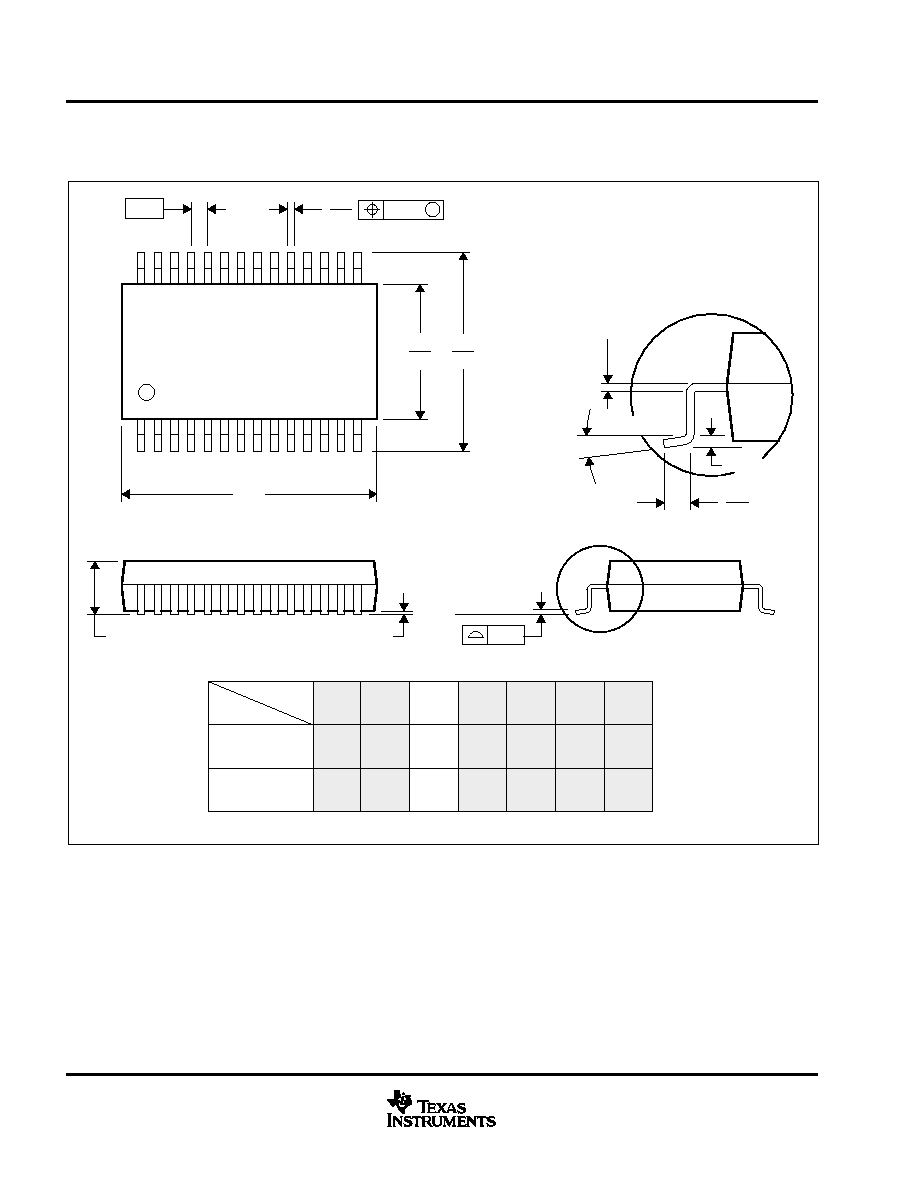
MECHANICAL DATA
DB (R-PDSO-G**)
PLASTIC SMALL-OUTLINE
4040065 /D 09/00
28 PINS SHOWN
Gage Plane
8,20
7,40
0,15 NOM
0,55
0,95
0,25
38
12,90
12,30
28
10,50
24
8,50
Seating Plane
9,90
7,90
30
10,50
9,90
0,38
5,60
5,00
15
0,22
14
A
28
1
20
16
6,50
6,50
14
0,05 MIN
5,90
5,90
DIM
A MAX
A MIN
PINS **
2,00 MAX
6,90
7,50
0,65
M
0,15
0
∞
≠ 8
∞
0,10
NOTES: A. All linear dimensions are in millimeters.
B. This drawing is subject to change without notice.
C. Body dimensions do not include mold flash or protrusion not to exceed 0,15 mm.
D. Falls within JEDEC MO-150

IMPORTANT NOTICE
Texas Instruments Incorporated and its subsidiaries (TI) reserve the right to make corrections, modifications,
enhancements, improvements, and other changes to its products and services at any time and to discontinue
any product or service without notice. Customers should obtain the latest relevant information before placing
orders and should verify that such information is current and complete. All products are sold subject to TI's terms
and conditions of sale supplied at the time of order acknowledgment.
TI warrants performance of its hardware products to the specifications applicable at the time of sale in
accordance with TI's standard warranty. Testing and other quality control techniques are used to the extent TI
deems necessary to support this warranty. Except where mandated by government requirements, testing of all
parameters of each product is not necessarily performed.
TI assumes no liability for applications assistance or customer product design. Customers are responsible for
their products and applications using TI components. To minimize the risks associated with customer products
and applications, customers should provide adequate design and operating safeguards.
TI does not warrant or represent that any license, either express or implied, is granted under any TI patent right,
copyright, mask work right, or other TI intellectual property right relating to any combination, machine, or process
in which TI products or services are used. Information published by TI regarding third≠party products or services
does not constitute a license from TI to use such products or services or a warranty or endorsement thereof.
Use of such information may require a license from a third party under the patents or other intellectual property
of the third party, or a license from TI under the patents or other intellectual property of TI.
Reproduction of information in TI data books or data sheets is permissible only if reproduction is without
alteration and is accompanied by all associated warranties, conditions, limitations, and notices. Reproduction
of this information with alteration is an unfair and deceptive business practice. TI is not responsible or liable for
such altered documentation.
Resale of TI products or services with statements different from or beyond the parameters stated by TI for that
product or service voids all express and any implied warranties for the associated TI product or service and
is an unfair and deceptive business practice. TI is not responsible or liable for any such statements.
Mailing Address:
Texas Instruments
Post Office Box 655303
Dallas, Texas 75265
Copyright
2002, Texas Instruments Incorporated