 | –≠–Ľ–Ķ–ļ—ā—Ä–ĺ–Ĺ–Ĺ—č–Ļ –ļ–ĺ–ľ–Ņ–ĺ–Ĺ–Ķ–Ĺ—ā: OPA2652 | –°–ļ–į—á–į—ā—Ć:  PDF PDF  ZIP ZIP |

FEATURES
q
WIDEBAND BUFFER: 700MHz, G = +1
q
WIDEBAND LINE DRIVER: 200MHz, G = +2
q
HIGH OUTPUT CURRENT: 140mA
q
LOW SUPPLY CURRENT: 5.5mA/Ch
q
ULTRA-SMALL PACKAGE: SOT23-8
q
LOW dG/d
: 0.05%/0.03
į
q
HIGH SLEW RATE: 335V/
Ķ
sec
q
SUPPLY VOLTAGE:
Ī
3V to
Ī
6V
DESCRIPTION
The OPA2652 is a dual, low-cost, wideband voltage-
feedback amplifier intended for price sensitive applica-
tions. It features a high gain bandwidth product of 200MHz
on only 5.5mA/chan quiescent current. Intended for op-
eration on
Ī
5V supplies, it will also support applications
on a single supply from +6V to +12V with 140mA output
current. Its classical differential input, voltage-feedback
design allows wide application in active filters, integra-
tors, transimpedance amplifiers, and differential receiv-
ers.
The OPA2652 is internally compensated for unity gain
stability. It has exceptional bandwidth (700MHz) as a unity
gain buffer, with little peaking (0dB typically). Excellent
DC accuracy is achieved with a low 1.5mV input offset
voltage and 300nA input offset current.
Dual, 700MHz, Voltage-Feedback
OPERATIONAL AMPLIFIER
APPLICATIONS
q
A/D DRIVERS
q
CONSUMER VIDEO
q
ACTIVE FILTERS
q
PULSE DELAY CIRCUITS
q
LOW COST UPGRADE TO THE AD8056
OR EL2210
ģ
OPA2652
TM
RELATED PRODUCTS
SINGLES
DUALS
TRIPLES
QUADS
NOTES
OPA650
OPA2650
--
OPA4650
Ī
5V Spec
OPA680
OPA2680
OPA3680
--
+5V Capable
OPA631
OPA2631
--
--
+3V Capable
OPA634
OPA2634
--
--
+3V Capable
International Airport Industrial Park ∑ Mailing Address: PO Box 11400, Tucson, AZ 85734 ∑ Street Address: 6730 S. Tucson Blvd., Tucson, AZ 85706 ∑ Tel: (520) 746-1111
Twx: 910-952-1111 ∑ Internet: http://www.burr-brown.com/ ∑ Cable: BBRCORP ∑ Telex: 066-6491 ∑ FAX: (520) 889-1510 ∑ Immediate Product Info: (800) 548-6132
For most current data sheet and other product
information, visit www.burr-brown.com
© 2000 Burr-Brown Corporation
PDS-1588B
Printed in U.S.A. June, 2000
OPA2652
Differential ADC Driver
ADS807
12-Bit
53MHz
+In
CM
≠In
+5V
402
+5V
24.9
133
VIN
200
1/2
OPA2652
1/2
OPA2652
22pF
1.00k
0.1
Ķ
F
≠5V
402
24.9
133
200
≠
+
22pF
0.1
Ķ
F
0.1
Ķ
F
1.00k

2
ģ
OPA2652
OPA2652U, E
TYP
GUARANTEED
0
į
C to
≠40
į
C to
MIN/
TEST
PARAMETER
CONDITIONS
+25
į
C
+25
į
C
(2)
70
į
C
(3)
+85
į
C
(3)
UNITS
MAX
LEVEL
(1)
SPECIFICATIONS: V
S
=
Ī
5V
At T
A
= +25
į
C, G = +2, R
F
= 402
, and R
L
= 100
, unless otherwise noted. See Figures 1 and 2 for AC performance only.
AC PERFORMANCE
(Figures 1 and 2)
Small-Signal Bandwidth
G = +1, R
F
= 25
, V
O
= 200mVp-p
700
MHz
typ
C
G = +2, V
O
= 200mVp-p
200
MHz
typ
C
G = +5, V
O
= 200mVp-p
45
MHz
typ
C
Gain Bandwidth Product
G
+10
200
MHz
typ
C
Bandwidth for 0.1dB Flatness
V
O
= 200mVp-p
50
MHz
typ
C
Peaking at a Gain of +1
G = +1, R
F
= 25
,V
O
= 200mVp-p
0
dB
typ
C
Slew Rate
4V Step
335
V/
Ķ
s
typ
C
Rise/Fall Time
200mV Step
2.0
ns
typ
C
4V Step
10
ns
typ
C
Large Signal Bandwidth
V
O
= 4Vp-p
50
MHz
typ
C
SFDR
V
O
= 2Vp-p, 5MHz
66
dB
typ
C
Input Voltage Noise
f > 1MHz
8
nV/
Hz
typ
C
Input Current Noise
f > 1MHz
1.4
pA/
Hz
typ
C
Differential Gain Error
NTSC, R
L
= 150
0.05
%
typ
C
Differential Phase Error
NTSC, R
L
= 150
0.03
degrees
typ
C
Channel-to-Channel Crosstalk
f = 5MHz
≠100
dBc
typ
C
DC PERFORMANCE
(4)
V
CM
= 0V
Open-Loop Voltage Gain
63
56
55
54
dB
min
A
Input Offset Voltage
Ī
1.5
Ī
7
mV
max
A
Average Offset Drift
5
7
Ķ
V/
į
C
max
B
Input Bias Current
4
15
20
25
Ķ
A
max
A
Input Bias Current Drift
Ķ
A/
į
C
max
B
Input Offset Current
Ī
0.3
Ī
1.0
Ī
1.4
Ī
2.0
Ķ
A
max
A
Input Offset Current Drift
Ķ
A/
į
C
max
B
INPUT
(4)
Common-Mode Input Range
Ī
4.0
Ī
3.0
Ī
2.8
Ī
2.7
V
min
A
Common-Mode Rejection Ratio
95
75
dB
min
A
Input Impedance
V
CM
= 0V
Differential
35 || 1
k
|| pF
typ
C
Common Mode
18 || 1
M
|| pF
typ
C
OUTPUT
Voltage Output Swing
1k
Load
Ī
3.0
Ī
2.4
V
min
A
100
Load
Ī
2.5
Ī
2.2
V
min
A
Output Current, Sourcing
V
O
= 0V
140
100
85
75
mA
min
A
Output Current, Sinking
V
O
= 0V
140
100
85
75
mA
min
A
Closed-Loop Output Impedance
f < 100kHz
0.06
typ
C
POWER SUPPLY
Specified Operating Voltage
Ī
5
V
typ
C
Maximum Operating Voltage
Ī
6
Ī
6
Ī
6
V
max
A
Maximum Quiescent Current
Total Both Channels
11
13.2
14
15.5
mA
max
A
Minimum Quiescent Current
Total Both Channels
11
8.8
8
7.5
mA
min
A
Power Supply Rejection Ratio (≠PSRR)
Input Referred
58
54
dB
min
A
THERMAL CHARACTERISTICS
Specified Operating Temperature Range
U, E Package
≠40 to +85
į
C
typ
C
Thermal Resistance,
JA
Junction-to-Ambient
U
SO-8
125
į
C/W
typ
C
E
SOT23-8
150
į
C/W
typ
C
NOTES: (1) Test Levels: (A) 100% tested at 25
į
C. Over temperature limits by characterization and simulation. (B) Limits set by characterization and simulation.
(C) Typical value only for information. (2) Junction temperature = ambient for 25
į
C guaranteed specifications. (3) Junction temperature = ambient at low temperature
limit: junction temperature = ambient +23
į
C at high temperature limit for over temperature guaranteed specifications. (4) Current is considered positive-out-of node.
V
CM
is the input common-mode voltage.

3
ģ
OPA2652
Supply Voltage .................................................................................
Ī
6.5V
Internal Power Dissipation ........................... See Thermal Characteristics
Differential Input Voltage ..................................................................
Ī
1.2V
Input Voltage Range ............................................................................
Ī
V
S
Storage Temperature Range ......................................... ≠40
į
C to +125
į
C
Lead Temperature (SO-8) ............................................................. +260
į
C
Junction Temperature (T
J
) ........................................................... +175
į
C
ESD Rating (Human Body Model) .................................................. 2000V
(Machine Model) ........................................................... 200V
The information provided herein is believed to be reliable; however, BURR-BROWN assumes no responsibility for inaccuracies or omissions. BURR-BROWN assumes no responsibility for the use
of this information, and all use of such information shall be entirely at the user's own risk. Prices and specifications are subject to change without notice. No patent rights or licenses to any of the
circuits described herein are implied or granted to any third party. BURR-BROWN does not authorize or warrant any BURR-BROWN product for use in life support devices and/or systems.
ELECTROSTATIC
DISCHARGE SENSITIVITY
Electrostatic discharge can cause damage ranging from per-
formance degradation to complete device failure. Burr-Brown
Corporation recommends that all integrated circuits be handled
and stored using appropriate ESD protection methods.
ESD damage can range from subtle performance degradation
to complete device failure. Precision integrated circuits may
be more susceptible to damage because very small parametric
changes could cause the device not to meet published speci-
fications.
ABSOLUTE MAXIMUM RATINGS
Top View
SO-8
SOT23-8
PIN CONFIGURATION
PACKAGE/ORDERING INFORMATION
PACKAGE
SPECIFIED
DRAWING
TEMPERATURE
PACKAGE
ORDERING
TRANSPORT
PRODUCT
PACKAGE
NUMBER
RANGE
MARKING
NUMBER
(1)
MEDIA
OPA2652U
SO-8 Surface Mount
182
≠40
į
C to +85
į
C
OPA2652U
OPA2652U
Rails
"
"
"
"
"
OPA2652U/2K5
Tape and Reel
OPA2652E
SOT23-8 Surface Mount
348
≠40
į
C to +85
į
C
C52
OPA2652E/250
Tape and Reel
"
"
"
"
"
OPA2652E/3K
Tape and Reel
NOTE: (1) Models with a slash (/) are available only in Tape and Reel in the quantities indicated (e.g., /3K indicates 3000 devices per reel). Ordering 3000 pieces of
"OPA2652U/3K" will get a single 3000-piece Tape and Reel.
1
2
3
4
8
7
6
5
+V
S
Out B
≠In B
+In B
Out A
≠In A
+In A
≠V
S
OPA2652
C52
Pin 1
SOT23-8 Marking / Pin Orientation

4
ģ
OPA2652
TYPICAL PERFORMANCE CURVES: V
S
=
Ī
5V
At T
A
= +25
į
C, G = +2, R
F
= 402
, and R
L
= 100
, unless otherwise noted. See Figures 1 and 2.
6
3
0
≠3
≠6
≠9
≠12
≠15
≠18
≠21
≠24
NON-INVERTING
SMALL-SIGNAL FREQUENCY RESPONSE
Frequency (Hz)
Normalized Gain (dB)
1M
10M
100M
1G
V
O
= 0.2Vp-p
G = +5
G = +10
G = +1
R
F
= 25
G = +2
6
3
0
≠3
≠6
≠9
≠12
≠15
≠18
≠21
≠24
INVERTING
LARGE-SIGNAL FREQUENCY RESPONSE
Frequency (Hz)
Normalized Gain (dB)
1M
10M
100M
1G
V
O
= 0.5Vp-p
G = ≠1
V
O
= 1.0Vp-p
V
O
= 2.0Vp-p
NON-INVERTING PULSE RESPONSE
Time (5ns/div)
Output Voltage (800mV/div)
Output Voltage (50mV/div)
4Vp-p
G = +2
200mVp-p
INVERTING PULSE RESPONSE
Time (5ns/div)
Output Voltage (800mV/div)
Output Voltage (50mV/div)
4Vp-p
G = ≠1
200mVp-p
6
3
0
≠3
≠6
≠9
≠12
≠15
≠18
≠21
≠24
NON-INVERTING
LARGE-SIGNAL FREQUENCY RESPONSE
Frequency (Hz)
Normalized Gain (dB)
1M
10M
100M
1G
V
O
1Vp-p
G = +2
V
O
= 2Vp-p
V
O
= 4Vp-p
6
3
0
≠3
≠6
≠9
≠12
≠15
≠18
≠21
≠24
INVERTING
SMALL-SIGNAL FREQUENCY RESPONSE
Frequency (Hz)
Normalized Gain (dB)
1M
10M
100M
1G
V
O
= 0.2Vp-p
G = ≠5
G = ≠10
G = ≠1
G = ≠2

5
ģ
OPA2652
TYPICAL PERFORMANCE CURVES: V
S
=
Ī
5V
(Cont.)
At T
A
= +25
į
C, G = +2, R
F
= 402
, and R
L
= 100
, unless otherwise noted. See Figures 1 and 2.
≠50
≠60
≠70
≠80
≠90
HARMONIC DISTORTION vs FREQUENCY
Frequency (MHz)
0.1
1
10
20
Harmonic Distortion (dBc)
V
O
= 2Vp-p
3rd Harmonic
2nd Harmonic
≠50
≠60
≠70
≠80
≠90
HARMONIC DISTORTION vs LOAD RESISTANCE
R
L
(
)
100
1000
Harmonic Distortion (dBc)
V
O
= 2Vp-p
f = 5MHz
3rd Harmonic
2nd Harmonic
≠50
≠60
≠70
≠80
≠90
HARMONIC DISTORTION vs SUPPLY VOLTAGE
Supply Voltage (V)
Ī
3
Ī
4
Ī
5
Ī
6
Harmonic Distortion (dBc)
V
O
= 2Vp-p
f
= 5MHz
3rd Harmonic
2nd Harmonic
≠50
≠60
≠70
≠80
≠90
HARMONIC DISTORTION vs NON-INVERTING GAIN
Gain Magnitude (V/V)
Harmonic Distortion (dBc)
1
10
V
O
= 2Vp-p
f = 5MHz
2nd Harmonic
3rd Harmonic
≠50
≠60
≠70
≠80
≠90
HARMONIC DISTORTION vs INVERTING GAIN
Gain Magnitude (V/V)
Harmonic Distortion (dBc)
1
10
V
O
= 2Vp-p
f = 5MHz
2nd Harmonic
3rd Harmonic
≠50
≠60
≠70
≠80
≠90
HARMONIC DISTORTION vs OUTPUT VOLTAGE
Output Voltage (Vp-p)
Harmonic Distortion (dBc)
0.1
1
4
f = 5MHz
3rd Harmonic
2nd Harmonic

6
ģ
OPA2652
TYPICAL PERFORMANCE CURVES: V
S
=
Ī
5V
(Cont.)
At T
A
= +25
į
C, G = +2, R
F
= 402
, and R
L
= 100
, unless otherwise noted. See Figures 1 and 2.
2
1
0
≠1
≠2
≠3
≠4
≠5
≠6
≠7
≠8
FREQUENCY RESPONSE vs CAPACITIVE LOAD
Frequency (Hz)
0
1G
10M
100M
Normalized Gain to Capacitive Load (dB)
G = +2
1/2
OPA2652
R
S
V
O
C
L
1k
C
L
= 10pF
C
L
= 22pF
C
L
= 47pF
C
L
= 100pF
≠50
≠60
≠70
≠80
≠90
TWO-TONE, 3rd-ORDER SPURIOUS LEVEL
Single-Tone Load Power (dBm)
≠8
≠6
≠4
≠2
0
2
4
3rd-Order Spurious Level (dBc)
1MHz
2MHz
20MHz
10MHz
5MHz
Load Power at matched 50
load
0.30
0.25
0.20
0.15
0.10
0.05
0.00
COMPOSITE VIDEO dG/d
Number of 150
Loads
1
2
3
4
dG/d
(%
/
į
)
d
, Positive Video
d
, Negative Video
dG, Positive Video
dG, Negative Video
100
10
1
INPUT VOLTAGE AND CURRENT NOISE DENSITY
Frequency (Hz)
100
1k
10k
100k
1M
10M
Voltage Noise (nV/
Hz)
Current Noise (pA/
Hz)
Voltage Noise = 8.0nV/
Hz
Current Noise = 1.4pA/
Hz
70
60
50
40
30
20
10
0
RECOMMENDED R
S
vs CAPACITIVE LOAD
Capacitive Load (pF)
1
10
100
1000
R
S
(
)
≠30
≠40
≠50
≠60
≠70
≠80
≠90
CHANNEL-TO-CHANNEL CROSSTALK
Frequency (MHz)
10
100
1000
Crosstalk, Input-Referred (dB)

7
ģ
OPA2652
TYPICAL PERFORMANCE CURVES: V
S
=
Ī
5V
(Cont.)
At T
A
= +25
į
C, G = +2, R
F
= 402
, and R
L
= 100
, unless otherwise noted. See Figures 1 and 2.
5
4
3
2
1
0
≠1
≠2
≠3
≠4
≠5
OUTPUT VOLTAGE AND CURRENT LIMITATIONS
I
O
(mA)
≠200
≠150
≠100
≠50
0
100
50
150
200
V
O
(V)
Output Current Limited
1W Internal
Power Limit
1W Internal
Power Limit
Output Current Limit
20
Load Line
10
Load Line
50
Load Line
100
Load Line
5
4
3
2
1
0
≠1
≠2
≠3
≠4
≠5
INVERTING OVERDRIVE RECOVERY
V
IN
Time (20ns/div)
Input and Output Voltage (V)
V
OUT
G = ≠1
100
10
1
0.1
0.01
CLOSED-LOOP OUTPUT IMPEDANCE vs FREQUENCY
Frequency (Hz)
10k
400M
100k
1M
100M
10M
Output Impedance (
)
1/2
OPA2652
402
200
402
Z
O
5
4
3
2
1
0
≠1
≠2
≠3
≠4
≠5
NON-INVERTING OVERDRIVE RECOVERY
V
IN
Time (20ns/div)
Output Voltage (V)
2.5
2.0
1.5
1.0
0
0.50
≠0.5
≠1.0
≠2.0
≠2.5
Input Voltage (V)
V
OUT
G = +2
100
90
80
70
60
50
40
30
20
10
0
CMRR AND PSRR vs FREQUENCY
Frequency (Hz)
1k
100M
10k
100k
1M
10M
Power Supply Rejection Ratio (dB)
Common-Mode Rejection Ratio (dB)
CMRR
+PSRR
≠PSRR
70
60
50
40
30
20
10
0
≠10
0
≠30
≠60
≠90
≠120
≠150
≠180
≠210
≠240
OPEN-LOOP GAIN AND PHASE
Frequency (Hz)
10k
1G
100k
10M
1M
100M
Open-Loop Gain (dB)
Open-Loop Phase (
į
)
Open-Loop Gain
Open-Loop Phase

8
ģ
OPA2652
TYPICAL PERFORMANCE CURVES: V
S
=
Ī
5V
(Cont.)
At T
A
= +25
į
C, G = +2, R
F
= 402
, and R
L
= 100
, unless otherwise noted. See Figures 1 and 2.
6
5
4
3
2
1
0
≠1
≠2
≠3
≠4
≠5
≠6
TYPICAL DC DRIFT OVER TEMPERATURE
Ambient Temperature (
į
C)
≠40
≠20
0
20
40
60
80
100
Input Offset Voltage (mV)
Input Bias and Offset Current (
Ķ
A)
I
OS
V
OS
I
B
6
5
4
3
2
1
0
COMMON-MODE INPUT VOLTAGE RANGE
AND OUTPUT SWING vs SUPPLY VOLTAGE
Supply Voltage (V)
Ī
3
Ī
4
Ī
5
Ī
6
Voltage Range (V)
Positive Common-Mode Input Range
Negative Output Voltage Range
Positive Output Voltage Range
Negative Common-Mode Input Range
250
200
150
100
50
0
25
20
15
10
5
0
SUPPLY AND OUTPUT CURRENT vs TEMPERATURE
Ambient Temperature (
į
C)
≠40
≠20
0
20
40
60
80
100
Output Current (mA)
Supply Current (mA)
Sourcing Output Current
Quiescent Supply Current
(Both Channels)
Sinking Output Current

9
ģ
OPA2652
APPLICATIONS INFORMATION
WIDEBAND VOLTAGE FEEDBACK OPERATION
The OPA2652 is a dual low power, wideband voltage
feedback operational amplifier. Each channel is internally
compensated to provide unity gain stability. The OPA2652's
voltage feedback architecture features true differential and
fully symmetrical inputs. This minimizes offset errors, mak-
ing the OPA2652 well suited for implementing filter and
instrumentation designs. As a dual operational amplifier,
OPA2652 is an ideal choice for designs requiring multiple
channels where reduction of board space, power dissipation
and cost are critical. Its AC performance is optimized to
provide a gain bandwidth product of 200MHz and a fast rise
time of 2.0ns, which is an important consideration in high
speed data conversion applications. The low DC input offset
of
Ī
1.5mV and drift of
Ī
5
Ķ
V/
į
C support high accuracy
requirements. In applications requiring a higher slew rate
and wider bandwidth, such as video and high bit rate digital
communications, consider the dual current feedback
OPA2658, or OPA2681.
Figure 1 shows the DC-coupled, gain of +2, dual power
supply circuit configuration used as the basis of the
Ī
5V
Specifications and Typical Performance Curves. This is for
one channel. The other channel is connected similarly. For
test purposes, the input impedance is set to 50
with a
resistor to ground and the output impedance is set to 50
with a series output resistor. Voltage swings reported in the
specifications are taken directly at the input and output pins,
while output powers (dBm) are at the matched 50
load. For
the circuit of Figure 1, the total effective load will be 100
|| 804
. Two optional components are included in Figure 1.
An additional resistor (174
) is included in series with the
non-inverting input. Combined with the 25
DC source
resistance looking back towards the signal generator, this
gives an input bias current cancelling resistance that matches
the 201
source resistance seen at the inverting input (see the
DC Accuracy and Offset Control section). In addition to the
usual power supply decoupling capacitors to ground, a 0.1
Ķ
F
capacitor is included between the two power supply pins. In
practical PC board layouts, this optional-added capacitor will
typically improve the 2nd harmonic distortion performance
by 3dB to 6dB.
Figure 2 shows the DC-coupled gain of ≠1, bipolar supply
circuit configuration which is the basis of the Specifications
and Typical Performance Curves at G = ≠1. The input
impedance matching resistor (57.6
) used for testing gives a
50
input load. A resistor (205
) connects the non-inverting
input to ground. This provides the DC source resistance
matching to cancel outputs errors due to input bias current.
1/2
OPA2652
+5V
+
≠5V
50
Load
49.9
174
49.9
V
O
V
I
50
Source
R
G
402
R
F
402
+
6.8
Ķ
F
0.1
Ķ
F
6.8
Ķ
F
0.1
Ķ
F
0.1
Ķ
F
FIGURE 1. DC-Coupled, G = +2, Bipolar Supply, Specifi-
cation and Test Circuit.
FIGURE 2. DC-Coupled, G = ≠1, Bipolar Supply, Specifi-
cation and Test Circuit.
1/2
OPA2652
50
R
F
402
R
G
402
R
B
205
R
M
57.6
Source
+5V
≠5V
R
O
49.9
0.1
Ķ
F
6.8
Ķ
F
+
0.1
Ķ
F
0.1
Ķ
F
6.8
Ķ
F
+
50
Load
V
O
V
I
= ≠1
V
O
V
I
DIFFERENTIAL ADC DRIVER
The circuit on the front page shows an OPA2652 driving the
ADS807 A/D converter differentially, at a gain of +2V/V.
The outputs are AC-coupled to the converter to adjust for the
difference in supply voltages. The 133
resistors at the non-
inverting inputs minimize DC offset errors. The differential
topology minimizes even-order distortion products, such as
second-harmonic distortion.

10
ģ
OPA2652
BANDPASS FILTER
Figure 3 shows a single OPA2652 implementing a sixth-
order bandpass filter. This filter cascades two second-order
Sallen-Key sections with transmission zeros, and a double
real pole section. It has 0.3dB of ripple, ≠3dB frequencies of
450kHz and 11MHz, and ≠23dB frequencies of 315kHz and
16MHz. The 20.0
resistor isolates the first OPA2652 out-
put from capacitive loading. This improves stability with
minimal impact on the filter response. Figure 4 shows the
nominal response simulated by SPICE.
0
≠5
≠10
≠15
≠20
≠25
≠30
≠35
≠40
10k
100k
1M
10M
100M
Gain (dB)
Frequency (Hz)
1/2
OPA2652
402
402
Video
Input
Video
Output
+5V
≠5V
75.0
75.0
1/2
OPA2652
24.9
143
140
2.10k
1.0nF
1.0nF
V
IN
+5V
≠5V
2.2nF
1.30k
1/2
OPA2652
24.9
200
107
225
20.0
158
150pF
12pF
2.7nF
+5V
≠5V
180pF
100
100pF
1% Resistors
5% Capacitors
18pF
V
OUT
VIDEO LINE DRIVER
Figure 5 shows the OPA2652 used as a video line driver. Its
outstanding differential gain and phase allow it to be used in
studio equipment, while its low cost and SOT23-8 package
option will support consumer applications.
PULSE DELAY CIRCUIT
Figure 6 shows the OPA2652 used in a pulse delay circuit.
This circuit cascades the two op amps in the OPA2652, each
forming a single pole, active allpass filter. The overall gain
is +1, and the overall delay through the filter is:
t
GD
= n(2RC), overall group delay
n= 2, the number of cascaded stages
FIGURE 4. Nominal Filter Response.
FIGURE 3. Bandpass Filter.
FIGURE 5. Video Line Driver.

11
ģ
OPA2652
R
F
and R
G
need to be equal to maintain a constant gain
magnitude. The rise and fall times of the input pulses (t
r(IN)
)
should be slow enough to prevent pre-shoot artifacts in the
response.
t
r (IN)
5RC, minimal pre-shoot
SIMPLE BANDPASS FILTER
Figure 7 shows the OPA2652 used as simple bandpass filter.
The OPA2652 is well suited for this type of circuit because
it is very stable at a noise gain of +1.
MACROMODELS AND APPLICATIONS SUPPORT
Computer simulation of circuit performance using SPICE is
often useful when analyzing the performance of analog
circuits and systems. This is particularly true for Video and
RF amplifier circuits where parasitic capacitance and induc-
tance can have a major effect on circuit performance. Check
the Burr-Brown web site (www.burr-brown.com) for avail-
able SPICE products (not all parts have models). These
models do a good job of predicting small-signal AC and
transient performance under a wide variety of operating
conditions. They do not do as well in predicting the har-
monic distortion or dG/d
characteristics. These models do
not attempt to distinguish between the package types in their
small-signal AC performance.
OPERATING SUGGESTIONS
OPTIMIZING RESISTOR VALUES
Since the OPA2652 is a unity gain stable voltage feedback
op amp, a wide range of resistor values may be used for the
feedback and gain setting resistors. The primary limits on
these values are set by dynamic range (noise and distortion)
and parasitic capacitance considerations. For a non-inverting
unity gain follower application, the feedback connection
should be made with a 25
resistor, not a direct short. This
will isolate the inverting input capacitance from the output
pin and improve the frequency response flatness. Usually,
the feedback resistor value should be between 200
and
1.5k
. Below 200
, the feedback network will present
additional output loading which can degrade the harmonic
distortion performance of the OPA2652. Above 1.5k
, the
typical parasitic capacitance (approximately 0.2pF) across
the feedback resistor may cause unintentional band-limiting
in the amplifier response.
A good rule of thumb is to target the parallel combination of
R
F
and R
G
(Figure 1) to be less than approximately 300
.
The combined impedance R
F
|| R
G
interacts with the invert-
ing input capacitance, placing an additional pole in the
feedback network, and thus a zero in the forward response.
Assuming a 2pF total parasitic on the inverting node, hold-
ing R
F
|| R
G
< 300
will keep this pole above 250MHz. By
itself, this constraint implies that the feedback resistor R
F
can increase to several k
at high gains. This is acceptable
as long as the pole formed by R
F
and any parasitic capaci-
tance appearing in parallel is kept out of the frequency range
of interest.
1/2
OPA2652
402
C
R
402
1/2
OPA2652
R
G
402
R
F
402
C
V
O
V
IN
+5V
≠5V
+5V
≠5V
R
V
OUT
V
IN
+5V
≠5V
C
2
C
1
402
402
402
1/2
OPA2652
DESIGN-IN TOOLS
DEMONSTRATION BOARDS
PC boards are available to assist in the initial evaluation of
circuit performance using the OPA2652. They are available
free as unpopulated PC boards delivered with descriptive
documentation. The summary information for these boards is
shown below:
FIGURE 6. Pulse Delay Circuit.
FIGURE 7. Inverting Bandpass Filter.
BOARD
PART
ORDERING
PRODUCT
PACKAGE
NUMBER
NUMBER
OPA2652U
8-Lead SO-8
DEM-OPA26xU
MKT-352
OPA2652E
SOT23-8
DEM-OPA2652E
MKT-365
Contact the Burr-Brown Applications support line to request
this board.

12
ģ
OPA2652
BANDWIDTH VS GAIN: NON-INVERTING OPERATION
Voltage feedback op amps exhibit decreasing closed-loop
bandwidth as the signal gain is increased. In theory, this
relationship is described by the Gain Bandwidth Product
(GBP) shown in the specifications. Ideally, dividing GBP by
the non-inverting signal gain (also called the Noise Gain, or
NG) will predict the closed-loop bandwidth. In practice, this
only holds true when the phase margin approaches 90
į
, as it
does in high gain configurations. At low gains (increased
feedback factor), most amplifiers will exhibit a wider band-
width and lower phase margin. The OPA2652 is compen-
sated to give a flat response in a non-inverting gain of 1
(Figure 1). This results in a typical gain of +1 bandwidth of
700MHz, far exceeding that predicted by dividing the
200MHz GBP by NG = 1. Increasing the gain will cause the
phase margin to approach 90
į
and the bandwidth to more
closely approach the predicted value of (GBP/NG). At a gain
of +5, the 45MHz bandwidth shown in the Typical Specifi-
cations is close to that predicted using this simple formula.
INVERTING AMPLIFIER OPERATION
Since the OPA2652 is a general purpose, wideband volt-
age feedback op amp, all of the familiar op amp applica-
tion circuits are available to the designer. Inverting opera-
tion is one of the more common requirements and offers
several performance benefits. Figure 2 shows a typical
inverting configuration.
In the inverting configuration, three key design consider-
ation must be noted. The first is that the gain resistor (R
G
)
becomes part of the signal channel input impedance. If input
impedance matching is desired (which is beneficial when-
ever the signal is coupled through a cable, twisted pair, long
PC board trace or other transmission line conductor), R
G
may be set equal to the required termination value and R
F
adjusted to give the desired gain. This is the simplest
approach and results in optimum bandwidth and noise per-
formance. However, at low inverting gains, the resultant
feedback resistor value can present a significant load to the
amplifier output. For an inverting gain of ≠1, setting R
G
to
50
for input matching eliminates the need for R
M
but
requires a 50
feedback resistor. This has the interesting
advantage that the noise gain becomes equal to 2 for a 50
source impedance--the same as the non-inverting circuits
considered above. However, the amplifier output will now
see the 50
feedback resistor in parallel with the external
load. In general, the feedback resistor should be limited to
the 200
to 1.5k
range. In this case, it is preferable to
increase both the R
F
and R
G
values as shown in Figure 2, and
then achieve the input matching impedance with a third
resistor (R
M
) to ground. The total input impedance becomes
the parallel combination of R
G
and R
M
.
The second major consideration, touched on in the previous
paragraph, is that the signal source impedance becomes part
of the noise gain equation and influences the bandwidth. For
the example in Figure 2, the R
M
value combines in parallel
with the external 50
source impedance, yielding an effec-
tive driving impedance of 50
|| 57.6
= 26.8
. This
impedance is added in series with R
G
for calculating the noise
gain (NG). The resultant NG is 1.94 for Figure 2, (an ideal 0
source would cause NG = 2.00).
The third important consideration in inverting amplifier
design is setting the bias current cancellation resistor on the
non-inverting input (R
B
). If this resistor is set equal to the
total DC resistance looking out of the inverting node, the
output DC error, due to the input bias currents, will be
reduced to (Input Offset Current) ∑ R
F
. If the 50
source
impedance is DC-coupled in Figure 2, the total resistance to
ground on the inverting input will be 429
. Combining this
in parallel with the feedback resistor gives 208
, which is
close to the R
B
= 205
used in Figure 2. To reduce the
additional high frequency noise introduced by this resistor,
it is sometimes bypassed with a capacitor. As long as R
B
<300
, the capacitor is not required since its total noise
contribution will be much less than that of the op amp's
input noise voltage.
OUTPUT CURRENT AND VOLTAGE
The OPA2652 specifications in the spec table, though famil-
iar in the industry, consider voltage and current limits sepa-
rately. In many applications, it is the voltage ∑ current, or V-
I product, which is more relevant to circuit operation. Refer
to the "Output Voltage and Current Limitations" plot in the
Typical Performance Curves. The X and Y axes of this graph
show the zero-voltage output current limit and the zero-
current output voltage limit, respectively. The four quadrants
give a more detailed view of the OPA2652's output drive
capabilities, noting that the graph is bounded by a "Safe
Operating Area" of 1W maximum internal power dissipation
(500mW for each channel). Superimposing resistor load
lines onto the plot shows that the OPA2652 can drive
Ī
2.2V
into 50
or
Ī
2.5V into 100
without exceeding the output
capabilities, or the 1W dissipation boundary line.
To maintain maximum output stage linearity, no output
short-circuit protection is provided. This will not normally
be a problem since most applications include a series match-
ing resistor at the output that will limit the internal power
dissipation if the output side of this resistor is shorted to
ground. However, shorting the output pin directly to the
adjacent positive power supply pin will, in most cases,
destroy the amplifier. Including a small series resistor (5
)
in the power supply line will protect against this. Always
place the 0.1
Ķ
F decoupling capacitor directly on the supply
pins.
DRIVING CAPACITIVE LOADS
One of the most demanding and yet very common load
conditions for an op amp is capacitive loading. Often, the
capacitive load is the input of an A/D converter--including
additional external capacitance which may be recommended
to improve A/D linearity. A high speed amplifier like the
OPA2652 can be very susceptible to decreased stability and
closed-loop response peaking when a capacitive load is
13
ģ
OPA2652
placed directly on the output pin. When the amplifier's
open-loop output resistance is considered, this capacitive
load introduces an additional pole in the signal path that can
decrease the phase margin. Several external solutions to this
problem have been suggested. When the primary consider-
ations are frequency response flatness, pulse response fidel-
ity and/or distortion, the simplest and most effective solution
is to isolate the capacitive load from the feedback loop by
inserting a series isolation resistor between the amplifier
output and the capacitive load. This does not eliminate the
pole from the loop response, but rather shifts it and adds a
zero at a higher frequency. The additional zero acts to cancel
the phase lag from the capacitive load pole, thus increasing
the phase margin and improving stability.
The Typical Performance Curves show the recommended
R
S
versus capacitive load and the resulting frequency re-
sponse at the load. Parasitic capacitive loads greater than
2pF can begin to degrade the performance of the OPA2652.
Long PC board traces, unmatched cables, and connections to
multiple devices can easily exceed this value. Always con-
sider this effect carefully, and add the recommended series
resistor as close as possible to the OPA2652 output pin (see
Board Layout Guidelines).
DISTORTION PERFORMANCE
The OPA2652 provides good distortion performance into a
100
load on
Ī
5V supplies. Increasing the load impedance
improves distortion directly. Remember that the total load
includes the feedback network; in the non-inverting configu-
ration (Figure 1) this is sum of R
F
+ R
G
, while in the
inverting configuration, it is just R
F
. Also, providing an
additional supply decoupling capacitor (0.1
Ķ
F) between the
supply pins (for bipolar operation) improves the 2nd-order
distortion slightly (3dB to 6dB).
It is also true that increasing the output voltage swing
increases harmonic distortion.
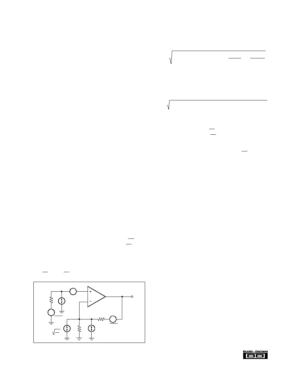
NOISE PERFORMANCE
The OPA2652 input-referred voltage noise (8nV/
Hz), and
the two input-referred current noise terms (1.4pA/
Hz), com-
bine to give low output noise under a wide variety of operating
conditions. Figure 8 shows the op amp noise analysis model
with all the noise terms included. In this model, all noise terms
are taken to be noise voltage or current density terms in either
nV/
Hz or pA/
Hz.
The total output spot noise voltage can be computed as the
square root of the sum of all squared output noise voltage
contributors. Equation 1 shows the general form for the
output noise voltage using the terms shown in Figure 10.
Equation 1:
Dividing this expression by the noise gain (NG = 1+R
F
/R
G
)
will give the equivalent input-referred spot noise voltage at
the non-inverting input, as shown in Equation 2.
Equation 2:
Evaluating these two equations for the OPA2652 circuit and
component values shown in Figure 1 will give a total output
spot noise voltage of 17nV/
Hz and a total equivalent input
spot noise voltage of 8.4nV/
Hz. This is including the noise
added by the bias current cancellation resistor (205
) on the
non-inverting input. This total input-referred spot noise
voltage is only slightly higher than the 8nV/
Hz specifica-
tion for the op amp voltage noise alone. This will be the case
as long as the impedances appearing at each op amp input
are limited to the previously recommend maximum value of
300
. Keeping both (R
F
|| R
G
) and the non-inverting input
source impedance less than 300
will satisfy both noise and
frequency response flatness considerations. Since the resis-
tor-induced noise is relatively negligible, additional capaci-
tive decoupling across the bias current cancellation resistor
(R
B
) for the inverting op amp configuration of Figure 2 is not
required.
DC ACCURACY AND OFFSET CONTROL
The balanced input stage of a wideband voltage feedback op
amp allows good output DC accuracy in a wide variety of
applications. Although the high speed input stage does
require relatively high input bias current (typically 4
Ķ
A out
of each input terminal), the close matching between them
may be used to significantly reduce the output DC error
caused by this current. This is done by matching the DC
source resistances appearing at the two inputs. This reduces
the output DC error due to the input bias currents to the
offset current times the feedback resistor. Evaluating the
configuration of Figure 1, using worst-case +25
į
C input
offset voltage and current specifications, gives a worst-case
output offset voltage equal to:
Ī
(NG ∑ V
OS(MAX)
)
Ī
(R
F
∑ I
OS(MAX)
)
=
Ī
(1.94 ∑ 7.0mV)
Ī
(402
∑ 1.0
Ķ
A)
=
Ī
14.0mV
(NG = non-inverting signal gain)
A fine scale output offset null, or DC operating point
adjustment, is often required. Numerous techniques are
available for introducing DC offset control into an op amp
E
N
=
E
NI
2
+
I
BN
R
S
(
)
2
+ 4
kTR
S
+
I
BI
R
F
NG
2
+ 4
kTR
F
NG
E
O
=
E
NI
2
+
I
BN
R
S
(
)
2
+ 4
kTR
S
(
)
NG
2
+
I
BI
R
F
(
)
2
+ 4
kTR
F
NG
4kT
R
G
R
G
R
F
R
S
1/2
OPA2652
I
BI
E
O
I
BN
4kT = 1.6x10
≠20
J
at 290
į
K
E
RS
E
NI
4kTR
S
4kTR
F
FIGURE 8. Op Amp Noise Analysis Model.

14
ģ
OPA2652
circuit. Most of these techniques add a DC current through
the feedback resistor. In selecting an offset trim method, one
key consideration is the impact on the desired signal path
frequency response. If the signal path is intended to be non-
inverting, the offset control is best applied as an inverting
summing signal to avoid interaction with the signal source.
If the signal path is intended to be inverting, applying the
offset control to the non-inverting input may be considered.
However, the DC offset voltage on the summing junction
will set up a DC current back into the source which must be
considered. Applying an offset adjustment to the inverting
op amp input can change the noise gain and frequency
response flatness. For a DC-coupled inverting amplifier,
Figure 9 shows one example of an offset adjustment tech-
nique that has minimal impact on the signal frequency
response. In this case, the DC offset current is brought into
the inverting input node through resistor values that are
much larger than the signal path resistors. This will insure
that the adjustment circuit has minimal effect on the loop
gain and hence the frequency response.
Note that it is the power in the output stage, and not into the
load, that determines internal power dissipation.
As an example, compute the maximum T
J
using an
OPA2652E (SOT23-8 package) in the circuit of Figure 1
operating at the maximum specified ambient temperature of
+85
į
C and with both outputs driving 2.5V
DC
into a grounded
100
load.
P
D
= 10V ∑ 15.5mA + 2 [5
2
/(4∑(100
|| 804
))] = 296mW
Maximum T
J
= +85
į
C + (0.30W ∑ 150
į
C/W) = 130
į
C.
This absolute worst-case condition meets the specified maxi-
mum junction temperature. Actual P
DL
will almost always
be less than that considered here. Carefully consider maxi-
mum T
J
in your application.
BOARD LAYOUT GUIDELINES
Achieving optimum performance with a high frequency
amplifier like the OPA2652 requires careful attention to
board layout parasitics and external component types. Rec-
ommendations that will optimize performance include:
a) Minimize parasitic capacitance to any AC ground for all
of the signal I/O pins. Parasitic capacitance on the output
and inverting input pins can cause instability: on the non-
inverting input, it can react with the source impedance to
cause unintentional bandlimiting. To reduce unwanted ca-
pacitance, a window around the signal I/O pins should be
opened in all of the ground and power planes around those
pins. Otherwise, ground and power planes should be unbro-
ken elsewhere on the board.
b) Minimize the distance (<0.25") from the power supply
pins to high frequency 0.1
Ķ
F decoupling capacitors. At the
device pins, the ground and power plane layout should not
be in close proximity to the signal I/O pins. Avoid narrow
power and ground traces to minimize inductance between
the pins and the decoupling capacitors. The power supply
connections should always be decoupled with these capaci-
tors. An optional supply decoupling capacitor (0.1
Ķ
F) across
the two power supplies (for bipolar operation) will improve
2nd harmonic distortion performance. Larger (2.2
Ķ
F to
6.8
Ķ
F) decoupling capacitors, effective at lower frequency,
should also be used on the main supply pins. These may be
placed somewhat farther from the device and may be shared
among several devices in the same area of the PC board.
c) Careful selection and placement of external compo-
nents will preserve the high frequency performance of
the OPA2652. Resistors should be a very low reactance
type. Surface-mount resistors work best and allow a tighter
overall layout. Metal film or carbon composition axially-
leaded resistors can also provide good high frequency per-
formance. Again, keep their leads and PC board traces as
short as possible. Never use wirewound type resistors in a
high frequency application. Since the output pin and invert-
ing input pin are the most sensitive to parasitic capacitance,
always position the feedback and series output resistor, if
FIGURE 9. DC-Coupled, Inverting Gain of ≠2, with Offset
Adjustment.
R
F
1k
Ī
200mV Output Adjustment
= ≠ = ≠2
Supply Decoupling
Not Shown
5k
5k
328
0.1
Ķ
F
R
G
500
V
I
20k
10k
0.1
Ķ
F
≠5V
+5V
1/2
OPA2652
+5V
≠5V
V
O
V
O
V
I
R
F
R
G
THERMAL ANALYSIS
Heatsinking or forced airflow may be required under ex-
treme operating conditions. Maximum desired junction tem-
perature will set the maximum allowed internal power dis-
sipation as described below. In no case should the maximum
junction temperature be allowed to exceed 175
į
C.
Operating junction temperature (T
J
) is given by T
A
+ P
D
∑
JA
.
The total internal power dissipation (P
D
) is the sum of
quiescent power (P
DQ
) and additional power dissipated in
the output stage (P
DL
) to deliver load power. Quiescent
power is simply the specified no-load supply current times
the total supply voltage across the part. P
DL
will depend on
the required output signal and load but would, for a grounded
resistive load, be at a maximum when the output is fixed at
a voltage equal to 1/2 of either supply voltage (for equal
bipolar supplies). Under this condition, P
DL
= V
S
2
/(4∑R
L
)
where R
L
includes feedback network loading.

15
ģ
OPA2652
any, as close as possible to the output pin. Other network
components, such as non-inverting input termination resis-
tors, should also be placed close to the package. Where
double-side component mounting is allowed, place the feed-
back resistor directly under the package on the other side of
the board between the output and inverting input pins. Even
with a low parasitic capacitance shunting the external resis-
tors, excessively high resistor values can create significant
time constants that can degrade performance. Good axial
metal film or surface-mount resistors have approximately
0.2pF in shunt with the resistor. For resistor values >1.5k
,
this parasitic capacitance can add a pole and/or zero below
500MHz that can effect circuit operation. Keep resistor
values as low as possible consistent with load driving con-
siderations. The 402
feedback used in the typical perfor-
mance specifications is a good starting point for design.
Note that a 25
feedback resistor, rather than a direct short,
is suggested for the unity gain follower application. This
effectively isolates the inverting input capacitance from the
output pin that would otherwise cause additional peaking in
the gain of +1 frequency response.
d) Connections to other wideband devices on the board
may be made with short direct traces or through on-board
transmission lines. For short connections, consider the trace
and the input to the next device as a lumped capacitive load.
Relatively wide traces (50 to 100mils) should be used,
preferably with ground and power planes opened up around
them. Estimate the total capacitive load and set R
S
from the
plot of Recommended R
S
vs Capacitive Load. Low parasitic
capacitive loads (<5pF) may not need an R
S
since the
OPA2652 is nominally compensated to operate with a 2pF
parasitic load. Higher parasitic capacitive loads without an
R
S
are allowed as the signal gain increases (increasing the
unloaded phase margin) If a long trace is required, and the
6dB signal loss intrinsic to a doubly terminated transmission
line is acceptable, implement a matched impedance trans-
mission line using microstrip or stripline techniques (consult
an ECL design handbook for microstrip and stripline layout
techniques). A 50
environment is normally not necessary
on board, and in fact, a higher impedance environment will
improve distortion as shown in the distortion versus load
plots. With a characteristic board trace impedance defined
(based on board material and trace dimensions), a matching
series resistor into the trace from the output of the OPA2652
is used as well as a terminating shunt resistor at the input of
the destination device. Remember also that the terminating
impedance will be the parallel combination of the shunt
resistor and the input impedance of the destination device;
this total effective impedance should be set to match the
trace impedance. The high output voltage and current capa-
bility of the OPA2652 allows multiple destination devices to
be handled as separate transmission lines, each with their
own series and shunt terminations. If the 6dB attenuation of
a doubly terminated transmission line is unacceptable, a
long trace can be series-terminated at the source end only.
Treat the trace as a capacitive load in this case and set the
series resistor value as shown in the plot of Recommended
R
S
vs Capacitive Load. This will not preserve signal integ-
rity as well as a doubly terminated line. If the input imped-
ance of the destination device is low, there will be some
signal attenuation due to the voltage divider formed by the
series output into the terminating impedance.
e) Socketing a high speed part like the OPA2652 is not
recommended. The additional lead length and pin-to-pin
capacitance introduced by the socket can create an ex-
tremely troublesome parasitic network which can make it
almost impossible to achieve a smooth, stable frequency
response. Best results are obtained by soldering the OPA2652
onto the board.
INPUT AND ESD PROTECTION
The OPA2652 is built using a very high speed complemen-
tary bipolar process. The internal junction breakdown volt-
ages are relatively low for these very small geometry de-
vices. These breakdowns are reflected in the "Absolute
Maximum Ratings" table. All device pins are protected with
internal ESD protection diodes to the power supplies as
shown in Figure 10.
These diodes provide moderate protection to input overdrive
voltages above the supplies as well. The protection diodes
can typically support 30mA continuous current. Where higher
currents are possible (e.g., in systems with
Ī
15V supply
parts driving into the OPA2652), current-limiting series
resistors should be added into the two inputs. Keep these
resistor values as low as possible since high values degrade
both noise performance and frequency response.
External
Pin
+V
CC
≠V
CC
Internal
Circuitry
FIGURE 10. Internal ESD Protection.