 | ÐлекÑÑоннÑй компоненÑ: DS821E | СкаÑаÑÑ:  PDF PDF  ZIP ZIP |
ADS821
ADS821U
ADS821E
TM
ADS821
®
FEATURES
q
NO MISSING CODES
q
INTERNAL REFERENCE
q
LOW POWER: 380mW
q
HIGH SNR: 58dB
q
INTERNAL TRACK/HOLD
q
PACKAGE: 28-Pin SOIC and SSOP
DESCRIPTION
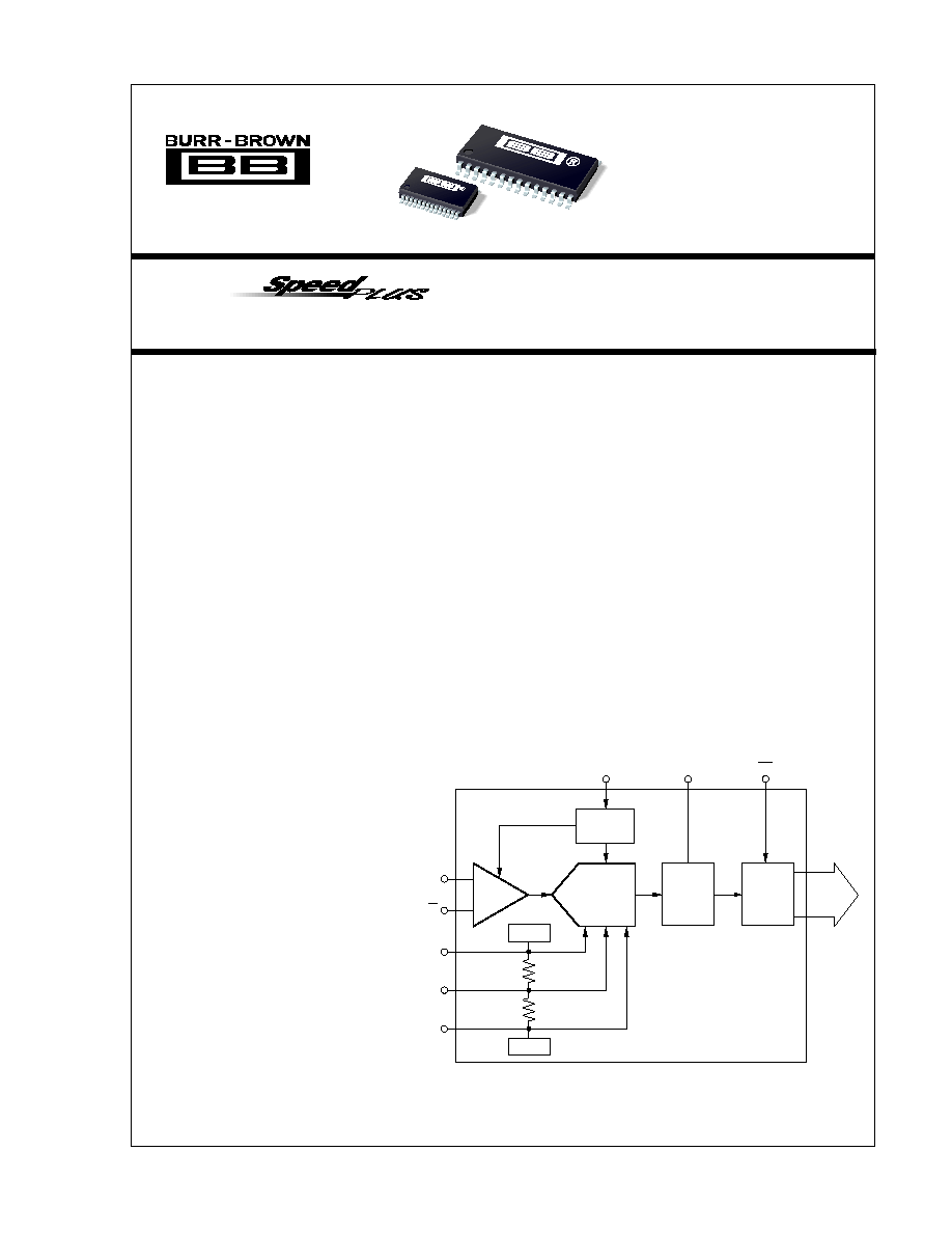
The ADS821 is a low power, monolithic 10-bit, 40MHz
analog-to-digital converter utilizing a small geometry
CMOS process. This COMPLETE converter includes
a 10-bit quantizer with internal track/hold, reference,
and a power down feature. It operates from a single
+5V power supply and can be configured to accept
either differential or single-ended input signals.
The ADS821 employs digital error correction to pro-
vide excellent Nyquist differential linearity perfor-
mance for demanding imaging applications. Its low
distortion, high SNR and high oversampling capability
give it the extra margin needed for telecommunications
and video applications.
This high performance converter is specified for AC
and DC performance at a 40MHz sampling rate. The
ADS821 is available in 28-pin SOIC and SSOP
packages.
Pipeline
A/D
Timing
Circuitry
Error
Correction
Logic
3-State
Outputs
T/H
10-Bit
Digital
Data
CLK
+1.25V
+3.25V
MSBI
OE
IN
IN
REFT
CM
REFB
10-Bit, 40MHz Sampling
ANALOG-TO-DIGITAL CONVERTER
©
1995 Burr-Brown Corporation
PDS-1291D
Printed in U.S.A. November, 1996
International Airport Industrial Park · Mailing Address: PO Box 11400, Tucson, AZ 85734 · Street Address: 6730 S. Tucson Blvd., Tucson, AZ 85706 · Tel: (520) 746-1111 · Twx: 910-952-1111
Internet: http://www.burr-brown.com/ · FAXLine: (800) 548-6133 (US/Canada Only) · Cable: BBRCORP · Telex: 066-6491 · FAX: (520) 889-1510 · Immediate Product Info: (800) 548-6132
APPLICATIONS
q
VIDEO DIGITIZING
q
ULTRASOUND IMAGING
q
GAMMA CAMERAS
q
SET-TOP BOXES
q
CABLE MODEMS
q
CCD IMAGING
Color Copiers
Scanners
Camcorders
Security Cameras
Fax Machines
q
IF AND BASEBAND DIGITIZATION
q
TEST INSTRUMENTATION
2
ADS821
®
The information provided herein is believed to be reliable; however, BURR-BROWN assumes no responsibility for inaccuracies or omissions. BURR-BROWN assumes
no responsibility for the use of this information, and all use of such information shall be entirely at the user's own risk. Prices and specifications are subject to change
without notice. No patent rights or licenses to any of the circuits described herein are implied or granted to any third party. BURR-BROWN does not authorize or warrant
any BURR-BROWN product for use in life support devices and/or systems.
ADS821U (SOIC)
ADS821E (SSOP)
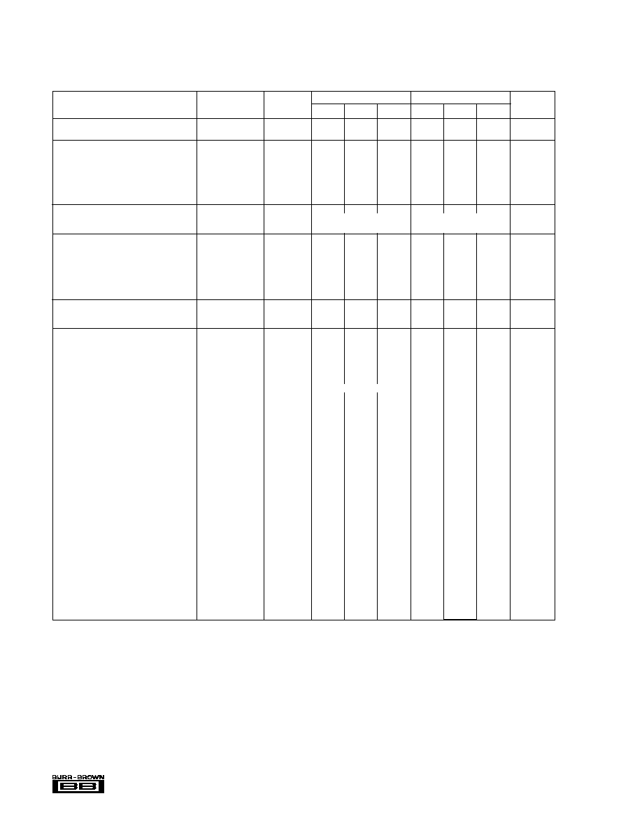
PARAMETER
CONDITIONS
TEMP
MIN
TYP
MAX
MIN
TYP
MAX
UNITS
SPECIFICATIONS
At T
A
= +25
°
C, V
S
= +5V, Sampling Rate = 40MHz, with a 50% duty cycle clock having a 2ns rise/fall time, unless otherwise noted.
TTL/HCT Compatible CMOS
Falling Edge
TTL/HCT Compatible CMOS
Falling Edge
Resolution
10
T
Bits
Specified Temperature Range
T
AMBIENT
40
+85
T
(1)
T
°
C
ANALOG INPUT
Differential Full Scale Input Range
+1.25
+3.25
T
T
V
Common-Mode Voltage
2.25
T
V
Analog Input Bandwidth (3dB)
Small Signal
20dBFS
(2)
Input
+25
°
C
120
T
MHz
Full Power
0dBFS Input
+25
°
C
65
T
MHz
Input Impedance
1.25 || 4
T
M
|| pF
DIGITAL INPUT
Logic Family
Convert Command
Start Conversion
ACCURACY
(3)
Gain Error
+25
°
C
±
0.6
±
1.5
T
T
%
Full
±
1.1
±
2.5
T
T
%
Gain Tempco
±
85
T
ppm/
°
C
Power Supply Rejection of Gain
Delta +V
S
=
±
5%
+25
°
C
0.01
0.15
T
T
%FSR/%
Input Offset Error
Full
±
2.1
±
3.5
T
T
%
Power Supply Rejection of Offset
Delta +V
S
=
±
5%
+25
°
C
0.02
0.15
T
T
%FSR/%
CONVERSION CHARACTERISTICS
Sample Rate
10k
40M
T
T
Sample/s
Data Latency
6.5
T
Convert Cycle
DYNAMIC CHARACTERISTICS
Differential Linearity Error
t
H
= 13ns
(4)
f = 500kHz
+25
°
C
±
0.5
±
1.0
T
T
LSB
0
°
C to +70
°
C
±
0.6
±
1.0
T
T
LSB
f = 12MHz
+25
°
C
±
0.5
±
1.0
T
T
LSB
0
°
C to +70
°
C
±
0.6
±
1.0
T
T
LSB
No Missing Codes
0
°
C to +70
°
C
Guaranteed
T
Integral Linearity Error at f = 500kHz
0
°
C to +70
°
C
±
0.5
±
2.0
T
T
LSB
Spurious-Free Dynamic Range (SFDR)
f = 500kHz (1dBFS input)
+25
°
C
60
70
T
T
dBFS
Full
54
67
T
T
dBFS
f = 12MHz (1dBFS input)
+25
°
C
58
63
T
T
dBFS
Full
54
62
T
T
dBFS
Two-Tone Intermodulation Distortion (IMD)
(5)
f = 4.4MHz and 4.5MHz (7dBFS each tone)
+25
°
C
61
T
dBc
Full
60
T
dBc
Signal-to-Noise Ratio (SNR)
f = 500kHz (1dBFS input)
+25
°
C
57
59
55
T
dB
Full
55
59
53
T
dB
f = 12MHz (1dBFS input)
+25
°
C
56
58
54
T
dB
Full
54
58
52
T
dB
Signal-to-(Noise + Distortion) (SINAD)
f = 500kHz (1dBFS input)
+25
°
C
56
58.5
T
T
dB
Full
52
58
T
T
dB
f = 12MHz (1dBFS input)
+25
°
C
53
57
T
T
dB
Full
50
56
T
T
dB
Differential Gain Error
NTSC or PAL
+25
°
C
0.5
T
%
Differential Phase Error
NTSC or PAL
+25
°
C
0.1
T
degrees
Effective Bits
(6)
f
IN
= 3.58MHz
+25
°
C
9.3
T
Bits
Aperture Delay Time
+25
°
C
2
T
ns
Aperture Jitter
+25
°
C
7
T
ps rms
Overvoltage Recovery Time
(7)
1.5x Full Scale Input
+25
°
C
2
T
ns
NOTE: (1) An asterisk (
T
) indicates same specifications as the ADS821U. (2) dBFS refers to dB below Full Scale. (3) Percentage accuracies are referred to
the internal A/D Full Scale Range of 4Vp-p. (4) Refer to Timing Diagram footnotes for the differential linearity performance conditions for the SOIC and SSOP
packages. (5) IMD is referred to the larger of the two input signals. If referred to the peak envelope signal (
0dB), the intermodulation products will be 7dB lower.
(6) Based on (SINAD 1.76)/6.02. (7) No "rollover" of bits.
3
®
ADS821
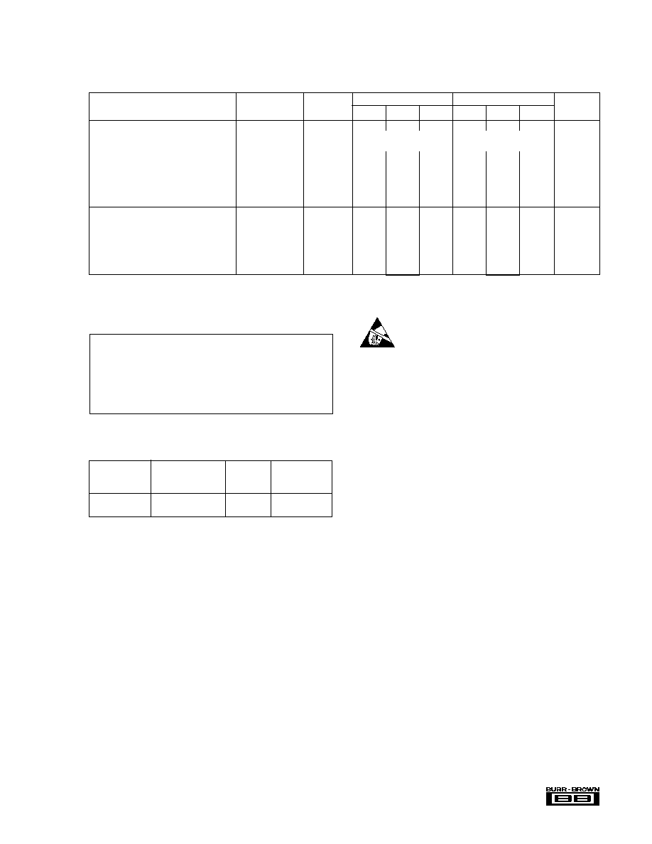
OUTPUTS
Logic Family
Logic Coding
Logic Selectable
Logic Levels
Logic "LO",
Full
0
0.4
T
T
V
C
L
= 15pF max
Logic "HI",
Full
+2.5
+V
S
T
T
V
C
L
= 15pF max
3-State Enable Time
20
40
T
T
ns
3-State Disable Time
Full
2
10
T
T
ns
POWER SUPPLY REQUIREMENTS
Supply Voltage: +V
S
Operating
Full
+4.75
+5
+5.25
T
T
T
V
Supply Current: +I
S
Operating
+25
°
C
76
88
T
T
T
mA
Operating
Full
78
90
T
T
T
mA
Power Consumption
Operating
+25
°
C
380
440
T
T
T
mW
Operating
Full
390
450
T
T
T
mW
Thermal Resistance,
JA
75
50
°
C/W
T
Specifications same as ADS821U.
ADS821U (SOIC)
ADS821E (SSOP)
PARAMETER
CONDITIONS
TEMP
MIN
TYP
MAX
MIN
TYP
MAX
UNITS
TTL/HCT Compatible CMOS
SOB or BTC
TTL/HCT Compatible CMOS
SOB or BTC
SPECIFICATIONS
(CONT)
At T
A
= +25
°
C, V
S
= +5V, Sampling Rate = 40MHz, with a 50% duty cycle clock having a 2ns rise/fall time, unless otherwise noted.
PACKAGE
DRAWING
TEMPERATURE
PRODUCT
PACKAGE
NUMBER
(1)
RANGE
ADS821U
28-Pin SOIC
217
40
°
C to +85
°
C
ADS821E
28-Pin SSOP
324
40
°
C to +85
°
C
NOTE: (1) For detailed drawing and dimension table, please see end of data
sheet, or Appendix C of Burr-Brown IC Data Book.
PACKAGE/ORDERING INFORMATION
ELECTROSTATIC
DISCHARGE SENSITIVITY
This integrated circuit can be damaged by ESD. Burr-Brown
recommends that all integrated circuits be handled with ap-
propriate precautions. Failure to observe proper handling and
installation procedures can cause damage.
Electrostatic discharge can cause damage ranging from
performance degradation to complete device failure. Burr-
Brown Corporation recommends that all integrated circuits be
handled and stored using appropriate ESD protection
methods.
ABSOLUTE MAXIMUM RATINGS
+V
S
....................................................................................................... +6V
Analog Input .............................................................. 0V to (+V
S
+ 300mV)
Logic Input ................................................................ 0V to (+V
S
+ 300mV)
Case Temperature ......................................................................... +100
°
C
Junction Temperature .................................................................... +150
°
C
Storage Temperature ..................................................................... +125
°
C
External Top Reference Voltage (REFT) .................................. +3.4V max
External Bottom Reference Voltage (REFB) .............................. +1.1V min
NOTE: Stresses above these ratings may permanently damage the device.
4
ADS821
®
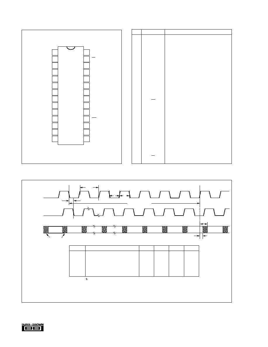
PIN
DESIGNATOR
DESCRIPTION
1
GND
Ground
2
B1
Bit 1, Most Significant Bit
3
B2
Bit 2
4
B3
Bit 3
5
B4
Bit 4
6
B5
Bit 5
7
B6
Bit 6
8
B7
Bit 7
9
B8
Bit 8
10
B9
Bit 9
11
B10
Bit 10, Least Significant Bit
12
DNC
Do not connect.
13
DNC
Do not connect.
14
GND
Ground
15
+V
S
+5V Power Supply
16
CLK
Convert Clock Input, 50% Duty Cycle
17
+V
S
+5V Power Supply
18
OE
HI: High Impedance State. LO or Floating: Nor-
mal Operation. Internal pull-down resistor.
19
MSBI
Most Significant Bit Inversion, HI: MSB inverted
for complementary output. LO or Floating: Straight
output. Internal pull-down resistor.
20
+V
S
+5V Power Supply
21
REFB
Bottom Reference Bypass. For external bypass-
ing of internal +1.25V reference.
22
CM
Common-Mode Voltage. It is derived by (REFT +
REFB)/2.
23
REFT
Top Reference Bypass. For external bypassing
of internal +3.25V reference.
24
+V
S
+5V Power Supply
25
GND
Ground
26
IN
Input
27
IN
Complementary Input
28
GND
Ground
PIN DESCRIPTIONS
PIN CONFIGURATION
TOP VIEW
SOIC
GND
Bit 1(MSB)
Bit 2
Bit 3
Bit 4
Bit 5
Bit 6
Bit 7
Bit 8
Bit 9
Bit 10 (LSB)
DNC
DNC
GND
GND
IN
IN
GND
+V
S
REFT
CM
REFB
+V
S
MSBI
OE
+V
S
CLK
+V
S
1
2
3
4
5
6
7
8
9
10
11
12
13
14
28
27
26
25
24
23
22
21
20
19
18
17
16
15
ADS821
DNC: Do Not Connect
TIMING DIAGRAM
SYMBOL
DESCRIPTION
MIN
TYP
MAX
UNITS
t
CONV
Convert Clock Period
25
100
µ
s
ns
t
L
Clock Pulse Low
12
12.5
ns
t
H
Clock Pulse High
12
(2)
12.5
ns
t
D
Aperture Delay
2
ns
t
1
Data Hold Time, C
L
= 0pF
3.9
ns
t
2
New Data Delay Time, C
L
= 15pF max
12.5
ns
NOTE: (1) " " indicates the portion of the waveform that will stretch out at slower sample rates.
(2) t
H
must be 13ns minimum if no missing codes is desired only for the conditions of t
CONV
28ns
and f
IN
<2MHz for the SOIC package. For best performance in the SSOP package, t
H
must be 13ns
minimum for all input frequencies and t
CONV
28ns. Refer to the Clock Requirements for a possible
clock skew circuit for this condition.
Track
Hold
"N"
Hold
"N + 1"
Hold
"N + 2"
Hold
"N + 3"
Hold
"N + 4"
Hold
"N + 5"
Hold
"N + 6"
Track
Data Valid
N-7
Data Valid
N-6
INTERNAL
TRACK/HOLD
CONVERT
CLOCK
OUTPUT
DATA
t
D
t
2
t
1
DATA LATENCY
(6.5 Clock Cycles)
t
CONV
t
L
t
H
Track
Track
Track
Track
N-3
N-5
N-4
N-2
N-1
N
Track
Track
Data Valid
N-8
(1)
Data Invalid
5
®
ADS821
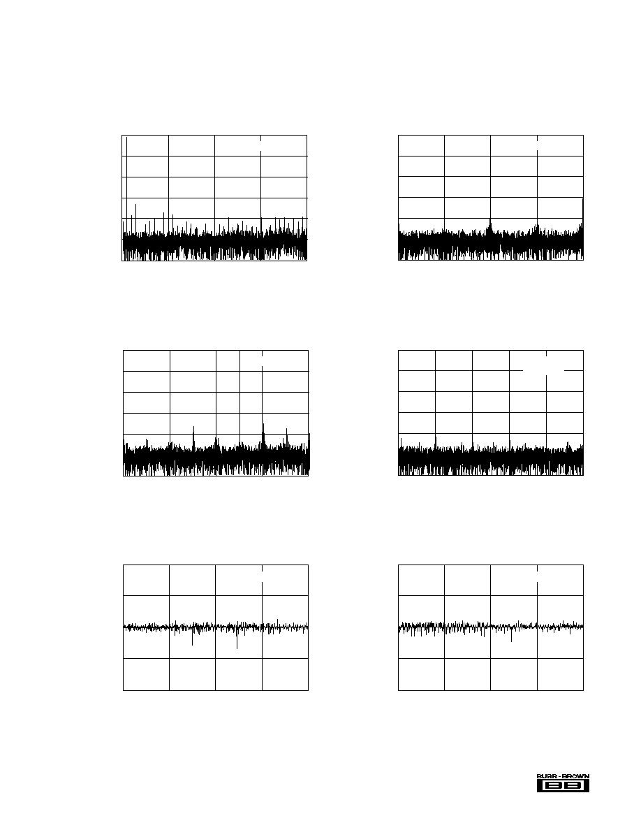
SPECTRAL PERFORMANCE
Frequency (MHz)
Amplitude (dB)
0
5
10
15
20
0
20
40
60
80
100
120
f
IN
= 12MHz
TYPICAL PERFORMANCE CURVES
At T
A
= +25
°
C, V
S
= +5V, Sampling Rate = 40MHz, with a 50% duty cycle clock having a 2ns rise/fall time, unless otherwise noted.
SPECTRAL PERFORMANCE
Frequency (MHz)
Amplitude (dB)
0
5
10
15
20
0
20
40
60
80
100
120
f
IN
= 500kHz
SPECTRAL PERFORMANCE
Frequency (MHz)
Amplitude (dB)
0
5
10
15
20
0
20
40
60
80
100
120
f
IN
= 5MHz
SPECTRAL PERFORMANCE
Frequency (MHz)
Amplitude (dB)
0
1.0
2.0
3.0
4.0
5.0
0
20
40
60
80
100
120
f
IN
= 1MHz
f
S
= 10MHz
DIFFERENTIAL LINEARITY ERROR
Code
DLE (LSB)
2.0
1.0
0
1.0
2.0
Code
0
256
512
768
1024
f
IN
= 500kHz
DIFFERENTIAL LINEARITY ERROR
Code
DLE (LSB)
2.0
1.0
0
1.0
2.0
Code
0
256
512
768
1024
f
IN
= 12MHz
6
ADS821
®
TYPICAL PERFORMANCE CURVES
(CONT)
At T
A
= +25
°
C, V
S
= +5V, Sampling Rate = 40MHz, with a 50% duty cycle clock having a 2ns rise/fall time, unless otherwise noted.
0
20
40
60
80
100
120
TWO-TONE INTERMODULATION
Amplitude (dB)
0.0
5.00
10.00
15.00
20.00
Frequency (MHz)
f
1
= 4.47MHz
f
2
= 4.39MHz
DYNAMIC PERFORMANCE vs INPUT FREQUENCY
Frequency (MHz)
SFDR, SNR (dB)
70
65
60
55
0.1
1
10
100
SFDR
SNR
100
80
60
40
20
0
Input Amplitude (dBm)
SFDR (dBFS)
SWEPT POWER SFDR
50
40
30
20
10
0
10
f
IN
= 12MHz
60
50
40
30
20
10
0
Input Amplitude (dBm)
SWEPT POWER SNR
50
40
30
20
10
0
10
SNR (dB)
f
IN
= 12MHz
4.0
2.0
0
2.0
4.0
INTEGRAL LINEARITY ERROR
Code
ILE (LSB)
f
IN
= 500kHz
0.0
0.20
0.40
0.60
0.80
1.0
65
60
55
50
45
40
DYNAMIC PERFORMANCE
vs SINGLE-ENDED FULL-SCALE INPUT RANGE
Dynamic Range (dB)
2
3
4
Single-Ended Full-Scale Input Range (Vp-p)
SNR (f
IN
= 12MHz)
SFDR (f
IN
= 500kHz)
SNR (f
IN
= 500kHz)
SFDR (f
IN
= 12MHz)
NOTE: REFT
EXT
varied, REFB is fixed at the internal value of +1.25V.
7
®
ADS821
TYPICAL PERFORMANCE CURVES
(CONT)
At T
A
= +25
°
C, V
S
= +5V, Sampling Rate = 40MHz, with a 50% duty cycle clock having a 2ns rise/fall time, unless otherwise noted.
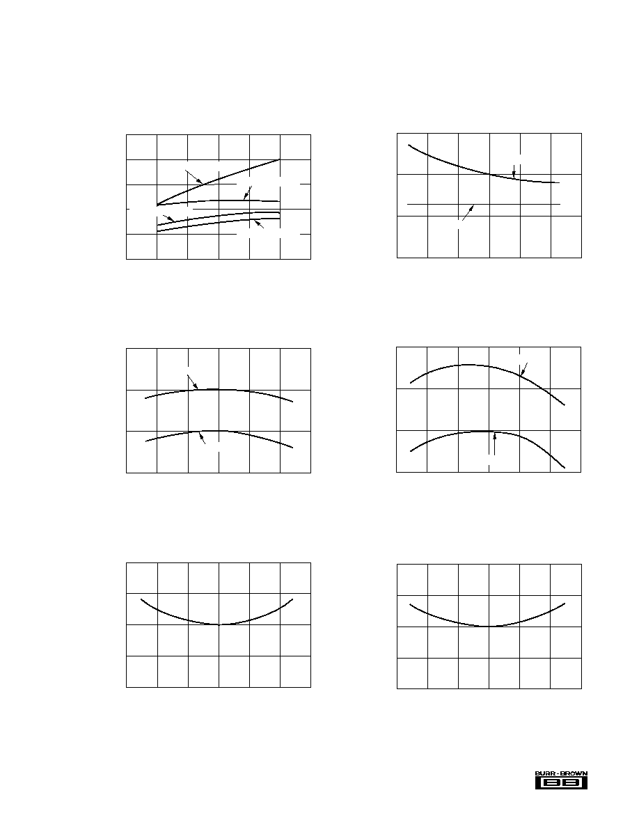
SPURIOUS FREE DYNAMIC RANGE
vs TEMPERATURE
Ambient Temperature (°C)
SFDR (dBFS)
80
70
60
50
50
25
0
25
50
75
100
f
IN
= 500kHz
f
IN
= 12MHz
POWER DISSIPATION vs TEMPERATURE
Ambient Temperature (°C)
Power (mW)
335
330
325
50
25
0
25
50
75
100
SIGNAL-TO-NOISE RATIO vs TEMPERATURE
Ambient Temperature (°C)
SNR (dB)
60
59
58
57
50
25
0
25
50
75
100
f
IN
= 500kHz
f
IN
= 12MHz
SIGNAL-TO-(NOISE + DISTORTION)
vs TEMPERATURE
Ambient Temperature (°C)
SINAD (dB)
59
58
57
56
50
25
0
25
50
75
100
f
IN
= 500kHz
f
IN
= 10MHz
SUPPLY CURRENT vs TEMPERATURE
Ambient Temperature (°C)
I
Q
(mA)
67
66
65
50
25
0
25
50
75
100
75
70
65
60
55
70
DYNAMIC PERFORMANCE
vs DIFFERENTIAL FULL-SCALE INPUT RANGE
Dynamic Range (dB)
2
3
4
Differential Full-Scale Input Range (Vp-p)
NOTE: REFT
EXT
varied, REFB is fixed at internal value of +1.25V.
SNR (f
IN
= 500kHz)
SNR (f
IN
= 12MHz)
SFDR (f
IN
= 12MHz)
SFDR (f
IN
= 500kHz)
8
ADS821
®
TYPICAL PERFORMANCE CURVES
(CONT)
At T
A
= +25
°
C, V
S
= +5V, Sampling Rate = 40MHz, with a 50% duty cycle clock having a 2ns rise/fall time, unless otherwise noted.
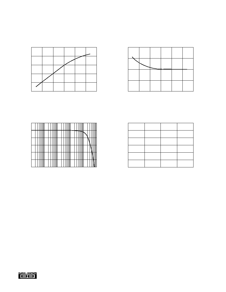
GAIN ERROR vs TEMPERATURE
Ambient Temperature (°C)
Gain (% FSR)
0
0.25
0.5
0.75
1.0
1.25
50
25
0
25
50
75
100
OFFSET ERROR vs TEMPERATURE
Ambient Temperature (°C)
Offset (% FSR)
1.75
2.0
2.25
50
25
0
25
50
75
100
TRACK-MODE SMALL-SIGNAL INPUT BANDWIDTH
Frequency (Hz)
Track-Mode Input Response (dB)
10k
1
0
1
2
3
4
5
100k
1M
10M
100M
1G
OUTPUT NOISE HISTOGRAM (NO SIGNAL)
Counts
1.2M
1M
0.8M
0.6M
0.4M
0.2M
0.0
Code
N2
N1
N
N+1
N+2
9
®
ADS821
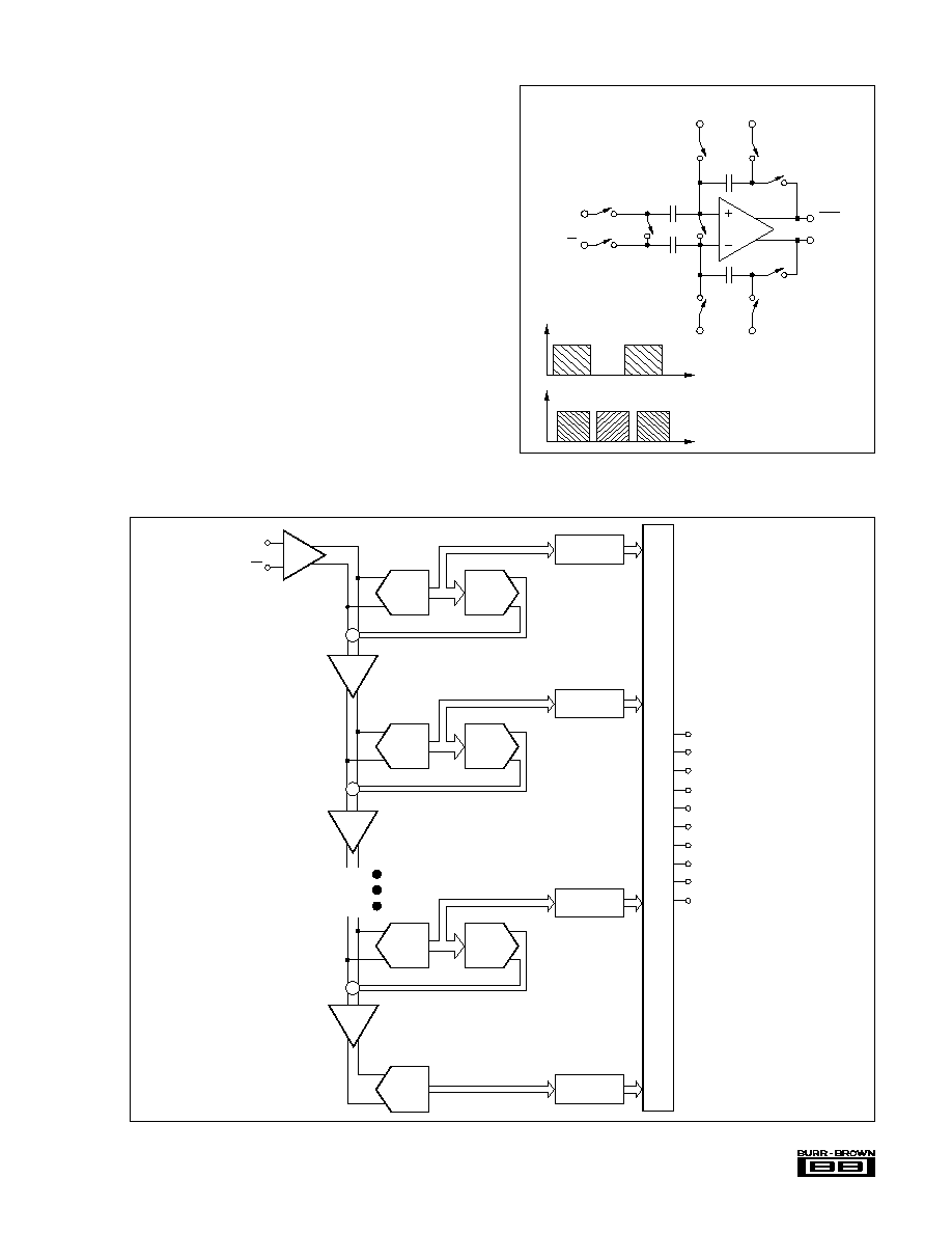
FIGURE 1. Input Track/Hold Configuration with Timing
Signals.
FIGURE 2. Pipeline A/D Architecture.
1
1
2
1
1
1
1
1
2
1
2
1
2
IN
IN
OUT
OUT
Op Amp
Bias
V
CM
Op Amp
Bias
V
CM
C
H
C
I
C
I
C
H
Input Clock (50%)
Internal Non-overlapping Clock
B1 (MSB)
B2
B3
B4
B5
B6
B7
B8
B9
B10 (LSB)
2-Bit
DAC
2-Bit
Flash
Input
T/H
Digital Delay
x2
x2
2-Bit
DAC
2-Bit
Flash
Digital Delay
2-Bit
Flash
Digital Delay
2-Bit
DAC
2-Bit
Flash
Digital Delay
x2
Digital Error Correction
IN
IN
STAGE 1
STAGE 2
STAGE 8
STAGE 9
+
+
+
THEORY OF OPERATION
The ADS821 is a high speed sampling analog-to-digital
converter with pipelining. It uses a fully differential archi-
tecture and digital error correction to guarantee 10-bit reso-
lution. The differential track/hold circuit is shown in Figure
1. The switches are controlled by an internal clock which has
a non-overlapping two phase signal,
1 and
2. At the
sampling time the input signal is sampled on the bottom
plates of the input capacitors. In the next clock phase,
2, the
bottom plates of the input capacitors are connected together
and the feedback capacitors are switched to the op amp
output. At this time the charge redistributes between C
I
and
C
H
, completing one track/hold cycle. The differential output
is a held DC representation of the analog input at the sample
time. The track/hold circuit can also convert a single-ended
input signal into a fully differential signal for the quantizer.
The pipelined quantizer architecture has 9 stages with each
stage containing a two-bit quantizer and a two bit digital-to-
analog converter, as shown in Figure 2. Each two-bit quan-
tizer stage converts on the edge of the sub-clock, which is
twice the frequency of the externally applied clock. The
output of each quantizer is fed into its own delay line to
10
ADS821
®
time-align it with the data created from the following quan-
tizer stages. This aligned data is fed into a digital error
correction circuit which can adjust the output data based on
the information found on the redundant bits. This technique
gives the ADS821 excellent differential linearity and guar-
antees no missing codes at the 10-bit level.
The output data is available in Straight Offset Binary (SOB)
or Binary Two's Complement (BTC) format.
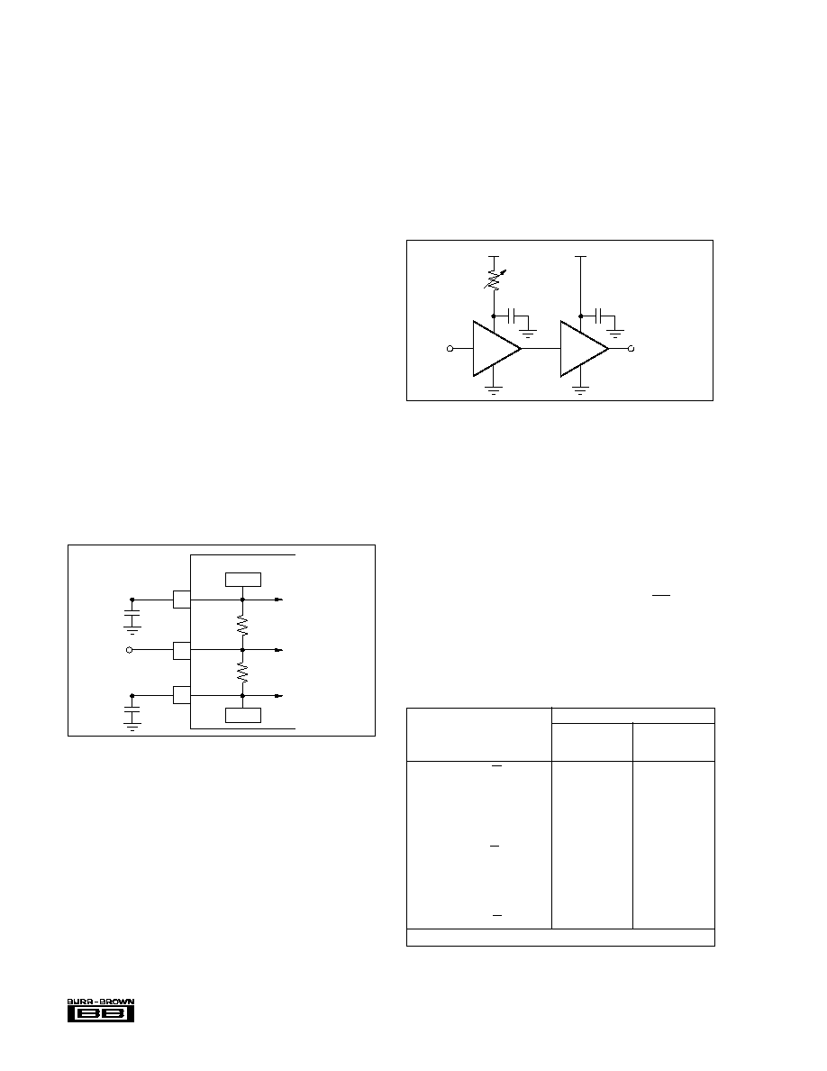
THE ANALOG INPUT AND INTERNAL REFERENCE
The analog input of the ADS821 can be configured in
various ways and driven with different circuits, depending
on the nature of the signal and the level of performance
desired. The ADS821 has an internal reference that sets the
full scale input range of the A/D. The differential input range
has each input centered around the common-mode of +2.25V,
with each of the two inputs having a full scale range of
+1.25V to +3.25V. Since each input is 2V peak-to-peak and
180
°
out of phase with the other, a 4V differential input
signal to the quantizer results. As shown in Figure 3, the
positive full scale reference (REFT) and the negative full
scale reference (REFB) are brought out for external bypass-
ing. In addition, the common-mode voltage (CM) may be
used as a reference to provide the appropriate offset for the
driving circuitry. However, care must be taken not to appre-
ciably load this reference node. For more information re-
garding external references, single-ended inputs, and
ADS821 drive circuits, refer to the applications section.
·
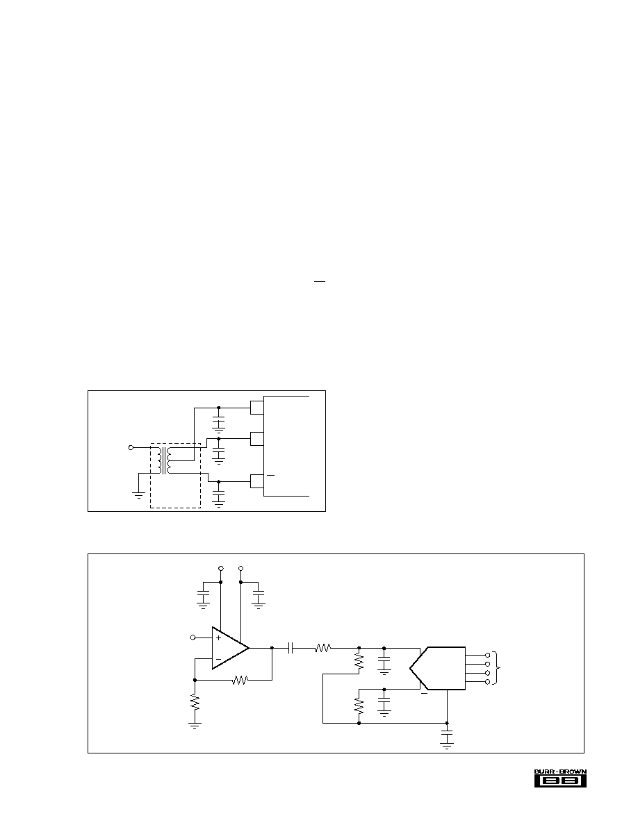
For most applications, the clock duty should be set to
50%. However, for applications requiring no missing
codes, a slight skew in the duty cycle will improve DNL
performance for conversion rates >35MHz and input
frequencies <2MHz (see Timing Diagram) in the SOIC
package. For the best performance in the SSOP package,
the clock should be skewed under all input frequencies
with conversion rates >35MHz. A possible method for
skewing the 50% duty cycle source is shown in Figure 4.
FIGURE 3. Internal Reference Structure.
+1.25V
+3.25V
2k
2k
0.1µF
0.1µF
+2.25V
REFT
REFB
CM
ADS821
To
Internal
Comparators
21
22
23
CLOCK REQUIREMENTS
The CLK pin accepts a CMOS level clock input. Both the
rising and falling edges of the externally applied clock
control the various interstage conversions in the pipeline.
Therefore, the clock signal's jitter, rise/fall times and duty
cycle can affect conversion performance.
· Low clock jitter is critical to SNR performance in fre-
quency-domain signal environments.
· Clock rise and fall times should be as short as possible
(<2ns for best performance).
FIGURE 4. Clock Skew Circuit.
0.1µF
R
V
2k
V
DD
0.1µF
V
DD
CLK
OUT
CLK
IN
IC2
IC1
IC1, IC2 = ACT04
R
V
= 217
, typical
DIGITAL OUTPUT DATA
The 10-bit output data is provided at CMOS logic levels.
There is a 6.5 clock cycle data latency from the start convert
signal to the valid output data. The standard output coding
is Straight Offset Binary where a full scale input signal
corresponds to all "1's" at the output. This condition is met
with pin 19 "LO" or Floating due to an internal pull-down
resistor. By applying a high voltage to this pin, a Binary
Two's Complement output will be provided where the most
significant bit is inverted. The digital outputs of the ADS821
can be set to a high impedance state by driving OE (pin 18)
with a logic "HI". Normal operation is achieved with pin 18
"LO" or Floating due to internal pull-down resistors. This
function is provided for testability purposes and is not meant
to drive digital buses directly or be dynamically changed
during the conversion process.
OUTPUT CODE
SOB
BTC
PIN 19
PIN 19
DIFFERENTIAL INPUT
(1)
FLOATING or LO
HI
+FS (IN = +3.25V, IN = +1.25V)
1111111111
0111111111
+FS 1LSB
1111111111
0111111111
+FS 2LSB
1111111110
0111111110
+3/4 Full Scale
1110000000
0110000000
+1/2 Full Scale
1100000000
0100000000
+1/4 Full Scale
1010000000
0010000000
+1LSB
1000000001
0000000001
Bipolar Zero (IN = IN = +2.25V)
1000000000
0000000000
1LSB
0111111111
1111111111
1/4 Full Scale
0110000000
1110000000
1/2 Full Scale
0100000000
1100000000
3/4 Full Scale
0010000000
1010000000
FS +1LSB
0000000001
1000000001
FS (IN = +1.25V, IN = +3.25V)
0000000000
1000000000
Note: In the single-ended input mode, +FS = +4.25V and FS = +0.25V.
TABLE I. Coding Table for the ADS821.
11
®
ADS821
APPLICATIONS
DRIVING THE ADS821
The ADS821 has a differential input with a common-mode
of +2.25V. For AC-coupled applications, the simplest way
to create this differential input is to drive the primary
winding of a transformer with a single-ended input. A
differential output is created on the secondary if the center
tap is tied to the common-mode voltage (CM) of +2.25V per
Figure 5. This transformer-coupled input arrangement pro-
vides good high frequency AC performance. It is important
to select a transformer that gives low distortion and does not
exhibit core saturation at full scale voltage levels. Since the
transformer does not appreciably load the ladder, there is no
need to buffer the common-mode (CM) output in this in-
stance. In general, it is advisable to keep the current draw
from the CM output pin below 0.5
µ
A to avoid nonlinearity
in the internal reference ladder. A FET input operational
amplifier such as the OPA130 can provide a buffered refer-
ence for driving external circuitry. The analog IN and IN
inputs should be bypassed with 22pF capacitors to minimize
track/hold glitches and to improve high input frequency
performance.
Figure 6 shows an AC-coupled single-ended input interface
circuit using the low cost, current feedback OPA658 as the
active gain stage. When testing this configuration in gains of
+4, +5.8 and +8.2, it was noted that reducing the feedback
resistor of the OPA658 from the typical 402
to 360
resulted in a wider bandwidth, thus improving distortion at
higher gains. The gain resistor was scaled to 120
, 75
and
50
for each of the three gain settings. The two 330
resistors set the RC time constant and the values can be
varied, although higher values will have the effect of moving
the corner frequency of the created high-pass filter down. In
Figure 6, the 3dB point is set at 4.2kHz.
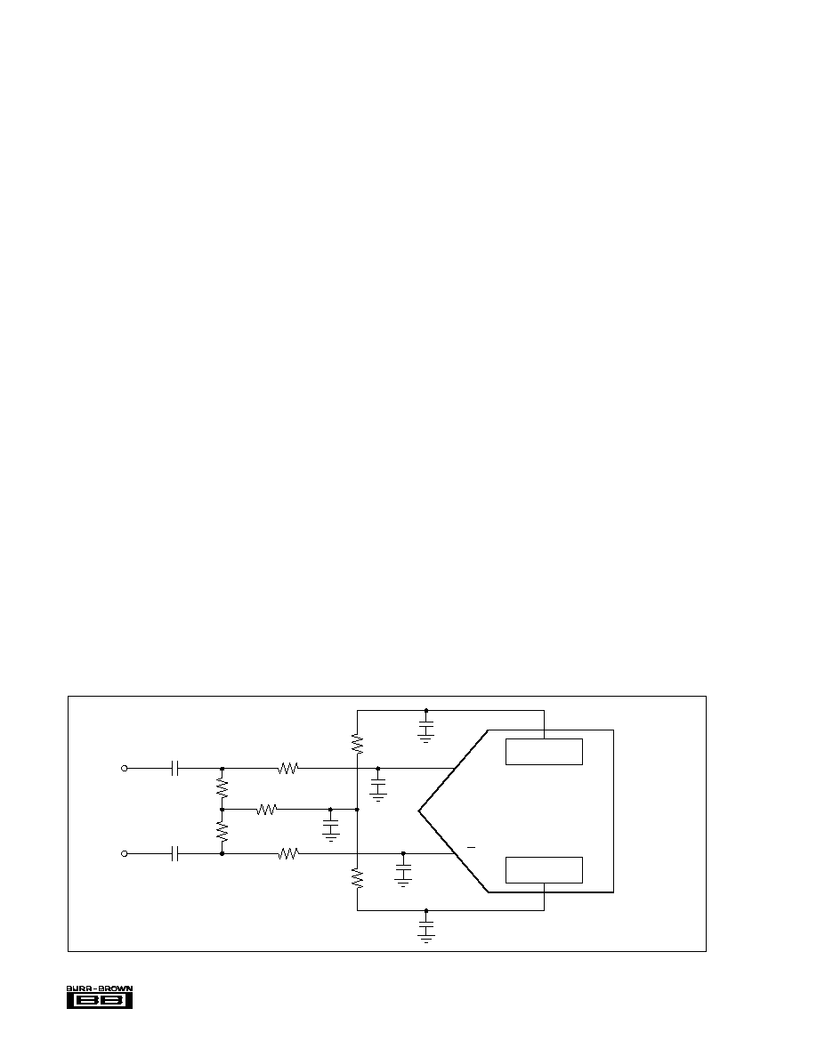
Figure 7 illustrates another possible low cost interface circuit
which utilizes resistors and capacitors in place of a trans-
former. Depending on the signal bandwidth, the component
values should be carefully selected in order to maintain the
performance outlined in the data sheet. The input capacitors,
C
IN
, and the input resistors, R
IN
, create a high-pass filter with
the lower corner frequency at f
C
= 1/(2
R
IN
C
IN
). The corner
frequency can be reduced by either increasing the value of
R
IN
or C
IN
. If the circuit operates with a 50
or 75
impedance level, the resistors are fixed and only the value of
the capacitor can be increased. Usually AC-coupling capaci-
tors are electrolytic or tantalum capacitors with values of
1
µ
F or higher. It should be noted that these large capacitors
become inductive with increased input frequency, which
could lead to signal amplitude errors or oscillation. To
maintain a low AC-coupling impedance throughout the sig-
nal band, a small value (e.g. 1
µ
F) ceramic capacitor could be
added in parallel with the polarized capacitor.
Capacitors C
SH1
and C
SH2
are used to minimize current
glitches resulting from the switching in the input track and
hold stage and to improve signal-to-noise performance. These
capacitors can also be used to establish a low-pass filter and
effectively reduce the noise bandwidth. In order to create a
real pole, resistors R
SER1
and R
SER2
were added in series with
each input. The cut-off frequency of the filter is determined
by f
C
= 1/(2
R
SER
·(C
SH
+C
ADC
)) where R
SER
is the resistor in
series with the input, C
SH
is the external capacitor from the
input to ground, and C
ADC
is the internal input capacitance of
the A/D converter (typically 4pF).
Resistors R
1
and R
2
are used to derive the necessary common
mode voltage from the buffered top and bottom references.
FIGURE 5. AC-Coupled Single-Ended to Differential Drive
Circuit Using a Transformer.
FIGURE 6. Low-Cost AC-Coupled Single-Ended Input Circuit.
Mini-Circuits
T T1-6-KK81
or equivalent
22
26
27
CM
IN
IN
ADS821
AC Input
Signal
22pF
22pF
0.1
µ
F
ADS821
A
1
V
IN
R
G
OPA658
0.1 || 2.2
0.1 || 2.2
+5V
5V
I/O
360
330
330
IN
27
26
22
CM
+2.25V
IN
22pF
49.9
0.1
µ
F
0.1
µ
F
0.1
µ
F
12
ADS821
®
The total load of the resistor string should be selected so that
the current does not exceed 1mA. Although the circuit in
Figure 7 uses two resistors of equal value so that the common
mode voltage is centered between the top and bottom refer-
ence (+2.25V), it is not necessary to do so. In all cases the
center point, V
CM
, should be bypassed to ground in order to
provide a low impedance AC ground.
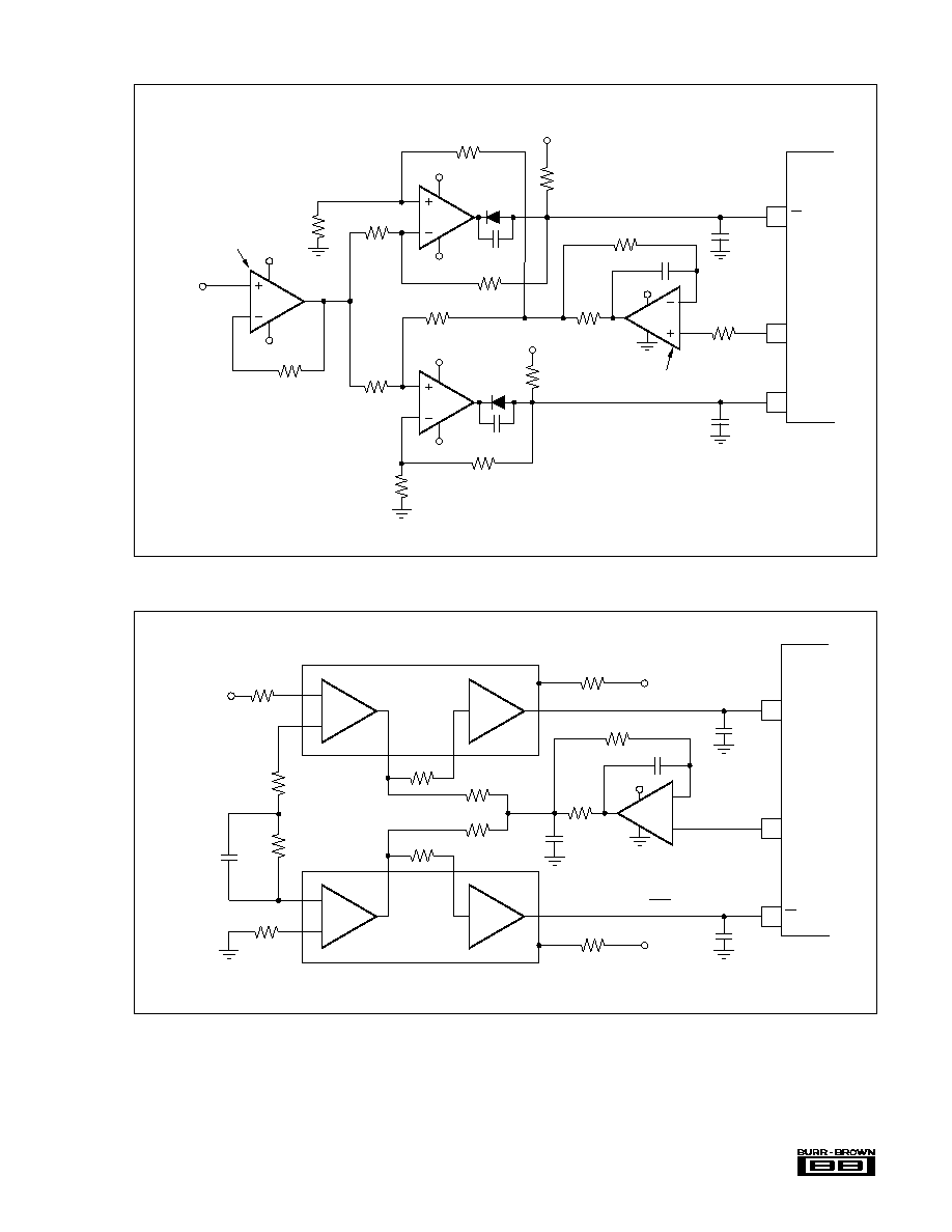
If the signal needs to be DC coupled to the input of the
ADS821, an operational amplifier input circuit is required.
In the differential input mode, any single-ended signal must
be modified to create a differential signal. This can be
accomplished by using two operational amplifiers, one in
the noninverting mode for the input and the other amplifier
in the inverting mode for the complementary input. The low
distortion circuit in Figure 8 will provide the necessary input
shifting required for signals centered around ground. It also
employs a diode for output level shifting to guarantee a low
distortion +3.25V output swing. Another DC-coupled circuit
is shown in Figure 9. Other amplifiers can be used in place
of the OPA642s if the lowest distortion is not necessary. If
output level shifting circuits are not used, care must be taken
to select operational amplifiers that give the necessary per-
formance when swinging to +3.25V with a
±
5V supply
operational amplifier. The OPA620 and OPA621, or the
lower power OPA650 or OPA651 can be used in place of the
OPA642s in Figure 8. In that configuration, the OPA650 and
OPA651 will typically swing to within 100mV of positive
full scale. If the OPA621 or OPA651 is used, the input
buffer must be configured in a gain of 2.
The ADS821 can also be configured with a single-ended
input full scale range of +0.25V to +4.25V by tying the
complementary input to the common-mode reference voltage
as shown in Figure 10. This configuration will result in
increased even-order harmonics, especially at higher input
frequencies. However, this tradeoff may be quite acceptable
for time-domain applications. The driving amplifier must
give adequate performance with a +0.25V to +4.25V output
swing in this case.
EXTERNAL REFERENCES AND ADJUSTMENT OF
FULL SCALE RANGE
The internal reference buffers are limited to approximately
1mA of output current. As a result, these internal +1.25V
and +3.25V references may be overridden by external refer-
ences that have at least 18mA (at room temperature) of
output drive capability. In this instance, the common-mode
voltage will be set halfway between the two references. This
feature can be used to adjust the gain error, improve gain
drift, or to change the full scale input range of the ADS821.
Changing the full scale range to a lower value has the benefit
of easing the swing requirements of external input amplifi-
ers. The external references can vary as long as the value of
the external top reference (REFT
EXT
) is less than or equal to
+3.4V and the value of the external bottom reference
(REFB
EXT
) is greater than or equal to +1.1V and the differ-
ence between the external references are greater than or
equal to 800mV.
For the differential configuration, the full scale input range
will be set to the external reference values that are selected.
For the single-ended mode, the input range is 2·(REFT
EXT
REFB
EXT
), with the common-mode being centered at
(REFT
EXT
+ REFB
EXT
)/2. Refer to the typical performance
curves for expected performance vs full scale input range.
The circuit in Figure 11 works completely on a single +5V
supply. As a reference element, it uses the micro-power
reference REF1004-2.5, which is set to a quiescent current
of 0.1mA. Amplifier A
2
is configured as a follower to buffer
the +1.25V generated from the resistor divider. To provide
the necessary current drive, a pull-down resistor, R
P
is
added.
Amplifier A
1
is configured as an adjustable gain stage, with
a range of approximately 1 to 1.32. The pull-up resistor
again relieves the op amp from providing the full current
drive. The value of the pull-up/down resistors is not critical
and can be varied to optimize power consumption. The need
for pull-up/down resistors depends only on the drive capa-
bility of the selected drive amplifier and thus can be omitted.
FIGURE 7. AC-Coupled Differential Input Circuit.
ADS8xx
*R
SER1
49.9
R
3
1k
R
2
(6k
)
R
1
(6k
)
C
2
0.1
µ
F
C
SH1
22pF
C
SH2
22pF
C
3
0.1
µ
F
C
1
0.1
µ
F
C
IN
0.1
µ
F
V
CM
C
IN
0.1
µ
F
R
IN1
25
R
IN2
25
*R
SER2
49.9
+3.25V
Top Reference
+1.25V
Bottom Reference
IN
NOTE: * indicates optional component.
IN
13
®
ADS821
50
1k
OTA
OPA660
OPA660
+1
+1
OPA130
1nF
OTA
5V
+5V
DC-Coupled
Input Signal
27 IN
22 CM
26 IN
ADS821
NOTE: Power supplies and bypassing not shown. The measured SNR performance with 12.5MHz input signal is 57dB with this driver circuit.
1k
500
500
1k
200
243
200
3
B
2
3
2
8
5
C
6
1
6
1
8
5
C
E
E
3
2
B
200
C
1
15pF
22pF
22pF
0.1µF
2k
V
OUT
V
OUT
5V
243
604
301
301
301
604
49.9
301
604
2.49k
2.49k
+2.25V
OPA642
OPA130
301
0.1µF
OPA642
OPA642
+5V
5V
+5V
(2)
+5V
5V
+5V
+5V
+5V
5V
BAS16
(1)
BAS16
(1)
301
24.9
Input Level
Shift Buffer
Optional
High Impedance
Input Amplifier
DC-Coupled
Input Signal
26 IN
22 CM
27 IN
ADS821
NOTES: (1) A Philips BAS16 diode or equivalent may be used.
(2) Supply bypassing not shown. (3) OPA620 or OPA650 may be
substituted. See "Driving the ADS820" section.
22pF
22pF
604
0.1µF
0.1µF
(3)
(3)
(3)
FIGURE 9. A Wideband DC-Coupled, Single-Ended to Differential Input Driver Circuit.
FIGURE 8. A Low Distortion DC-Coupled, Single-Ended to Differential Input Driver Circuit.
14
ADS821
®
results. Highly accurate phase-locked signal sources allow
high resolution FFT measurements to be made without using
data windowing functions. A low jitter signal generator such
as the HP8644A for the test signal, phase-locked with a low
jitter HP8022A pulse generator for the A/D clock, gives
excellent results. Low pass filtering (or bandpass filtering)
of test signals is absolutely necessary to test the low distor-
tion of the ADS821. Using a signal amplitude slightly lower
than full scale will allow a small amount of "headroom" so
that noise or DC offset voltage will not overrange the A/D
and cause clipping on signal peaks.
DYNAMIC PERFORMANCE DEFINITIONS
1. Signal-to-Noise-and-Distortion Ratio (SINAD):
10 log
2. Signal-to-Noise Ratio (SNR):
10 log
3. Intermodulation Distortion (IMD):
10 log
IMD is referenced to the larger of the test signals f
1
or f
2
.
Five "bins" either side of peak are used for calculation of
fundamental and harmonic power. The "0" frequency bin
(DC) is not included in these calculations as it is of little
importance in dynamic signal processing applications.
FIGURE 10. Single-Ended Input Connection.
22
26
27
CM
IN
IN
ADS821
0.1µF
Single-Ended
Input Signal
Full Scale = +0.25V to +4.25V with internal references.
22pF
PC BOARD LAYOUT AND BYPASSING
A well-designed, clean PC board layout will assure proper
operation and clean spectral response. Proper grounding and
bypassing, short lead lengths, and the use of ground planes
are particularly important for high frequency circuits. Mul-
tilayer PC boards are recommended for best performance
but if carefully designed, a two-sided PC board with large,
heavy ground planes can give excellent results. It is recom-
mended that the analog and digital ground pins of the
ADS821 be connected directly to the analog ground plane.
In our experience, this gives the most consistent results. The
A/D power supply commons should be tied together at the
analog ground plane. Power supplies should be bypassed
with 0.1
µ
F ceramic capacitors as close to the pin as possible.
DYNAMIC PERFORMANCE TESTING
The ADS821 is a high performance converter and careful
attention to test techniques is necessary to achieve accurate
Sinewave Signal Power
Noise + Harmonic Power (first 15 harmonics)
Highest IMD Product Power (to 5th-order)
Sinewave Signal Power
Sinewave Signal Power
Noise Power
FIGURE 11. Optional External Reference to Set the Full-Scale Range Utilizing a Dual, Single-Supply Op Amp.
2k
+2.5V to +3.25V
+5V
+5V
R
P
220
R
P
220
10k
6.2k
0.1
µ
F
+2.5V
10k
1/2
OPA2234
1/2
OPA2234
A
1
A
2
Bottom
Reference
Top
Reference
REF1004
+1.25V
10k
10k
*
10k
*
NOTE: (*) Use parts alternatively for adjustment capability.
15
®
ADS821
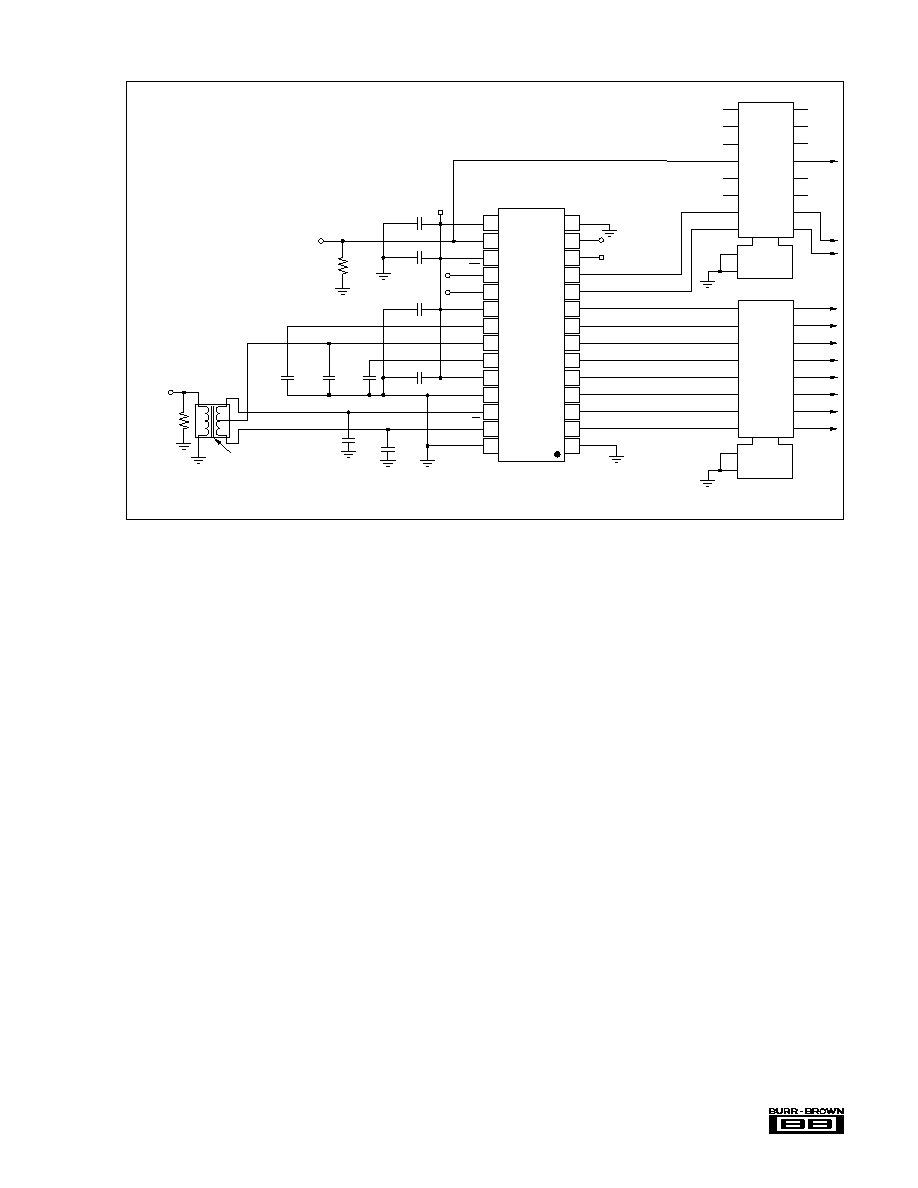
FIGURE 12. ADS821 Interface Schematic with AC-Coupling and External Buffers.
GND
DNC
DNC
LSB
MSB
GND
11
12
13
14
15
16
17
18
9
8
7
6
5
4
3
2
1
19
+V
S
CLK
+V
S
OE
MSBI
+V
S
REFB
CM
REFT
+V
S
GND
IN
IN
GND
15
16
17
18
19
20
21
22
23
24
25
26
27
28
14
13
12
11
10
9
8
7
6
5
4
3
2
1
ADS821
0.1µF
0.1µF
0.1µF
0.1µF
0.1µF
0.1µF
0.1µF
R
1
50
R
2
50
Ext
Clk
AC Input
Signal
11
12
13
14
15
16
17
18
9
8
7
6
5
4
3
2
Dir
G+
1
19
Dir
G+
IDT74FCT2245
IDT74FCT2245
Mini-Circuits
T T1-6-KK81
or equivalent
22pF
22pF
(1)
NOTE: (1) All capacitors should be located as close to the pins as the manufacturing
process will allow. Ceramic X7R surface-mount capacitors or equivalent are recommended.
+5V