 | –≠–ª–µ–∫—Ç—Ä–æ–Ω–Ω—ã–π –∫–æ–º–ø–æ–Ω–µ–Ω—Ç: AFE1230 | –°–∫–∞—á–∞—Ç—å:  PDF PDF  ZIP ZIP |

G.SHDSL ANALOG FRONT-END
FEATURES
q
E1, T1, AND SUBRATE OPERATION
q
COMPLIES WITH G.SHDSL AND HDSL2
q
16-BIT, DELTA-SIGMA CONVERTERS
q
ON-CHIP DRIVER AND PGA
q
PROGRAMMABLE tx AND rx FILTERS
q
SERIAL DIGITAL INTERFACE
q
750mW POWER DISSIPATION AT E1
q
+5V POWER (5V OR 3.3V DIGITAL)
q
SSOP-28 PACKAGE
q
≠40
∞
C TO +85
∞
C TEMPERATURE RANGE
DESCRIPTION
Texas Instrument's analog front-end chip, the AFE1230, is
designed to greatly reduce the size and cost of G.SHDSL
and HDSL2 application designs. It provides a transceiver as
the line interface between the Digital Signal Processor
(DSP) and the local loop. The AFE1230 is designed to
handle upstream and downstream data transmission over a
wide range of data rates from 64kbps to 2.5Mbps. Function-
ally, this unit consists of a transmitter and receiver section.
The transmitter section consists of a digital interpolation
filter, a 16-bit, delta-sigma Digital-to-Analog (D/A) con-
verter, a digitally programmable fifth-order or seventh-order
SC (Switched Capacitor) low-pass filter, and a differential
output line driver. The receiver section includes an input
Programmable Gain Amplifier (PGA), a 16-bit, delta-sigma
Analog-to-Digital (A/D) converter, and a programmable
decimation filter.
The AFE1230 receives a 16-bit data word plus an 8-bit control
byte via the serial interface to facilitate the D/A conversion
and control functions. The subsequent analog signal is sent to
the on-chip line driver that provides 14.5dBm power into a
135
line for G.SHDSL operation. In addition, the on-chip
line driver can be used as an output buffer with an external line
driver, such as the OPA2677, to generate over 17dBm power
into a 135
line for HDSL2 operation. With an appropriate
DSP, the transmitted Power Spectral Density (PSD) complies
with either the G.SHDSL standard or with the HDSL2 stan-
dard (via an OPA2677 used as an external driver).
In the receive path, the input amplifier sums the signals from
the line and hybrid path to perform first-order analog echo
cancellation. The resultant signal is then digitized by the rest
of the receive section into a 16-bit digital word that is sent to
the external DSP.
This IC operates on a single 5V supply, while the digital supply
can be from 3.3V to 5V. It is housed in a SSOP-28 package.
The typical power consumption is 750mW at E1 rates with
G.SHDSL (560mW for HDSL2 operation) and an operation
temperature range of ≠40
∞
C to +85
∞
C.
AFE1
230
16-Bit
A/D Converter
PGA
Input
Amplifier
Patents Pending
AFE1230
Driver/
Buffer
txLINE
txLINE
hybINPUT
hybINPUT
rxINPUT
rxINPUT
tx and rx
Digital
Interface
Registers
Programmable
Digital
LPF
Digital
Interpolation
LPF
Programmable
SC
LPF
16-Bit
D/A Converter
MCLK
txBaud
txData
rxBaud
rxData
AFE1230
SBWS015A ≠ AUGUST 2001
www.ti.com
PRODUCTION DATA information is current as of publication date.
Products conform to specifications per the terms of Texas Instruments
standard warranty. Production processing does not necessarily include
testing of all parameters.
Copyright © 2001, Texas Instruments Incorporated
Please be aware that an important notice concerning availability, standard warranty, and use in critical applications of
Texas Instruments semiconductor products and disclaimers thereto appears at the end of this data sheet.

AFE1230
2
SBWS015A
PIN DESCRIPTIONS
Analog Input: Current ................................................
±
100mA, Momentary
Analog Input: Current ..................................................
±
10mA, Continuous
Analog Input: Voltage ................................... AGND ≠0.3V to AV
DD
+0.3V
Analog Outputs Short-Circuit to Ground (+25
∞
C) ..................... Continuous
AV
DD
to AGND ...................................................................... ≠0.3V to +6V
DV
DD
to DGND ...................................................................... ≠0.3V to +6V
Digital Input Voltage to DGND .................................. ≠0.3V to DV
DD
+0.3V
Digital Output Voltage to DGND ............................... ≠0.3V to DV
DD
+0.3V
AGND, DGND Differential Voltage ..................................................... 0.3V
Junction Temperature (Tj) ............................................................... 150
∞
C
Storage Temperature Range .......................................... ≠40
∞
C to +125
∞
C
Lead Temperature Range (soldering, 3s) ...................................... +260
∞
C
Power Dissipation ........................................................................ 1000mW
ABSOLUTE MAXIMUM RATINGS
Top View
SSOP
PIN CONFIGURATION
PIN
NAME
TYPE
DESCRIPTION
1
DV
DD
Power
Digital Supply
2
GNDD
Ground
Digital Ground
3
txBaud
Input
Transmit Baud Clock
4
txData
Input
Digital Input of Transmit Section
5
MCLK
Input
Master Clock 48x Clock
6
rxBaud
Input
Recieve Baud Clock
7
rxData
Output
Digital Output of Recieve Section
8
DV
DD
Power
Digital Supply
9
GNDD
Ground
Digital Ground
10
GNDA
Ground
Analog Ground
11
HybP
Input
Positive Hybrid Input
12
HybM
Input
Negative Hybrid Input
13
LineP
Input
Positive Line Input
14
LineM
Input
Negative Line Input
15
GNDA
Ground
Analog Ground--Recieve
16
GNDA
Ground
Analog Ground--Reference
17
V
REF
P
Output
Positive Reference Voltage, rx/tx
18
V
CM
Output
Common-Mode Voltage, rx/tx
19
V
REF
M
Output
Negative Reference Input, rx/tx
20
AV
DD
Power
Analog Supply--Reference
21
AV
DD
Power
Analog Supply--Recieve
22
AV
DD
Power
Analog Supply--Transmit
23
GNDA
Ground
Analog Ground/Driver
24
txOutM
Output
Line Driver Output Negative
25
AV
DD
Power
Analog Supply/Driver
26
txOutP
Output
Line Driver Output Positive
27
GNDA
Ground
Analog Ground/Driver
28
GNDA
Ground
Analog Ground Transmit
ELECTROSTATIC
DISCHARGE SENSITIVITY
This integrated circuit can be damaged by ESD. Texas Instru-
ments recommends that all integrated circuits be handled with
appropriate precautions. Failure to observe proper handling and
installation procedures can cause damage.
ESD damage can range from subtle performance degradation to
complete device failure. Precision integrated circuits may be
more susceptible to damage because very small parametric
changes could cause the device not to meet its published
specifications.
PACKAGE
SPECIFIED
DRAWING
PACKAGE
TEMPERATURE
PACKAGE
ORDERING
TRANSPORT
PRODUCT
PACKAGE
NUMBER
DESIGNATOR
RANGE
MARKING
NUMBER
(1)
MEDIA
AFE1230E
SSOP-28
324
DBQ
≠40
∞
C to +85
∞
C
AFE1230E
AFE1230E
Rail
AFE1230E/1K
"
"
"
"
"
AFE1230E/1K
Tape and Reel
NOTE: (1) Models with a slash (/) are available only in Tape and Reel in the quantities indicated (e.g., /1K indicates 1000 devices per reel). Ordering 1000 pieces
of "AFE1230E/1K" will get a single 1000-piece Tape and Reel. The AFE1230E/1K can only be ordered in 1000-unit increments.
PACKAGE/ORDERING INFORMATION
DV
DD
GNDD
txBaud
txData
MCLK
rxBaud
rxData
DV
DD
GNDD
GNDA
HybP
HybM
LineP
LineM
GNDA
GNDA
txOutP
AV
DD
txOutM
GNDA
AV
DD
AV
DD
AV
DD
V
REF
M
V
CM
V
REF
P
GNDA
GNDA
1
2
3
4
5
6
7
8
9
10
11
12
13
14
28
27
26
25
24
23
22
21
20
19
18
17
16
15
AFE1230

AFE1230
3
SBWS015A
AFE1230E
PARAMETER
CONDITIONS
MIN
TYP
MAX
UNITS
RECEIVE CHANNEL
Number of Inputs
Differential
2
Input Voltage Range
Balanced Differential
(1)
±
3.1
V
Common-Mode Voltage
AV
DD
/2
V
A/D Converter Code
A/D Converter
16
Bits
Programmable Gain Range
3dB Steps
0
+21
dB
Gain Absolute Accuracy
R
IN
= 10k
±
20%
%
Gain Step Accuracy
3dB Steps, Accuracy Relative to Gain = 1
±
0.5
dB
Settling Time for Gain Change
6
Symbol Periods
Output Data Coding
Binary Two's Complement
16
Bits
MCLK
Master Clock
1.28
40.8
MHz
System Bit Rate
80k
2.55M
bps
Symbol Rate
Three Bits/Symbol
26.7
850
kHz
Output Word Rate (OWR)
Two rx Words/Symbol Period
(2)
53.4
1700
kHz
Filter Cutoff Frequency
(3)
Programmable 5th-Order LPF,
0.25
0.5
OWR
0.25x and 0.5x OWR
TRANSMIT CHANNEL
D/A Converter Code
D/A Converter
16
Bits
Output Line Power
(4)
Internal Line Driver, PAR = 3,
14.5
dBm
Provides 14.5dBm at 135
Line
with 1:3.7 Transformer
Output Power
(5)
Internal Line Buffer, PAR = 4,
10
dBm
Load is External Driver OPA2677
Output Voltage
Balanced Differential
±
3.1
V
Common-Mode Voltage, V
CM
AV
DD
/2
V
Output Resistance
DC to 1MHz
0.2
Input Data Coding
Binary Two's Complement
16
Bits
MCLK
Master Clock
1.28
40.8
MHz
System Bit Rate
Three Bits/Symbol
80k
2.55M
bps
Input Symbol Rate
Three Bits/Symbol
26.7
850
kHz
Input Word Rate (IWR)
Two Words/Symbol Period
53.4
1700
kHz
Filter Cutoff Frequency
(6)
5th or 7th LPF, 0.25x, 0.38x, 0.5x IWR
0.25
0.5
IWR
TRASNSCEIVER PERFORMANCE
Uncancelled Echo
(7)
rxGAIN = 12dB
≠80
dB
DIGITAL INTERFACE
Logic Levels:
V
IH
|I
IH
| < 10
µ
A
DV
DD
≠ 1
DV
DD
+ 0.3
V
V
IL
|I
IL
| < 10
µ
A
≠0.3
+0.8
V
V
OH
I
OH
= ≠20
µ
A
DV
DD
≠ 0.5
V
V
OL
I
OL
= 20
µ
A
+0.4
V
POWER
Analog Power-Supply Voltage
Specification
5
V
Analog Power-Supply Voltage
Operating Range
4.75
5.25
V
Digital Power-Supply Voltage
Specification
3.3
V
Digital Power-Supply Voltage
Operating Range
3.15
5.25
V
Power Dissipation
(8)
AV
DD
= 5V, DV
DD
= 3.3V,
750
mW
14.5dBm at 135
Line, E1
Power Dissipation
(9)
AV
DD
= 5V, DV
DD
= 3.3V
560
mW
PSRR
60
dB
TEMPERATURE RANGE
Operating
(10)
≠40
+85
∞
C
ELECTRICAL CHARACTERISTICS
All specifications are typical at 25
∞
C, AV
DD
= +5V, DV
DD
= +3.3V, MCLK = 37.1MHz (E1 rate), unless otherwise noted.
NOTES: (1) With a balanced differential signal, the positive input is 180
∞
out-of-phase with the negative input, therefore, the actual voltage swing about the common-
mode voltage on each pin is
±
1.55V to achieve a total input range of
±
3.1V or 6.2Vp-p. (2) The A/D converter oversamples the receive signal and outputs data words
at twice the symbol rate; the A/D converter conversion rate is called the Output Word Rate (OWR). (3) The digital low-pass filter that is part of the A/D converter can
be programmed by the user for a 3dB frequency of 1/2 of the OWR or 1/4 of the OWR. (4) The internal line driver is designed for G.SHDSL. (5) An external driver
(OPA2677) should be used for HDSL2 application. (6) The cutoff frequencies are user programmable. (7) Uncancelled echo is the sum of all noise and distortion
errors for both the transmit and receive channels. (8) For a random sequence of the symbol, using an internal driver providing 14.5dBm power to the line for G.SHDSL.
(9) For a random sequence while driving an external line driver (OPA2677) for HDSL2. (10) Functionality only guaranteed over temperature range.
AFE1230
4
SBWS015A
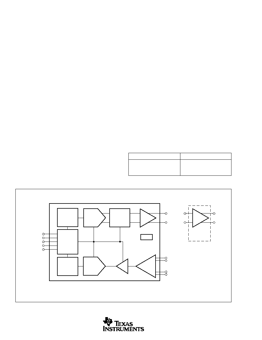
FIGURE 1. Functional Block Diagram of the AFE1230.
signal is processed by a sinc
5
filter as well as a programmable
IIR filter for droop compensation and additional quantization
noise reduction. The resulting digital signal is sent to the serial
interface for processing by the DSP.
Transmit Filter
The transmit filter consists of two sections, a digital interpo-
lation filter and a programmable SC low-pass filter (SCLPF).
The interpolation filter is an anti-imaging low-pass filter.
The SCLPF serves two important functions. First it is
designed to remove quantization noise from the delta-sigma
D/A converter in the front end of the transmit path. Sec-
ondly, the filter is used to help shape the received digital
signal's spectral density in conjunction with pre-spectral
shaping within the DSP. Depending on the particular re-
sponse desired, the transmit filter section can be programmed
for three different breakpoints, as shown in Table 1, as well
as two filter order (fifth or seventh) configurations. The 3dB
frequency listed in Table I is in relation to the designed
breakpoint for the SC filter only. However, because the
digital signal is sampled and held for 24 more samples (the
AFE1230 increases the sample rate by 24x in relation to the
input data rate), the actual transmit spectral curves contain a
small amount of droop due to the sinc function performed by
the sample and hold function of the delta-sigma modulator
section of the transmit path. See Figures 2 and 3 for the
overall spectral templates.
APPLICATION INFORMATION
THEORY OF OPERATION
The AFE1230 consists of a transmitter and receiver section, as
shown in Figure 1; the transmitter section consists of a digital
interpolation filter, a 16-bit, delta-sigma D/A converter, a
programmable fifth-order or seventh-order SC low-pass filter,
and a differential output line driver. The receiver section
includes a digitally programmable gain amplifier, a 16-bit,
delta-sigma A/D converter, and a decimation filter. The
AFE1230 receives a 16-bit word plus an 8-bit control byte via
the serial interface to facilitate the D/A conversion and control
functions. The received 16-bit word is up sampled by two
through the digital interpolation filter, then oversampled by
the delta-sigma modulator by a factor of 12x where it is then
processed by the multilevel D/A converter section before being
filtered by the fifth-order or seventh-order Butterworth low-
pass SC filter section.
The subsequent analog signal is sent to the on-chip line driver
where the analog signal can be driven into an appropriate
transformer to provide up to 14.5dBm power into a 135
line
for G.SHDSL. In addition, the on-chip line driver can be used
as an output buffer to generate 17dBm into a 135
line via an
external line driver (such as the OPA2677) for HDSL2. With an
appropriate DSP, the transmitted PSD complies with either the
G.SHDSL standard or, with an OPA2677 used as an external
driver, the HDSL2 standard.
In the receive path, the input amplifier sums the signals from the
line and hybrid paths to perform first-order analog echo cancel-
lation. The resultant signal is then digitized by a fourth-order
cascaded delta-sigma A/D converter with an OSR
(OverSampling Ratio) of 24x. The subsequent oversampled
TABLE I. tx Filter Cutoff Frequency Setting.
tx CUTOFF (txData Bits 29, 28)
RATIO (Corner Frequency)
00
0.25 MCLK/24
01
0.38 MCLK/24
10
0.5 MCLK/24
16-Bit
A/D Converter
PGA
Input
Amplifier
Patents Pending
AFE1230
Driver/
Buffer
txLINE
txLINE
hybINPUT
hybINPUT
rxINPUT
rxINPUT
OPA2677
tx and rx
Digital
Interface
Registers
Programmable
Digital
LPF
Digital
Interpolation
LPF
Programmable
SC
LPF
16-Bit
D/A Converter
MCLK
txBaud
txData
rxBaud
rxData
VrRef
External Driver
for HDSL2

AFE1230
5
SBWS015A
Receive Filter
The receive filter consists of three independent sections used
for both the removal of quantization noise as well as the
reduction of data rate (otherwise known as downsampling).
The first section is comprised of a sinc
5
filter with a
downsampling ratio of 12x. The resulting digital signal is then
passed to a droop compensation filter before being sent
through the final IIR filter section, while being downsampled
by two. Two filter cutoff configurations are available, as seen
in Table II. The corresponding cutoff frequencies relate to the
full-rate low-pass filter spectral template of the filter, as seen
from the inputs of Table II.
Transmit Power
The on-chip differential line driver is designed to drive G.SHDSL
power levels directly, or it can be used as a low-power buffer for
driving a higher power external driver (for example the OPA2677)
for applications such as HDSL2. The AFE1230 driver will
generate an output swing of 6.2V peak-to-peak differential.
When used with a suitable transformer (see Figures 8 and 10),
the AFE1230 can generate up to 14.5dBm of power into a 135
line load. When used as a buffer with an OPA2677 driver,
17dBm of power can be generated. Relative transmit power can
be controlled digitally through control bits sent to the transmit
section by the serial interface. Relative transmit power reduction
can be set to 0, ≠6, ≠12, or ≠18dB, depending on the control bits
presented to the AFE1230, as shown in Table III.
FIGURE 2. Overall Transmit Filter. D/A Converter Frequency Response, Fifth-Order with 0.25x, 0.38x, and 0.5x.
FIGURE 3. Overall Transmit Filter. D/A Converter Frequency Response, Seventh-Order with 0.25x, 0.38x, and 0.5x.
TABLE III. Transmit Power Backoff.
TABLE II. rx Filter Cutoff Frequency Setting.
rx CUTOFF (txData Bit 24)
RATIO (Corner Frequency)
0
0.25 MCLK/24
1
0.5 MCLK/24
TRANSMIT POWER
TRANSMIT
BACK OFF CODE
POWER
TRANSMIT POWER
(txData Bits 25, 26)
REDUCTION
G.SHDSL
HDSL2
00
0dB
14.5dBm
17.0dBm
01
≠6dB
8.5dBm
11.0dBm
10
≠12dB
2.5dBm
5.0dBm
11
≠18dB
≠4.5dBm
≠1.0dBm
0
≠50
≠100
≠150
≠200
≠250
≠300
10
≠3
10
≠2
10
≠1
10
0
0
≠50
≠100
≠150
≠200
≠250
≠300
≠350
10
≠3
10
≠2
10
≠1
10
0