Rev. 4135D�8051�08/05
1
Features
�
Pin and Software Compatibility with Standard 80C51 Products and 80C51Fx/Rx/Rx+
�
Plug-In Replacement of Intel's 8xC251Sx
�
C251 Core: Intel's MCS
�
251 D-step Compliance
�
40-byte Register File
�
Registers Accessible as Bytes, Words or Dwords
�
Three-stage Instruction Pipeline
�
16-bit Internal Code Fetch
�
Enriched C51 Instruction Set
�
16-bit and 32-bit ALU
�
Compare and Conditional Jump Instructions
�
Expanded Set of Move Instructions
�
Linear Addressing
�
1 Kbyte of On-Chip RAM
�
External Memory Space (Code/Data) Programmable from 64 kilobytes to 256 kilobytes
�
TSC87251G2D: 32 kilobytes of On-Chip EPROM/OTPROM
� SINGLE PULSE Programming Algorithm
�
TSC83251G1D: 16 kilobytes of On-Chip Masked ROM
�
TSC83251G1D: 32 kilobytes of On-Chip Masked ROM
�
TSC80251G1D: ROMless Version
�
Four 8-bit Parallel I/O Ports (Ports 0, 1, 2 and 3 of the Standard 80C51)
�
Serial I/O Port: Full Duplex UART (80C51 Compatible) With Independent Baud Rate
Generator
�
SSLC: Synchronous Serial Link Controller
�
TWI Multi-master Protocol
�
Wire and SPI Master and Slave Protocols
�
Three 16-bit Timers/Counters (Timers 0, 1 and 2 of the Standard 80C51)
�
EWC: Event and Waveform Controller
�
Compatible with Intel's Programmable Counter Array (PCA)
�
Common 16-bit Timer/Counter Reference with Four Possible Clock Sources (Fosc/4,
Fosc/12, Timer 1 and External Input)
�
Five Modules, Each with Four Programmable Modes:
� 16-bit Software Timer/Counter
� 16-bit Timer/Counter Capture Input and Software Pulse Measurement
� High-speed Output and 16-bit Software Pulse Width Modulation (PWM)
� 8-bit Hardware PWM Without Overhead
�
16-bit Watchdog Timer/Counter Capability
�
Secure 14-bit Hardware Watchdog Timer
�
Power Management
�
Power-On Reset (Integrated on the Chip)
�
Power-Off Flag (Cold and Warm Resets)
�
Software Programmable System Clock
�
Idle Mode
�
Power-down Mode
�
Keyboard Interrupt Interface on Port 1
�
Non Maskable Interrupt Input (NMI)
�
Real-Time Wait States Inputs (WAIT#/AWAIT#)
�
ONCE Mode and Full Speed Real-time In-circuit Emulation Support (Third Party
Vendors)
�
High Speed Versions:
� 4.5V to 5.5V
� 16 MHz and 24 MHz
�
Typical Operating Current: 35 mA at 24 MHz
24 mA at 16 MHz
�
Typical Power-down Current: 2
A
�
Low Voltage Version:
� 2.7V to 5.5V
� 16 MHz
8/16-bit
Microcontroller
with Serial
Communication
Interfaces
TSC80251G2D
TSC83251G2D
TSC87251G2D
AT80251G2D
AT83251G2D
AT87251G2D

2
AT/TSC8x251G2D
4135D�8051�08/05
�
Typical Operating Current:11 mA at 3V
�
Typical Power-down Current: 1
A
�
Temperature Ranges: Commercial (0
�
C to +70
�
C), Industrial (-40
�
C to +85
�
C)
�
Option: Extended Range (-55
�
C to +125
�
C)
�
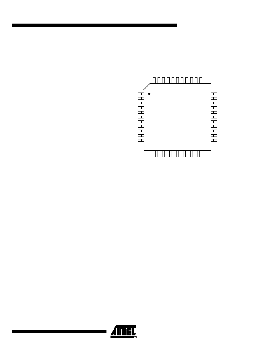
Packages: PDIL 40, PLCC 44 and VQFP 44, CDIL 40 and CQPJ 44 with Window
�
Options: Known Good Dice and Ceramic Packages
Description
The TSC80251G2D products are derivatives of the Atmel Microcontroller family based on the 8/16-bit C251 Architecture.
This family of products is tailored to 8/16-bit microcontroller applications requiring an increased instruction throughput, a
reduced operating frequency or a larger addressable memory space. The architecture can provide a significant code size
reduction when compiling C programs while fully preserving the legacy of C51 assembly routines.
The TSC80251G2D derivatives are pin and software compatible with standard 80C51/Fx/Rx/Rx+ with extended on-chip
data memory (1 Kbyte RAM) and up to 256 kilobytes of external code and data. Additionally, the TSC83251G2D and
TSC87251G2D provide on-chip code memory: 32 kilobytes ROM and 32 kilobytes EPROM/OTPROM respectively.
They provide transparent enhancements to Intel's 8xC251Sx family with an additional Synchronous Serial Link Controller
(SSLC supporting TWI,
Wire and SPI protocols), a Keyboard interrupt interface, a dedicated Baud Rate Generator for
UART, and Power Management features.
TSC80251G2D derivatives are optimized for speed and for low power consumption on a wide voltage range.
Note:
1. This Datasheet provides the technical description of the TSC80251G2D derivatives. For further information on the device
usage, please request the TSC80251 Programmer's Guide and the TSC80251G1D Design Guide and errata sheet.
Typical Applications
�
ISDN Terminals
�
High-Speed Modems
�
PABX (SOHO)
�
Line Cards
�
DVD ROM and Players
�
Printers
�
Plotters
�
Scanners
�
Banking Machines
�
Barcode Readers
�
Smart Cards Readers
�
High-End Digital Monitors
�
High-End Joysticks
�
High-end TV's