 | –≠–Ľ–Ķ–ļ—ā—Ä–ĺ–Ĺ–Ĺ—č–Ļ –ļ–ĺ–ľ–Ņ–ĺ–Ĺ–Ķ–Ĺ—ā: TH7814A | –°–ļ–į—á–į—ā—Ć:  PDF PDF  ZIP ZIP |

1
Features
∑
Data Rate up to 50 MHz (2 Outputs at 25 MHz Each)
∑
Pixel Size: 10 Ķm x 10 Ķm (10 Ķm Pitch)
∑
300 to 1100 nm Spectral Range
∑
High Sensitivity and Lag-free Photodiodes
∑
Very Low Noise (30 pJ/cm
2
Noise Equivalent Illumination)
∑
Antiblooming
∑
Exposure Control
∑
20-lead 0.4" DIL Package
∑
Electrical, Mechanical and Optical Compatibility Between the Two Products
The TH7813 and TH7814 linear arrays are based on Atmel's most recent know-how in
terms of design and technology. Flexibility and performance of these devices give the
opportunity to use them in most vision systems for industrial applications (web inspec-
tion, process control, sorting and inspection of various parts), document scanning up
to 200 dpi, metrology, etc.
Pin Identification
All pins must be connected
Pin Number
Symbol
Function
4, 17
VDD1,2
Output Amplifiers Drain Supply
3, 18
VOS1,2
Video Outputs
5
VS
Output Amplifiers Substrate Bias
20
VDR
Reset Drain Supply
2
VGS
Output Gate Bias
14
L1
Readout Register Clocks
13
L2
15
R
Reset Clock
10
A
Antiblooming Gate Bias/Clock
7
VA
Antiblooming Drain Bias
8
VST
Storage Gate Bias
11
P
Transfer Gate Clock
1, 6, 9, 12, 16, 19
VSS
Ground, Optical Shield Grounding
(Internally Connected)
1
2
3
4
5
6
7
8
9
10
20
19
18
17
16
15
14
13
12
11
VSS
VGS
VOS1
VDD1
VS
VSS
VA
VST
VSS
A
VDR
VSS
VOS2
VDD2
VSS
R
L1
L2
VSS
P
TH7813A
TH7814A
50 MHz
1024/2048
Linear CCDs
TH7813A
TH7814A
Rev. 1990A≠IMAGE≠05/02

2
TH7813A/TH7814A
1990A≠IMAGE≠05/02
Note:
Operating range defines the limits within which the functionality is guaranteed.
Electrical limits of applied signals are given in operating conditions section.
Operating Precautions
Shorting the video outputs to any other pin, even temporarily, can permanently damage
the on-chip output amplifier.
Operating Conditions
Absolute Maximum Ratings*
Storage Temperature Range ......................... -55įC to +150įC
*NOTICE:
Stresses above those listed under absolute max-
imum ratings may cause permanent device fail-
ure. Functionality at or above these limits is not
implied. Exposure to absolute maximum ratings
for extended periods may affect device reliability.
Operating Temperature Range........................ -40įC to +85įC
Thermal Cycling..........................................................15įC/mn
Maximum Applied Voltages:
∑ Pin: 2, 8, 10, 11, 13, 14, 15 .................................. -0.3 to 15V
∑ Pin: 4, 5, 7, 17, 20 ................................................ -0.3 to 16V
∑ Pin: 1, 6, 9, 12, 16, 19 .........................................0V (ground)
Table 1. DC Characteristics
Parameter
Symbol
Value
Unit
Min
Typ
Max
Output Amplifier Drain Supply
VDD1, VDD2
14.5
15
15.5
V
Storage Gate Bias
VST
2.2
2.4
2.6
V
Antiblooming Gate (See Pixel
Saturation Adjustment)
A
2
4
7
V
Reset Bias
VDR
13.5
14
14.5
V
Antiblooming Diode Bias
VA
14.5
15
15.5
V
3
TH7813A/TH7814A
1990A≠IMAGE≠05/02
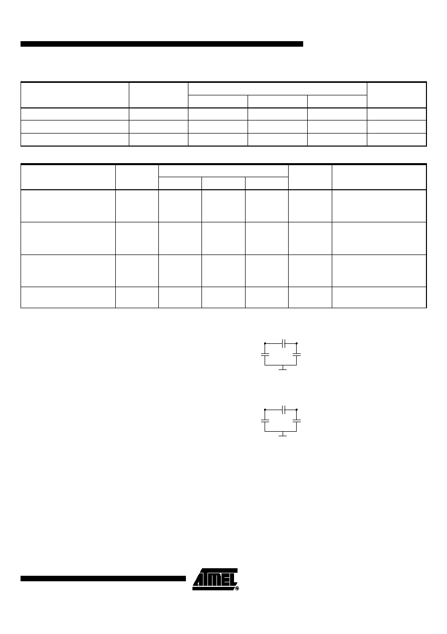
Figure 1. Readout Register Clocks Capacitance TH7813
Figure 2. Readout Register Clocks Capacitance TH7814
Register Output Gate Bias
VGS
2.2
2.4
2.6
V
Output Amplifier Source Supply
VS
0
V
Ground
VSS
0
Table 2. Drive Clocks Characteristics
Parameter
Symbol
Value
Unit
Remark
Min.
Typ.
Max.
Reset gate
High level
Low level
R
8.5
-0.1
9
0
9.5
0.4
V
V
Clock Capacitance < 25 pF
Transfer gate
High level
Low level
P
8.5
-0.1
9
0
9.5
0.4
V
V
Clock Capacitance < 100 pF
Readout register clocks
Hilgh level
Low level
L1, 2
8.5
-0.1
9
0
9.5
0.4
V
V
see Figure 1 and Figure 2
Maximum readout register
frequency
F
H
10
25
MHz
Table 1. DC Characteristics (Continued)
Parameter
Symbol
Value
Unit
Min
Typ
Max
50 pF
140 pF
120 pF
L1
L2
100 pF
230 pF
230 pF
L1
L2

4
TH7813A/TH7814A
1990A≠IMAGE≠05/02
Timing Diagrams
The following diagram shows the general clocking scheme for the TH7813A and
TH7814A.
The line is composed as follows:
Postscan elements may be added in order to either increase the exposure time, or to
provide a voltage reference level.
Figure 3. Line Timing Diagram
The following diagram shows the timing for the transfer period:
Figure 4. Line Transfer Period
R clock may also be held in high state during line transfer period.
The following diagram shows the detailed timing for the pixel readout:
Synopsis
Number of Prescan
Pixels Per Output
Number of Useful
Pixels Per Output
Total Number of
Pixels Per Output
TH7813A
4
512
516
TH7814A
4
1024
1028
A
P
L1
L2
R
Line Period
Transfer Period
A
P
L1
L2
R
> 300 ns
> 10 ns
> 10 ns
first prescan pixel
(700 ns typ.)

5
TH7813A/TH7814A
1990A≠IMAGE≠05/02
Figure 5. Pixel Readout Timing Diagram
Exposure Time
Reduction
The antiblooming structure of the TH7813A and TH7814A provides an electronic shutter
capability by clocking phase fA during the line period. The timing diagram is described
below:
Note:
Clock capacitance: TH7813A = 50 pF, TH7814A = 100 pF
L1
L2
R
10%
90%
90%
10%
tr
tf
Tpixel
0 ns
10 ns
50%
Video signal
Reset Feedthrough
Offset in darkness
VIDEO OUTPUTS
Ī
floating diode level
Duty cycle: 50%
Ī
10%
Crossover at 50%
Ī
10%
Rise and fall time
10 ns
Rise and fall time
8 ns
Video outputs are synchronous
Video signal occurs on L2 falling edge
First useful pixel occurs on 5th
falling edge of L2 after P
Antiblooming Gate
A
Min
Typ
Max
Unit
Clock Capacitance (see note)
High Level
8.5
9
9.5
V
Low Level Sets Saturation Level
Low Level
2
4
7
V
See Pixel Saturation Adjustment
Pulse Min.
200
ns