2514J≠AVR≠12/03
Features
∑
High Performance, Low Power AVR
Æ
8-Bit Microcontroller
∑
Advanced RISC Architecture
≠ 130 Powerful Instructions ≠ Most Single Clock Cycle Execution
≠ 32 x 8 General Purpose Working Registers
≠ Fully Static Operation
≠ Up to 16 MIPS Throughput at 16 MHz
≠ On-Chip 2-cycle Multiplier
∑
Non-volatile Program and Data Memories
≠ 16K bytes of In-System Self-Programmable Flash
Endurance: 10,000 Write/Erase Cycles
≠ Optional Boot Code Section with Independent Lock Bits
In-System Programming by On-chip Boot Program
True Read-While-Write Operation
≠ 512 bytes EEPROM
Endurance: 100,000 Write/Erase Cycles
≠ 1K byte Internal SRAM
≠ Programming Lock for Software Security
∑
JTAG (IEEE std. 1149.1 compliant) Interface
≠ Boundary-scan Capabilities According to the JTAG Standard
≠ Extensive On-chip Debug Support
≠ Programming of Flash, EEPROM, Fuses, and Lock Bits through the JTAG Interface
∑
Peripheral Features
≠ 4 x 25 Segment LCD Driver
≠ Two 8-bit Timer/Counters with Separate Prescaler and Compare Mode
≠ One 16-bit Timer/Counter with Separate Prescaler, Compare Mode, and Capture
Mode
≠ Real Time Counter with Separate Oscillator
≠ Four PWM Channels
≠ 8-channel, 10-bit ADC
≠ Programmable Serial USART
≠ Master/Slave SPI Serial Interface
≠ Universal Serial Interface with Start Condition Detector
≠ Programmable Watchdog Timer with Separate On-chip Oscillator
≠ On-chip Analog Comparator
≠ Interrupt and Wake-up on Pin Change
∑
Special Microcontroller Features
≠ Power-on Reset and Programmable Brown-out Detection
≠ Internal Calibrated Oscillator
≠ External and Internal Interrupt Sources
≠ Five Sleep Modes: Idle, ADC Noise Reduction, Power-save, Power-down, and
Standby
∑
I/O and Packages
≠ 53 Programmable I/O Lines
≠ 64-lead TQFP and 64-pad MLF
∑
Operating Voltage:
≠ 1.8 - 5.5V for ATmega169V
≠ 2.7 - 5.5V for ATmega169L
≠ 4.5 - 5.5V for ATmega169
∑
Temperature range:
≠ -40∞C to 85∞C Industrial
8-bit
Microcontroller
with 16K Bytes
In-System
Programmable
Flash
ATmega169V
ATmega169L
ATmega169
Preliminary
2
ATmega169V/L
2514J≠AVR≠12/03
Features (Continued)
∑
Speed Grade:
≠ 0 - 1 MHz for ATmega169V
≠ 0 - 8 MHz for ATmega169L
≠ 0 - 16 MHz for ATmega169
∑
Ultra-Low Power Consumption
≠ Active Mode:
1 MHz, 1.8V: 400µA
32 kHz, 1.8V: 20µA (including Oscillator)
32 kHz, 1.8V: 40µA (including Oscillator and LCD)
≠ Power-down Mode:
0.5µA at 1.8V
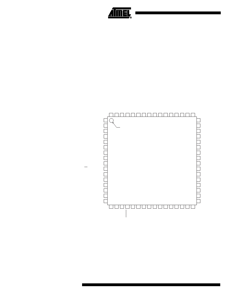
Pin Configurations
Figure 1. Pinout ATmega169
Disclaimer
Typical values contained in this datasheet are based on simulations and characteriza-
tion of other AVR microcontrollers manufactured on the same process technology. Min
and Max values will be available after the device is characterized.
PC0 (SEG12)
VCC
GND
PF0 (ADC0)
PF7 (ADC7/TDI)
PF1 (ADC1)
PF2 (ADC2)
PF3 (ADC3)
PF4 (ADC4/TCK)
PF5 (ADC5/TMS)
PF6 (ADC6/TDO)
AREF
GND
AVCC
17
61
60
18
59
20
58
19
21
57
22
56
23
55
24
54
25
53
26
52
27
51
29
28
50
49
32
31
30
(RXD/PCINT0) PE0
(TXD/PCINT1) PE1
LCDCAP
(XCK/AIN0/PCINT2) PE2
(AIN1/PCINT3) PE3
(USCK/SCL/PCINT4) PE4
(DI/SDA/PCINT5) PE5
(DO/PCINT6) PE6
(CLKO/PCINT7) PE7
(SS/PCINT8) PB0
(SCK/PCINT9) PB1
(MOSI/PCINT10) PB2
(MISO/PCINT11) PB3
(OC0A/PCINT12) PB4
(OC2A/PCINT15) PB7
(T1/SEG24) PG3
(OC1B/PCINT14) PB6
(T0/SEG23) PG4
(OC1A/PCINT13) PB5
PC1 (SEG11)
PG0 (SEG14)
(SEG15) PD7
PC2 (SEG10)
PC3 (SEG9)
PC4 (SEG8)
PC5 (SEG7)
PC6 (SEG6)
PC7 (SEG5)
PA7 (SEG3)
PG2 (SEG4)
PA6 (SEG2)
PA5 (SEG1)
PA4 (SEG0)
PA3 (COM3)
PA0 (COM0)
PA1 (COM1)
PA2 (COM2)
PG1 (SEG13)
(SEG16) PD6
(SEG17) PD5
(SEG18) PD4
(SEG19) PD3
(SEG20) PD2
(INT0/SEG21) PD1
(ICP1/SEG22) PD0
(TOSC1) XTAL1
(TOSC2) XTAL2
RESET
GND
VCC
ATmega169
INDEX CORNER
2
3
1
4
5
6
7
8
9
10
11
12
13
14
16
15
64
63
62
47
46
48
45
44
43
42
41
40
39
38
37
36
35
33
34

4
ATmega169V/L
2514J≠AVR≠12/03
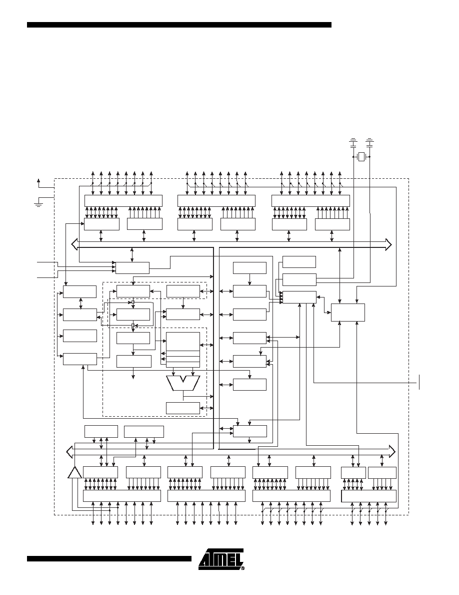
The AVR core combines a rich instruction set with 32 general purpose working registers.
All the 32 registers are directly connected to the Arithmetic Logic Unit (ALU), allowing
two independent registers to be accessed in one single instruction executed in one clock
cycle. The resulting architecture is more code efficient while achieving throughputs up to
ten times faster than conventional CISC microcontrollers.
The ATmega169 provides the following features: 16K bytes of In-System Programmable
Flash with Read-While-Write capabilities, 512 bytes EEPROM, 1K byte SRAM,
53 general purpose I/O lines, 32 general purpose working registers, a JTAG interface
for Boundary-scan, On-chip Debugging support and programming, a complete On-chip
LCD controller with internal step-up voltage, three flexible Timer/Counters with compare
modes, internal and external interrupts, a serial programmable USART, Universal Serial
Interface with Start Condition Detector, an 8-channel, 10-bit ADC, a programmable
Watchdog Timer with internal Oscillator, an SPI serial port, and five software selectable
power saving modes. The Idle mode stops the CPU while allowing the SRAM,
Timer/Counters, SPI port, and interrupt system to continue functioning. The Power-
down mode saves the register contents but freezes the Oscillator, disabling all other
chip functions until the next interrupt or hardware reset. In Power-save mode, the asyn-
chronous timer and the LCD controller continues to run, allowing the user to maintain a
timer base and operate the LCD display while the rest of the device is sleeping. The
ADC Noise Reduction mode stops the CPU and all I/O modules except asynchronous
timer, LCD controller and ADC, to minimize switching noise during ADC conversions. In
Standby mode, the crystal/resonator Oscillator is running while the rest of the device is
sleeping. This allows very fast start-up combined with low-power consumption.
The device is manufactured using Atmel's high density non-volatile memory technology.
The On-chip ISP Flash allows the program memory to be reprogrammed In-System
through an SPI serial interface, by a conventional non-volatile memory programmer, or
by an On-chip Boot program running on the AVR core. The Boot program can use any
interface to download the application program in the Application Flash memory. Soft-
ware in the Boot Flash section will continue to run while the Application Flash section is
updated, providing true Read-While-Write operation. By combining an 8-bit RISC CPU
with In-System Self-Programmable Flash on a monolithic chip, the Atmel ATmega169 is
a powerful microcontroller that provides a highly flexible and cost effective solution to
many embedded control applications.
The ATmega169 AVR is supported with a full suite of program and system development
tools including: C Compilers, Macro Assemblers, Program Debugger/Simulators, In-Cir-
cuit Emulators, and Evaluation kits.

5
ATmega169V/L
2514J≠AVR≠12/03
Pin Descriptions
VCC
Digital supply voltage.
GND
Ground.
Port A (PA7..PA0)
Port A is an 8-bit bi-directional I/O port with internal pull-up resistors (selected for each
bit). The Port A output buffers have symmetrical drive characteristics with both high sink
and source capability. As inputs, Port A pins that are externally pulled low will source
current if the pull-up resistors are activated. The Port A pins are tri-stated when a reset
condition becomes active, even if the clock is not running.
Port A also serves the functions of various special features of the ATmega169 as listed
on page 59.
Port B (PB7..PB0)
Port B is an 8-bit bi-directional I/O port with internal pull-up resistors (selected for each
bit). The Port B output buffers have symmetrical drive characteristics with both high sink
and source capability. As inputs, Port B pins that are externally pulled low will source
current if the pull-up resistors are activated. The Port B pins are tri-stated when a reset
condition becomes active, even if the clock is not running.
Port B has better driving capabilities than the other ports.
Port B also serves the functions of various special features of the ATmega169 as listed
on page 60.
Port C (PC7..PC0)
Port C is an 8-bit bi-directional I/O port with internal pull-up resistors (selected for each
bit). The Port C output buffers have symmetrical drive characteristics with both high sink
and source capability. As inputs, Port C pins that are externally pulled low will source
current if the pull-up resistors are activated. The Port C pins are tri-stated when a reset
condition becomes active, even if the clock is not running.
Port C also serves the functions of special features of the ATmega169 as listed on page
63.
Port D (PD7..PD0)
Port D is an 8-bit bi-directional I/O port with internal pull-up resistors (selected for each
bit). The Port D output buffers have symmetrical drive characteristics with both high sink
and source capability. As inputs, Port D pins that are externally pulled low will source
current if the pull-up resistors are activated. The Port D pins are tri-stated when a reset
condition becomes active, even if the clock is not running.
Port D also serves the functions of various special features of the ATmega169 as listed
on page 65.
Port E (PE7..PE0)
Port E is an 8-bit bi-directional I/O port with internal pull-up resistors (selected for each
bit). The Port E output buffers have symmetrical drive characteristics with both high sink
and source capability. As inputs, Port E pins that are externally pulled low will source
current if the pull-up resistors are activated. The Port E pins are tri-stated when a reset
condition becomes active, even if the clock is not running.
Port E also serves the functions of various special features of the ATmega169 as listed
on page 67.
Port F (PF7..PF0)
Port F serves as the analog inputs to the A/D Converter.
Port F also serves as an 8-bit bi-directional I/O port, if the A/D Converter is not used.
Port pins can provide internal pull-up resistors (selected for each bit). The Port F output