Features
�
High Performance, Low Power AVR
�
8-Bit Microcontroller
�
Advanced RISC Architecture
� 135 Powerful Instructions � Most Single Clock Cycle Execution
� 32 x 8 General Purpose Working Registers
� Fully Static Operation
� Up to 16 MIPS Throughput at 16 MHz
� On-Chip 2-cycle Multiplier
�
Non-volatile Program and Data Memories
� 64/128K Bytes of In-System Self-Programmable Flash
� Endurance: 100,000 Write/Erase Cycles
� Optional Boot Code Section with Independent Lock Bits
� In-System Programming by On-chip Boot Program hardware activated after
reset
� True Read-While-Write Operation
� 2K/4K (64K/128K Flash version) Bytes EEPROM
� Endurance: 100,000 Write/Erase Cycles
� 4K/8K (64K/128K Flash version) Bytes Internal SRAM
� Up to 64K Bytes Optional External Memory Space
� Programming Lock for Software Security
�
JTAG (IEEE std. 1149.1 compliant) Interface
� Boundary-scan Capabilities According to the JTAG Standard
� Extensive On-chip Debug Support
� Programming of Flash, EEPROM, Fuses, and Lock Bits through the JTAG Interface
�
USB 2.0 Full-speed/Low-speed Device and On-The-Go Module
� Complies fully with:
� Universal Serial Bus Specification REV 2.0
� On-The-Go Supplement to the USB 2.0 Specification Rev 1.0
� Supports data transfer rates up to 12 Mbit/s and 1.5 Mbit/s
�
USB Full-speed/Low Speed Device Module with Interrupt on Transfer Completion
� Endpoint 0 for Control Transfers : up to 64-bytes
� 6 Programmable Endpoints with IN or Out Directions and with Bulk, Interrupt or
Isochronous Transfers
� Configurable Endpoints size up to 256 bytes in double bank mode
� Fully independant 832 bytes USB DPRAM for endpoint memory allocation
� Suspend/Resume Interrupts
� Power-on Reset and USB Bus Reset
� 48 MHz PLL for Full-speed Bus Operation
� USB Bus Disconnection on Microcontroller Request
�
USB OTG:
� Supports Host Negotiation Protocol (HNP) and Session Request Protocol (SRP)
for OTG dual-role devices
� Provide Status and control signals for software implementation of HNP and SRP
� Provides programmable times required for HNP and SRP
�
Peripheral Features
� Two 8-bit Timer/Counters with Separate Prescaler and Compare Mode
� Two16-bit Timer/Counter with Separate Prescaler, Compare- and Capture Mode
� Real Time Counter with Separate Oscillator
� Two 8-bit PWM Channels
8-bit
Microcontroller
with
64/128K Bytes
of ISP Flash
and USB
Controller
AT90USB646
AT90USB647
AT90USB1286
AT90USB1287
Preliminary

2
7593A�AVR�02/06
AT90USB64/128
� Six PWM Channels with Programmable Resolution from 2 to 16 Bits
� Output Compare Modulator
� 8-channels, 10-bit ADC
� Programmable Serial USART
� Master/Slave SPI Serial Interface
� Byte Oriented 2-wire Serial Interface
� Programmable Watchdog Timer with Separate On-chip Oscillator
� On-chip Analog Comparator
� Interrupt and Wake-up on Pin Change
�
Special Microcontroller Features
� Power-on Reset and Programmable Brown-out Detection
� Internal Calibrated Oscillator
� External and Internal Interrupt Sources
� Six Sleep Modes: Idle, ADC Noise Reduction, Power-save, Power-down, Standby, and Extended Standby
�
I/O and Packages
� 48 Programmable I/O Lines
� 64-lead TQFP and 64-lead QFN
�
Operating Voltages
� 2.7 - 5.5V
� 2.2 - 5.5V (Check availabilty)
�
Operating temperature
� Industrial (-40�C to +85�C)
�
Maximum Frequency
� 8 MHz at 2.7V - Industrial range
� 16 MHz at 4.5V - Industrial range
4
7593A�AVR�02/06
AT90USB64/128
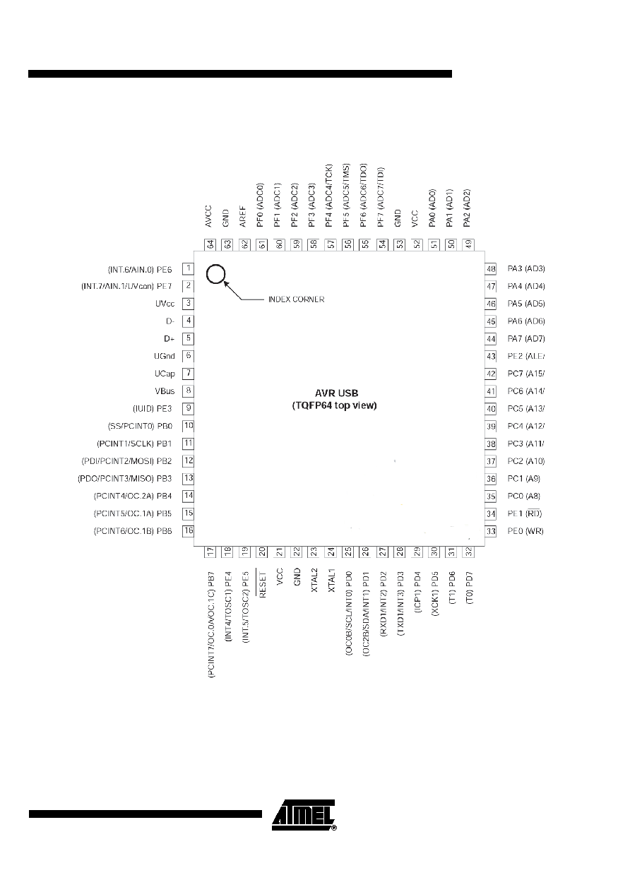
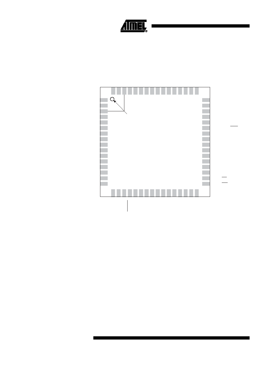
Figure 1-2.
Pinout AT90USB64/128-QFN
Note:
The large center pad underneath the MLF packages is made of metal and internally connected to
GND. It should be soldered or glued to the board to ensure good mechanical stability. If the center
pad is left unconnected, the package might loosen from the board.
1.1
Disclaimer
Typical values contained in this datasheet are based on simulations and characterization of
other AVR microcontrollers manufactured on the same process technology. Min and Max values
will be available after the device is characterized.
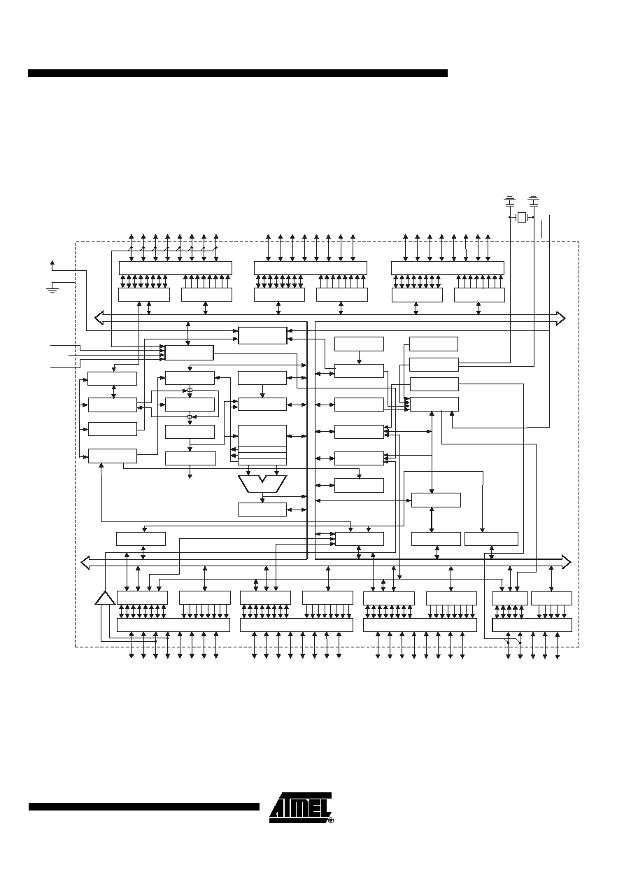
2. Overview
The AT90USB64/128 is a low-power CMOS 8-bit microcontroller based on the AVR enhanced
RISC architecture. By executing powerful instructions in a single clock cycle, the
2
3
1
4
5
6
7
8
9
10
11
12
13
14
16
33
15
47
46
48
45
44
43
42
41
40
39
38
37
36
35
34
17
18
20
19
21
22
23
24
25
26
27
29
28
32
31
30
52
51
50
49
64
63
62
53
61
60
59
58
57
56
55
54
AT90USB128
(64-lead QFN top view)
INDEX CORNER
A
VCC
GND
AREF
PF0 (ADC0)
PF1 (ADC1)
PF2 (ADC2)
PF3 (ADC3)
PF4 (ADC4/TCK
)
PF5 (ADC5/TMS
)
PF6 (ADC6/TDO
)
PF7 (ADC7/TDI)
GND
VCC
P
A0 (AD0)
P
A1 (AD1)
P
A2 (AD2)
(INT.7/AIN.1/UVcon) PE7
UVcc
D-
D+
UGnd
UCap
VBus
(IUID) PE3
(SS/PCINT0) PB0
(INT.6/AIN.0) PE6
(PCINT1/SCLK) PB1
(PDI/PCINT2/MOSI) PB2
(PDO/PCINT3/MISO) PB3
(PCINT4/OC.2A) PB4
(PCINT5/OC.1A) PB5
(PCINT6/OC.1B) PB6
(
PCINT7/OC.0A/OC.1C) PB7
(INT4/T
OSC1) PE4
(INT
.5/T
OSC2) PE5
VCC
GND
XT
AL2
XT
AL1
(OC0B/SCL/INT0) PD0
(OC2B/SDA/INT1) PD1
(RXD1/INT2) PD2
(TXD1/INT3) PD3
(ICP1) PD4
(XCK1) PD5
(T1) PD6
(T0) PD7
RESET
PA3 (AD3)
PA4 (AD4)
PA5 (AD5)
PA6 (AD6)
PA7 (AD7)
PE2 (ALE/HWB)
PC7 (A15/IC.3/CLK0)
PC6 (A14/OC.3A)
PC5 (A13/OC.3B)
PC4 (A12/OC.3C)
PC3 (A11/T.3)
PC2 (A10)
PC1 (A9)
PC0 (A8)
PE1 (RD)
PE0 (WR)