
1
Features
∑
Utilizes the AVR
Æ
RISC Architecture
∑
AVR ≠ High-performance and Low-power RISC Architecture
≠ 118 Powerful Instructions ≠ Most Single Clock Cycle Execution
≠ 32 x 8 General-purpose Working Registers
≠ Up to 1.5 MIPS Throughput at 1.5 MHz
∑
Data and Nonvolatile Program Memory
≠ 8K Bytes Flash Program Memory
Endurance: 1,000 Write/Erase Cycles
≠ 256 Bytes Internal SRAM
≠ 512 Bytes EEPROM
Endurance: 100,000 Write/Erase Cycles
≠ Programming Lock for Flash Program and EEPROM Data Security
∑
Peripheral Features
≠ One 8-bit Timer/Counter with Separate Prescaler
≠ One 16-bit Timer/Counter with Separate Prescaler
∑
Special Microcontroller Features
≠ Low-power Idle and Power-down Modes
≠ External and Internal Interrupt Sources
≠ 6-channel, 10-bit ADC
∑
Specifications
≠ Low-power, High-speed CMOS Process Technology
≠ Fully Static Operation
∑
Power Consumption at 1.5 MHz, 3.6V, 25
∞C
≠ Active: 1.2 mA
≠ Idle Mode: 0.2 mA
≠ Power-down Mode: <10 µA
∑
I/O and Packages
≠ Seven General Output Lines
≠ Two External Interrupt Lines
≠ 48-lead LQFP/VQFP Package
∑
Operating Voltage
≠ 3.3 - 6.0V
∑
Speed Grade
≠ 0 - 1.5 MHz
Description
The AT90C8534 is a low-power CMOS 8-bit microcontroller based on the AVR RISC
architecture. By executing powerful instructions in a single clock cycle, the
Rev. 1229BS≠11/00
8-bit
Microcontroller
with 8K Bytes
Programmable
Flash
AT90C8534
Preliminary
Pin Configuration
1
2
3
4
5
6
7
8
9
10
11
12
36
35
34
33
32
31
30
29
28
27
26
25
ADIN0
NC
NC
NC
NC
NC
NC
NC
NC
NC
AGND
NC
NC
INT0
INT1
PA6
NC
GND
NC
NC
NC
NC
NC
NC
48
47
46
45
44
43
42
41
40
39
38
37
13
14
15
16
17
18
19
20
21
22
23
24
ADIN1
ADIN2
ADIN3
ADIN4
ADIN5
AVCC
NC
RESET
NC
VCC
XTAL2
XTAL1
NC
PA0
PA1
PA2
PA3
NC
NC
NC
NC
PA4
PA5
NC
(continued)
Note: This is a summary document. A complete document is
available on our web site at www.atmel.com.
AT90C8534
2
AT90C8534 achieves throughputs approaching 1 MIPS per MHz allowing the system designer to optimize power consump-
tion versus processing speed.
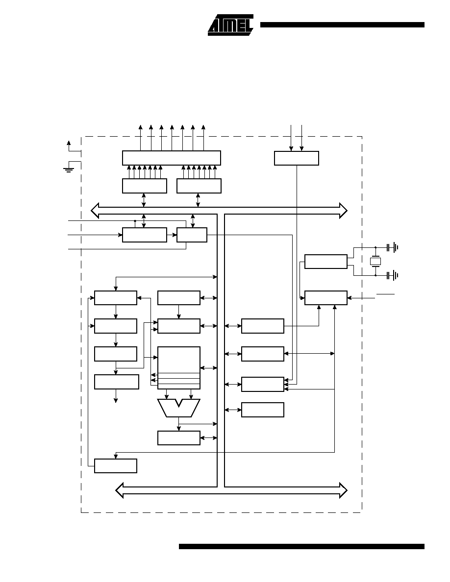
Block Diagram
Figure 1. The AT90C8534 Block Diagram
PROGRAM
COUNTER
STACK
POINTER
PROGRAM
FLASH
MCU CONTROL
REGISTER
SRAM
GENERAL
PURPOSE
REGISTERS
INSTRUCTION
REGISTER
TIMER/
COUNTERS
INSTRUCTION
DECODER
DATA DIR.
REG. PORTA
DATA REGISTER
PORTA
ANALOG MUX
ADC
PROGRAMMING
LOGIC
TIMING AND
CONTROL
OSCILLATOR
INTERRUPT
UNIT
EEPROM
STATUS
REGISTER
Z
Y
X
ALU
PORTA DRIVERS
PA0 - PA6
RESET
VCC
AVCC
AGND
GND
XTAL2
XTAL1
CONTROL
LINES
8-BIT DATA BUS
ADIN5..0
EXTERNAL
INTERRUPTS
INT1,0

AT90C8534
3
The AVR core combines a rich instruction set with 32 general-purpose working registers. All the 32 registers are directly
connected to the Arithmetic Logic Unit (ALU), allowing two independent registers to be accessed in one single instruction
executed in one clock cycle. The resulting architecture is more code efficient while achieving throughputs up to ten times
faster than conventional CISC microcontrollers.
The AT90C8534 provides the following features: 8K bytes of programmable Flash, 512 bytes EEPROM, 256 bytes SRAM,
7 general output lines, 2 external interrupt lines, 32 general-purpose working registers, 2 flexible timer/counters, internal
and external interrupts, 6-channel, 10-bit ADC, and 2 software-selectable power saving modes. The Idle mode stops the
CPU while allowing the ADC, timer/counters and interrupt system to continue functioning. The Power-down mode saves
the SRAM and register contents but freezes the oscillator, disabling all other chip functions until the next interrupt or hard-
ware reset.
The device is manufactured using Atmel's high-density nonvolatile memory technology. The on-chip programmable Flash
allows the program memory to be reprogrammed by a conventional nonvolatile memory programmer. By combining an
8-bit RISC CPU with programmable Flash on a monolithic chip, the Atmel AT90C8534 is a powerful microcontroller that
provides a highly flexible and cost-effective solution to many embedded control applications.
The AT90C8534 AVR is supported with a full suite of program and system development tools including: C compilers, macro
assemblers, program debugger/simulators, in-circuit emulators and evaluation kits.
Pin Descriptions
VCC
Digital supply voltage
GND
Digital ground
Port A (PA6..PA0)
Port A is a 7-bit output port with tri-state mode. The Port A output buffers can sink 20 mA and can drive LED displays
directly. The port pins are tri-stated when a reset condition becomes active, even if the clock is not running.
INT1, 0
External interrupt input pins. A falling or rising edge on either of these pins will generate an interrupt request. Interrupt
pulses longer than 40 ns will generate an interrupt, even if the clock is not running.
ADIN5..0
ADC input pins. Any of these pins can be selected as the input to the ADC.
RESET
Reset input. An external reset is generated by a low level on the RESET pin. Reset pulses longer than 100 ns will generate
a reset, even if the clock is not running. Shorter pulses are not guaranteed to generate a reset.
XTAL1
Input to the inverting oscillator amplifier and input to the internal clock operating circuit.
XTAL2
Output from the inverting oscillator amplifier
AVCC
This is the supply voltage pin for the A/D Converter. If the ADC is not used, the pin must be connected to V
CC
. If the ADC is
used, the pin should be connected to VCC via a low-pass filter.
AGND
Analog ground. If the board has a separate analog ground plane, this pin should be connected to this ground plane.
Otherwise, connect to GND.

AT90C8534
4
Architectural Overview
The fast-access register file concept contains 32 x 8-bit general-purpose working registers with a single clock cycle access
time. This means that during one single clock cycle, one ALU (Arithmetic Logic Unit) operation is executed. Two operands
are output from the register file, the operation is executed and the result is stored back in the register file ≠ in one clock
cycle.
Six of the 32 registers can be used as three 16-bit indirect address register pointers for Data Space addressing, enabling
efficient address calculations. One of the three address pointers is also used as the address pointer for the constant table
look-up function. These added function registers are the 16-bit X-register, Y-register and Z-register.
The ALU supports arithmetic and logic functions between registers or between a constant and a register. Single register
operations are also executed in the ALU. Figure 2 shows the AT90C8534 AVR RISC microcontroller architecture.
In addition to the register operation, the conventional memory addressing modes can be used on the register file as well.
This is enabled by the fact that the register file is assigned the 32 lowermost Data Space addresses ($00 - $1F), allowing
them to be accessed as though they were ordinary memory locations.
The I/O memory space contains 64 addresses for CPU peripheral functions such as Control Registers, Timer/Counters,
A/D converters and other I/O functions. The I/O memory can be accessed directly or as the Data Space locations following
those of the register file, $20 - $5F.
The AVR uses a Harvard architecture concept ≠ with separate memories and buses for program and data. The program
memory is executed with a single-level pipelining. While one instruction is being executed, the next instruction is
pre-fetched from the program memory. This concept enables instructions to be executed in every clock cycle. The program
memory is programmable Flash memory.
With the relative jump and call instructions, the whole 4K word (8K bytes) address space is directly accessed. Most AVR
instructions have a single 16-bit word format. Every program memory address contains a 16- or 32-bit instruction.
During interrupts and subroutine calls, the return address program counter (PC) is stored on the stack. The stack is effec-
tively allocated in the general data SRAM and, consequently, the stack size is only limited by the total SRAM size and the
usage of the SRAM. All user programs must initialize the stack pointer (SP) in the reset routine (before subroutines or
interrupts are executed). The 9-bit stack pointer is read/write accessible in the I/O space.
The 256 bytes data SRAM can be easily accessed through the five different addressing modes supported in the AVR
architecture.
The memory spaces in the AVR architecture are all linear and regular memory maps.

AT90C8534
5
Figure 2. The AT90C8534 AVR RISC Architecture
4K X 16
Program
Memory
Instruction
Register
Instruction
Decoder
Program
Counter
Control Lines
32 x 8
General
Purpose
Registrers
ALU
Status
and Control
Interrupt
Unit
8-bit
Timer/Counter
Analog to Digital
Converter
7
Output Lines
512 x 8
EEPROM
Data Bus 8-bit
AVR AT90C8534 Architecture
256 x 8
Data
SRAM
Direct Addressing
Indirect Addressing
16-bit
Timer/Counter