7001AS≠DSP≠03/04
Features
∑
Dual Core System Integrating an ARM7TDMI
ARM
Thumb
Processor Core and a
mAgic DSP for Audio, Communication and Beam-forming Applications
∑
High Performance DSP Operating at 100 MHz
≠ 1 GFLOPS - 1.5 Gops
≠ 10 Arithmetic Operations per Cycle (4 Multiply, 2 Add/subtract, 1 Add, 1 Subtract
Floating and Fixed Point) Allowing Single Cycle FFT Butterfly
≠ Native Support for Complex Arithmetic and Vectorial SIMD Operations: One
Complex Multiply with Dual Add/sub per Clock Cycle or Two Real Multiply and Two
Add/sub or Simple Scalar Operations
≠ 32-bit Integer and IEEE 40-bit Extended Precision Floating Point Numeric Format
≠ Large Multi-port Data Register File: 512 Registers Organized in Two 4-input 4-
output 256-register Banks
≠ Orthogonal VLIW Architecture, Code Compression for Code Size Reduction
≠ Flexible Addressing Capability: 2 Independent Address Generation Units
Operating on a 16 Registers Address Register File Supporting Programmable
Stride, Circular Pointers and Bit Reversal
≠ 1.7 Mbits of On-chip SRAM:
17 K x 40-bit Data Memory Locations
8 K x 128-bit Program Memory Location, Equivalent to 24K Instructions
≠ DMA Access to the External Program and Data Memory
≠ Two Main Operating Modes: Run and System Mode
≠ Efficient Optimizing Assembler: Allows Easy Exploitation of the Available
Hardware Resources Parallelism
∑
Utilizes the ARM7TDMI
Processor Core with 32 K Byte of Integrated SRAM,
Operating at 50 MHz
≠ Fully-programmable External Bus Interface (EBI)
Maximum External Address Space of 4 M Bytes
Up to 4 Chip Selects
Software-programmable 8/16-bit External Data Bus
≠ 8-channel Peripheral Data Controller (PDC)
≠
8-level Priority, Individually Maskable Vectored Interrupt Controller
4 External, 20 Internal Interrupt Sources, Including a High-priority, Low-latency
Interrupt Request
≠ 28 Programmable I/O Lines
≠ 8-channel 11-bit Programmable Clock Prescaler Feeding the Timer, Watchdog,
USARTs, SPIs
≠ 3-channel 16-bit Timer/Counter
5 Internal Clock Sources and 3 Configurable Sources (External Source or
Cascaded Timer Configuration)
2 Multi-purpose Output Pins plus 1 Output Dedicated to the ADDA Interface plus
3 Outputs Dedicated to the mAgic DSP
≠ 2 USARTs
2 Dedicated Peripheral Data Controller (PDC) Channels per USART
1 USART Supporting Full Modem Interface
≠ 2 Master/Slave SPI Interfaces
2 Dedicated Peripheral Data Controller (PDC) Channels per SPI
8- to 16-bit Programmable Data Length
4 External Slave Chip Selects for each SPI
≠ Programmable Watchdog Timer
≠ ADDA (A/D and D/A Converters) Interface Supporting up to 4 Analog to Digital and
4 Digital to Analog, Stereo 24-bit Converters
≠ IEEE 1149.1 JTAG Boundary Scan on all Active Pins
∑
Efficient ARM - DSP Interface Based on 1K x 40-bit Dual Ported Shared Memory,
Memory Mapped Register Access, and Interrupt Lines
∑
1.8 V Core Operating Voltage, 3.3 V I/O Operating Voltage
∑
On-chip PLL for 100 Mhz Operation from 25 Mhz Reference Clock
∑
352-ball PBGA Package
DIOPSIS 740
Dual Core DSP
AT572D740
Summary
Note: This is a summary document. A complete document
is not available at this time. For more information, please
contact your local Atmel sales office.

2
AT572D740
7001AS≠DPS≠03/04
Description
DIOPSIS 740 is a Dual CPU Processor integrating a mAgic DSP and an ARM7TDMITM
RISC MCU, plus a total of 245 Kbytes SRAM. The system combines the flexibility of the
ARM7TDMI RISC controller with the very high performance of the DSP.
mAgic is a high performance VLIW DSP delivering 1 Giga floating-point operations per
second (GFLOPS) at a clock rate of 100 MHz. It has 512 data registers, 16 address reg-
isters, 10 independent operating units and 2 independent address generation units. For
instance, activating all the computing units, it can produce one complete FFT butterfly
per cycle. mAgic operates on 32-bit fixed-point and IEEE 754 40-bit extended precision
floating-point numeric format. It has also on-chip 17K x 40-bit data memory locations
and 8K x 128-bit program memory locations. Efficient usage of the internal program
memory is achieved through a code compression mechanism.
An optimizing assembler frees the user from the burden of dealing with the parallelism
of the processor resources and drastically simplifies the code development.
The ARM7TDMITM embedded micro controller core is a member of the Advanced RISC
Machines (ARM
Æ
) family of general purpose 32-bit microprocessors, which offer high
performance and very low power consumption. The ARM architecture is based on
Reduced Instruction Set Computer (RISC) principles, and the instruction set and the
related decode mechanism are much simpler than those of micro programmed Complex
Instruction Set Computers.
This simplicity results in a high instruction throughput and impressive real-time interrupt
response. The ARM7TDMITM supports 16-bit ThumbÆ subset of the most commonly
used 32-bit instructions. These are expanded at run time with no degradation of system
performance. This gives 16-bit code density (saving memory area and cost) coupled
with 32-bit processor performance.
A rich set of peripheral and a 32 Kbytes internal memory provide a highly flexible and
integrated system solution.

5
AT572D740
7001AS≠DPS≠03/04
All balls not comprised in Tables 1 to 5 are "not connected".
Pin name conventions
Pin names are built using the following structure:
(functional block name) _ (activity level) (line name) (bus index)
where:
≠
functional block name = name of the functional block to which the pin
belongs
≠
activity level = "n" for low active lines; blank for high active lines
≠
line name = name of the function of the pin line
≠
bus index = number (in [ ]) corresponding to the index when the pin line is an
element of a bus
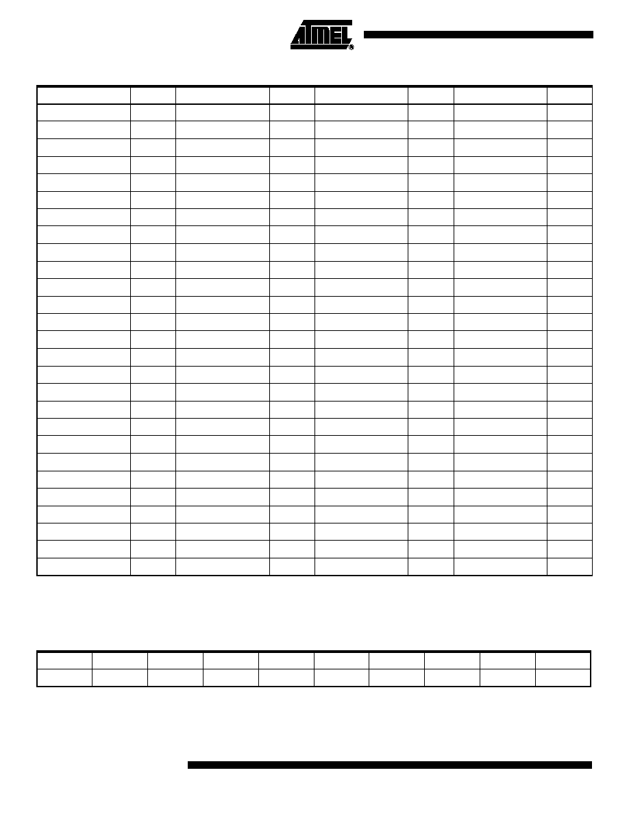
Table 3. D740 Ball Assignment (VDDI = 1.8V)
B18
B12
B6
T1
W3
AD6
AF11
AF19
AF23
W26
E23
Table 4. D740 Ball Assignment (VDDPLL = 1.8V)
P25
R26
Table 5.
D740 Ball Assignment (GND)
A1
C3
D23
W23
AD3
AF25
A2
C24
AC4
AD24
H4
AF26
A26
D4
AC8
J23
AE1
B2
D9
N4
AC13
AE2
B25
AE25
AC18
P23
D14
B26
AF1
AC23
D19
V4