 | –≠–ª–µ–∫—Ç—Ä–æ–Ω–Ω—ã–π –∫–æ–º–ø–æ–Ω–µ–Ω—Ç: SBN0064G | –°–∫–∞—á–∞—Ç—å:  PDF PDF  ZIP ZIP |

data sheet (v3)
2005 May 20
To improve design and/or performance,
Avant Electronics may make changes to its
products. Please contact Avant Electronics
for the latest versions of its products
DATA SHEET
SBN0064G
Dot-matrix STN LCD
64-SEGMENT Driver with
64-row x 64-column Display
Data Memory

2005 May 20
2 of 37
data sheet (v3)
Dot-matrix STN LCD 64-SEGMENT Driver with 64-row x 64-column Display Data Memory
SBN0064G
Avant Electronics
1
GENERAL
1.1
Description
The SBN0064G is a 64-SEGMENT driver with 64-row x64 column (4096-bit) on-chip Display Data Memory. It is designed
to be paired with the SBN6400G 64-COMMON driver to drive a STN LCD panel.
The on-chip Display Data Memory is for storing display data. Dot-matrix mapping method is used. A "0" stored in the
Display Data Memory bit corresponds to an OFF-pixel on the LCD panel; a "1" stored in the Display Data Memory bit
corresponds to an ON-pixel on the LCD panel.
Display on the LCD panel is controlled by a host microcontroller. The interface between the host microcontroller and the
SBN0064G is composed of 8-bit, bi-directional data bus (DB0~DB7) and control signals R/W, E, and C/D.
The SBN0064G does not have oscillator circuit. It depends on the SBN6400G to supply clocks (CLK1, CLK2) and display
control signals (CL, M, FRM).
1.2
Features
∑
64-SEGMENT STN LCD driver.
∑
To be paired with the SBN6400G 64-COMMON Driver.
∑
On-chip Display Data Memory: 64-row x 64-column (totally 4096 bits).
∑
Dot-Matrix Mapping between the Display Data Memory bit and LCD pixel.
∑
External LCD bias.
∑
Display duty cycle: 1/32 ~1/64.
∑
Normal mapping or Inverted mapping between SEGMENT outputs and Display Data Memory column outputs.
∑
Easy interface with a 8-bit host microcontroller.
∑
8-bit parallel data bus; READ/WRITE, Enable, and Command/Data control bus.
∑
Programmable internal registers: Display ON/OFF, Display Start Line, Page Address, Column Address, and Status.
∑
Display Data WRITE and display data READ.
∑
Operating voltage range (V
DD
): 2.7 ~ 5.5 volts.
∑
LCD bias voltage (V
LCD
=V
DD
- V5): 13 volts (max).
∑
Negative power supply (V
NEG
=V
DD
-V
EE
): 16 volts (max).
∑
Operating temperature range: -20 to +75
∞
C.
∑
Storage temperature range: -55 to +125
∞
C.

2005 May 20
3 of 37
data sheet (v3)
Dot-matrix STN LCD 64-SEGMENT Driver with 64-row x 64-column Display Data Memory
SBN0064G
Avant Electronics
1.3
Ordering information
Table 1 Ordering information
PRODUCT TYPE
DESCRIPTION
SBN0064G-LQFPG
LQFP100 Pb-free package.
SBN0064G-QFPG
QFP100 Pb-free package.
SBN0064G-LQFP
LQFP100 general package.
SBN0064G-QFP
QFP100 general package.
SBN0064G-D
tested die.

2005 May 20
4 of 37
data sheet (v3)
Dot-matrix STN LCD 64-SEGMENT Driver with 64-row x 64-column Display Data Memory
SBN0064G
Avant Electronics
2
FUNCTIONAL BLOCK DIAGRAM AND DESCRIPTION
2.1
Functional block diagram
V
EE2
V
EE1
Display Data RAM output latch
Fig.1 Functional Block Diagram
64 Output Drivers
64 row x 64column
(4096 bits)
Display Data Memory
Column Address Decoder
Li
ne
A
ddr
ess
Decoder
Display Data RAM Access Control
Display
Display Data
Read/Write
Control
Control
Mapping Circuit
Microcontroller
Interface
DB0
~
DB7
C
/D
E
R/W
Command
Decoder
RS
T
B
CLK1
CLK2
Display ON/OFF Register
Display Start Line Register
Page Address Register
Status Register
Column Address Register
M
V5L
V3L
V2L
SE
G
0
V0L
SE
G
1
SE
G6
2
SE
G6
3
FR
M
V5R
V3R
V2R
V0R
64 Level Shifters
High Voltage Circuit
Clock and display control
CL
CS1
B
CS2
B
CS3
CSM

2005 May 20
5 of 37
data sheet (v3)
Dot-matrix STN LCD 64-SEGMENT Driver with 64-row x 64-column Display Data Memory
SBN0064G
Avant Electronics
3
PIN(PAD) ASSIGNMENT, PAD COORDINATES, SIGNAL DESCRIPTION
3.1
The SBN0064G pinning diagram (LQFP100)
Fig.2 Pin assignment of LQFP100 package.
81
82
83
84
85
86
87
88
89
90
91
92
93
94
95
96
97
98
99
100
50
49
48
47
46
45
44
43
42
41
40
39
38
37
36
35
34
32
33
31
M
V
DD
V2R
V0R
SEG63
SEG62
SEG60
SEG59
SEG57
SEG54
SEG53
SEG52
SEG51
SEG50
V3R
V5R
V
EE2
SEG61
SEG58
SEG55
SEG56
SEG49
SEG48
SEG47
SEG46
SEG45
SEG44
SEG43
SEG42
CSM
DB
0
V
SS
V2L
V0L
SE
G
0
SEG1
SEG3
SEG4
SEG6
SEG9
SEG10
SEG11
SEG12
SE
G13
V3
L
V5L
V
EE1
SEG2
SEG5
SEG8
SEG7
SEG14
SEG15
SEG16
SEG17
SEG18
SEG19
SE
G20
SE
G
2
1
DB1
SEG22
SEG23
SEG24
SEG25
SEG26
SEG27
SEG28
SEG29
SEG30
SEG31
SEG32
SEG33
SEG34
SEG35
SEG36
SEG37
SEG38
SEG39
SEG40
SEG41
DB2
DB3
DB6
DB4
NC
CS3
CS2B
NC
DB7
DB5
NC
CS1B
RSTB
R/W
C/D
CL
CLK1
E
FRM
CLK2
SBN0064G
1 2 3 4 5 6 7 8 9 10 11 12 13 14 15 16 17 18 19 20 21 22 23 24 25 26 27 28 29 30
51
52
53
54
55
56
57
58
59
60
61
62
63
64
65
66
67
68
69
70
71
72
73
74
75
76
77
78
79
80

2005 May 20
6 of 37
data sheet (v3)
Dot-matrix STN LCD 64-SEGMENT Driver with 64-row x 64-column Display Data Memory
SBN0064G
Avant Electronics
3.2
The SBN0064G pad placement
V3R 4
81
82
83
84
85
86
87
88
89
90
91
92
93
94
95
96
97
1
2
V0R
V3L
V2L
30
31
32
33
34
35
36
37
38
39
40
41
42
43
SEG42
SEG41
SEG40
SEG39
SEG38
SEG37
SEG36
SEG35
SEG34
SEG33
SEG32
SEG31
SEG30
SEG29
SEG28
SEG27
SEG26
SEG25
SEG24
SEG23
45
46
47
48
44
49
29
28
27
26
25
24
23
22
21
20
18
17
16
15
14
13
12
11
10
9
8
7
19
SEG43
SEG44
SEG45
SEG46
SEG47
SEG48
SEG49
SEG51
SEG50
SEG52
SEG53
SEG54
SEG55
SEG57
SEG56
SEG58
SEG59
SEG60
SEG61
SEG62
SEG63
V
EE2
52
53
54
55
56
57
58
59
60
61
62
64
65
66
67
68
69
70
71
72
73
74
75
63
SEG20
SEG19
SEG18
SEG17
SEG16
SEG15
SEG14
SEG13
SEG12
SEG10
SEG11
SEG9
SEG8
SEG7
SEG6
SEG4
SEG5
SEG3
SEG2
SEG1
SEG0
V
EE1
V0L
V5L
76
77
(0,0) X
Y
Chip size : 3271
µ
m x 3120
µ
m.
Pad size: 90
µ
m x 90
µ
m.
5
V2R
V5R
6
ch
ip
ID
Fig.3 The pad placement
Note:
(1) The total pad number is 97.
(2) The chip ID is located at the lower left part of the chip.
(3) The chip ID of is 18005.
(4) The die origin is at the center of the chip.
(5) For chip_on_board bonding, chip carrier should be connected to VDD or
left open. Chip carrier is the metal pad to which the die is attached.
SEG22
SEG21
50
51
78
79
80
3271
µ
m
3120
µ
m
DB2
DB3
DB4
DB5
DB6
DB7
CS3
CS2B
CS1B
RSTB
R/W
C/D
CL
CLK2
CLK1
E
FRM
CSM
M
VDD
VSS
DB0
DB1
3
Pad 78

2005 May 20
7 of 37
data sheet (v3)
Dot-matrix STN LCD 64-SEGMENT Driver with 64-row x 64-column Display Data Memory
SBN0064G
Avant Electronics
3.3
Pad coordinates
Table 2 The pad coordinates (unit:
µ
m)
PAD
NO.
PAD
NAME
X
Y
PAD
NO.
PAD
NAME
X
Y
PAD
NO.
PAD
NAME
X
Y
1
CSM
-1506
-1066
35
SEG37
1512
-619
69
SEG3
-548
1434
2
M
-1506
-1181
36
SEG36
1512
-504
70
SEG2
-663
1434
3
VDD
-1512
-1300
37
SEG35
1512
-389
71
SEG1
-778
1434
4
V3R
-1512
-1430
38
SEG34
1512
-274
72
SEG0
-893
1434
5
V2R
-1338
-1434
39
SEG33
1512
-159
73
VEE1
-1008
1434
6
V5R
-1223
-1434
40
SEG32
1512
-44
74
V0L
-1124
1434
7
V0R
-1108
-1434
41
SEG31
1512
71
75
V5L
-1239
1434
8
VEE2
-993
-1434
42
SEG30
1512
186
76
V2L
-1355
1434
9
SEG63
-878
-1434
43
SEG29
1512
301
77
V3L
-1471
1434
10
SEG62
-763
-1434
44
SEG28
1512
416
78
VSS
-1471
1248
11
SEG61
-648
-1434
45
SEG27
1512
531
79
DB0
-1506
1119
12
SEG60
-533
-1434
46
SEG26
1512
646
80
DB1
-1506
1004
13
SEG59
-418
-1434
47
SEG25
1512
761
81
DB2
-1506
889
14
SEG58
-303
-1434
48
SEG24
1512
876
82
DB3
-1506
774
15
SEG57
-188
-1434
49
SEG23
1512
991
83
DB4
-1506
659
16
SEG56
-73
-1434
50
SEG22
1512
1106
84
DB5
-1506
544
17
SEG55
42
-1434
51
SEG21
1512
1221
85
DB6
-1506
429
18
SEG54
157
-1434
52
SEG20
1407
1434
86
DB7
-1506
314
19
SEG53
272
-1434
53
SEG19
1292
1434
87
CS3
-1506
199
20
SEG52
387
-1434
54
SEG18
1177
1434
88
CS2B
-1506
84
21
SEG51
502
-1434
55
SEG17
1062
1434
89
CS1B
-1506
-31
22
SEG50
617
-1434
56
SEG16
947
1434
90
RSTB
-1506
-146
23
SEG49
732
-1434
57
SEG15
832
1434
91
R/W
-1506
-261
24
SEG48
847
-1434
58
SEG14
716
1434
92
C/D
-1506
-376
25
SEG47
962
-1434
59
SEG13
602
1434
93
CL
-1506
-491
26
SEG46
1077
-1434
60
SEG12
486
1434
94
CLK2
-1506
-606
27
SEG45
1192
-1434
61
SEG11
372
1434
95
CLK1
-1506
-721
28
SEG44
1307
-1434
62
SEG10
257
1434
96
E
-1506
-836
29
SEG43
1422
-1434
63
SEG9
142
1434
97
FRM
-1506
-951
30
SEG42
1512
-1194
64
SEG8
27
1434
31
SEG41
1512
-1079
65
SEG7
-88
1434
32
SEG40
1512
-964
66
SEG6
-203
1434
33
SEG39
1512
-849
67
SEG5
-318
1434
34
SEG38
1512
-734
68
SEG4
-433
1434

2005 May 20
8 of 37
data sheet (v3)
Dot-matrix STN LCD 64-SEGMENT Driver with 64-row x 64-column Display Data Memory
SBN0064G
Avant Electronics
3.4
Signal description
Table 3 Pad signal description
To avoid a latch-up effect at power-on: V
SS
-
0.5 V < voltage at any pin at any time < V
DD
+ 0.5 V .
Pad
number
SYMBOL
I/O
DESCRIPTION
1
CSM
I
Column/Segment Mapping.
This signal controls the mapping relation between the column output of the Display
Data Memory and the SBN0064G's segment output.
If CMS=1, the mapping is called Normal Mapping. The mapping relation is that
Columns 0, 1, 2,...,62,63 of the Display Data Memory are mapped to Segments 0,
1, 2,..., 62, 63 of segment driver outputs.
If CMS=0, the mapping is called Inverted Mapping. The mapping relation is that
Columns 0, 1, 2,...,62,63 of the Display Data Memory are mapped to Segments 63,
62, 61,..., 2, 1, 0 of segment driver outputs.
2
M
Input
AC frame input.
The AC frame signal is the AC signal for generating alternating bias voltage of
reverse polarities for LCD cells.
This signal is supplied by the SBN6400G.
3
V
DD
Input
Power supply for logic part of the chip.
The V
DD
should be in the range from 2.7 volts to 5.5 volts.
4, 5, 6, 7
V3R, V2R,
V5R, V0R
Input
External LCD Bias voltage.
Note that V0R, V2R, V3R, and V5R must be connected to external bias voltages
V
DD
, V2, V3, and V5, respectively, and the condition V
DD
V1
V2
V3
V4
V5 must
always be met.
In addition, V
LCD
(V
DD
- V5) should not exceed 13 volts.
8
V
EE2
Input
Negative power supply for LCD bias.
This pad should be connected to the V
EE
of the external bias circuit.
9~72
SEG63~0
Output
SEGNENT driver outputs.
The output voltage level of SEGMENT outputs are decided by the combination of
the alternating frame signal (M) and display data. Depending on the value of the AC
frame signal and the display data, a single voltage level is selected from V0, V2,
V3, or V5 for SEGMENT driver, as shown in Fig. 4.
73
V
EE1
Input
Negative power supply for LCD bias.
This pad should be connected to the V
EE
of the external bias circuit.
0
1
0
1
0
1
0
1
0
1
0
1
0
V2
V5
V3
V0
V2
V5
V3
V0
Fig.4 SEGMENT driver output voltage level
M
Display
Data bit
SEG output

2005 May 20
9 of 37
data sheet (v3)
Dot-matrix STN LCD 64-SEGMENT Driver with 64-row x 64-column Display Data Memory
SBN0064G
Avant Electronics
74, 75,
76, 77
V3L, V2L,
V5L, V0L
Input
External LCD Bias voltage.
Note that V0L, V2L, V3L, and V5L must be connected to external bias voltages
V
DD
, V2, V3, and V5, respectively, and the condition VDD
V1
V2
V3
V4
V5 must
always be met.
In addition, V
LCD
(V
DD
- V5) should not exceed 13 volts.
78
V
SS
Ground.
79~86
DB0~DB7
I/O
Bi-direction, tri-state 8-bit parallel data bus for interface with a host microcontroller.
This data bus is for data transfer between the host microcontroller and the
SBN0064G.
87, 88,
89
CS3, CS2B,
CS1B
Input
Chip Selection
To enable selecting the SBN0064G as a peripheral device of the microcontroller,
the condition CS3=1, CS2B=0, and CS1B=0 must be met.
90
RSTB
Input
Hardware reset input.
A LOW pulse added to this input resets the internal circuit of the SBN0064G. The
duration of the low pulse must be longer than 1
µ
S.
91
R/W
Input
Read/Write (R/W) control signal from the host microcontroller.
This pin should be connected to the R/W output of the host microcontroller. A HIGH
level on this pin indicates that the microcontroller intends to do a READ operation.
A LOW level on this pin indicates that the microcontroller intends to do a WRITE
operation.
92
C/D
Input
COMMAND/DATA selection from the host microcontroller.
When C/D=0, the data on the 8-bit data bus (DB0~DB7) are either code data to be
written to an internal register, or status from the internal Status Register.
When C/D=1, the data on the 8-bit data bus (DB0~DB7) are data to be written to or
read from the Display Data Memory.
93
CL
Input
COMMON scan clock supplied by the SBN6400G.
The time duration of a COMMON output is equal to one clock period of CL.
94, 95
CLK1, CLK2 Inputs
Two-phase clocks for the control logic.
These two clocks are generated by the timing circuit of the SBN6400G COMMON
Driver.
96
E
Input
Enable signal (E) from the host microcontroller.
97
FRM
Input
Frame signal from the SBN6400G, indicating the start of a new frame.
Pad
number
SYMBOL
I/O
DESCRIPTION

2005 May 20
10 of 37
data sheet (v3)
Dot-matrix STN LCD 64-SEGMENT Driver with 64-row x 64-column Display Data Memory
SBN0064G
Avant Electronics
4
A SBN6400G AND SBN0064G-BASED DISPLAY SYSTEM
A SBN6400G and SBN0064G-based display system is shown in Fig. 5.
The SBN6400G contains timing generation circuit and 64 COMMON drivers. The timing generation circuit generates
operating clocks and display control signals (frame signal FRM , COMMON scan signal CL, and AC frame signal M), for
itself and the SBN0064G.
The SBN0064G contains 64 SEGMENT drivers, Display Data Memory, and interface circuit with a host microcontroller.
Host
Address bus
Data bus
Control bus
SBN0064G
SBN6400G
LCD Panel
SEG0
SEG1
SEG62
SEG63
COM0
COM1
COM62
COM63
Fig.5 A SBN6400G and SBN0064G-based display system
microcontroller
RESET
Decoder
Display Control
Signals
Display Data
Memory
Registers
LCD Bias Circuit
Microcontroller
Interface
Clock generation
circuit
clocks and
display control

2005 May 20
11 of 37
data sheet (v3)
Dot-matrix STN LCD 64-SEGMENT Driver with 64-row x 64-column Display Data Memory
SBN0064G
Avant Electronics
5
INTERFACE WITH A HOST MICROCONTROLLER
5.1
Interface signals and operation
The interface signals between the host microcontroller and the SBN0064G are data bus and control bus. The data bus
is an 8-bit (DB0~DB7) bi-directional bus. The control bus is composed of the following signals: C/D, E, and R/W.
By means of data bus and control bus, the host microcontroller can write data to or read data from the Display Data
Memory, can program the internal registers, and can read status of the SBN0064G. It is the host microcontroller's
responsibility to put proper data and timing on the data bus and control bus to ensure correct data transfer.
Fig. 6 gives an example for interface with an 8-bit microcontroller:
Fig. 7 gives an example for interface with a 68-family microcontroller
C/D
Address
D0~D7
E
R/W
RES
V
SS
V
DD
C/D
DB0~DB7
E
R/W
RSTB
V
DD
V
EE
V
SS
RESET
8-bit
Microcontroller
SBN0064G
V
DD
Negative
LCD bias voltage
Fig.6 Interface example with an 8-bit microcontroller
(indicating command/data)
Address or
I/O space
decoding
CS1B
CS2B
CS3
A0
A1~A15
VMA
D0~D7
E
R/W
RES
V
SS
VDD
C/D
DB0~DB7
E
R/W
RSTB
V
DD
V
EE
GND
RESET
DECODER
68-family
Microcontroller
SBN0064G
VDD
Negative
LCD bias voltage
Fig.7 Interface with a 68-family microcontroller
CS3
CS2B
CS1B

2005 May 20
12 of 37
data sheet (v3)
Dot-matrix STN LCD 64-SEGMENT Driver with 64-row x 64-column Display Data Memory
SBN0064G
Avant Electronics
Table 4 lists the setting for control bus and the types of data transfer.
Table 4 Interface signals and types of data transfer
5.2
Interface Timing (Writing to or reading from the SBN0064G)
Please refer to Fig. 16 and Fig. 17 for interface timing diagram and Table 25 and Table 26 for AC characteristics of
interface timing.
C/D
R/W
Types of data transfer
1
1
The host microcontroller reads data from the Display Data
Memory.
1
0
The host microcontroller writes data to the Display Data
Memory
0
1
The host microcontroller reads the Status Register.
0
0
The host microcontroller programs an internal register.

2005 May 20
13 of 37
data sheet (v3)
Dot-matrix STN LCD 64-SEGMENT Driver with 64-row x 64-column Display Data Memory
SBN0064G
Avant Electronics
6
DISPLAY DATA MEMORY AND LCD DISPLAY
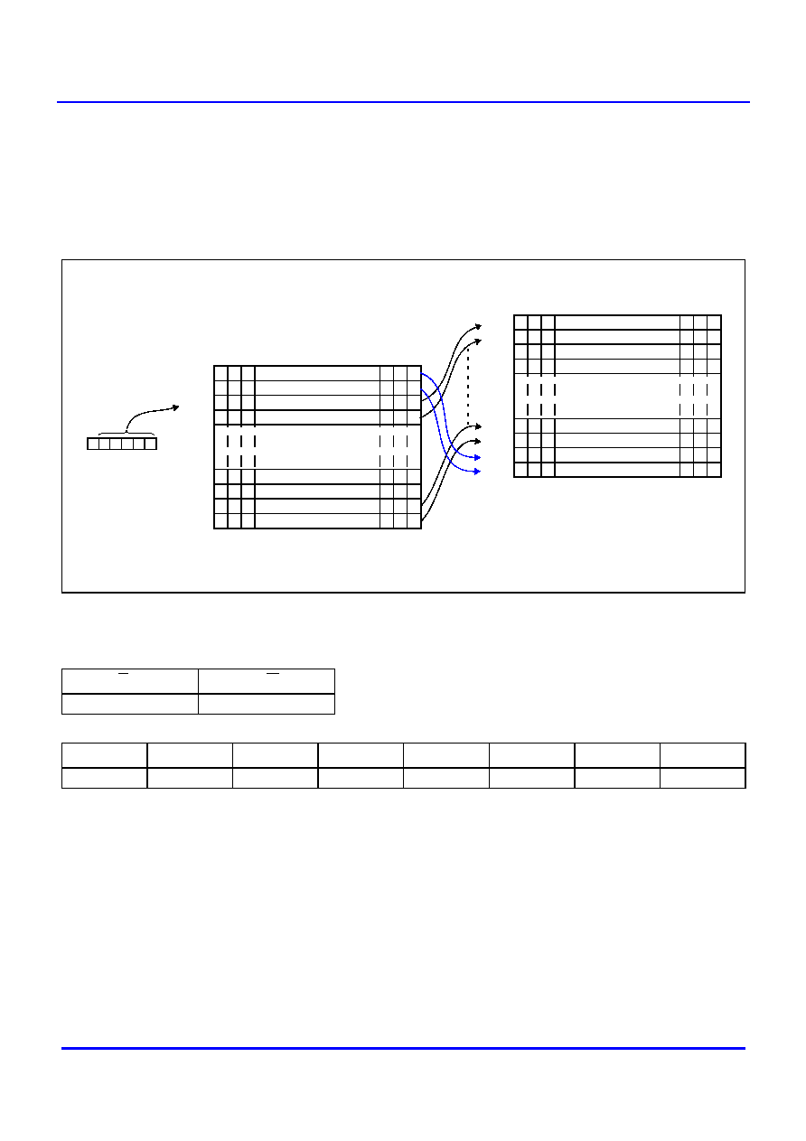
The Display Data Memory is a static memory bit(cell) array of 64-row x 64-column. So, the total bit number is
64 x 64 = 4096 bits (512 bytes). Each bit of the memory is mapped to a single pixel (dot) on the LCD panel. A "1" stored
in the Display Data Memory bit corresponds to an ON pixel (black dot in normal display). A "0" stored in the Display Data
Memory bit corresponds to an OFF pixel (background dot in normal display).
Column outputs (Column 0~63) of the Display Data Memory is mapped to SEG 0~63 outputs of the SBN0064G. The
mapping can be Normal Mapping or Inverse Mapping. Normal Mapping means that Column 0 is mapped to SEG0,
Column 1 to SEG1, Column 2 to SEG2, and so on. Inverse Mapping means that Column 0 is mapped to SEG 63, Column
1 to SEG 62, Column 2 to SEG 61, and so on. The mapping relation is decided by the CSM input (Column/Segment
Mapping). CSM=1 selects Normal Mapping and CSM=0 selects Inverse Mapping.
Any row (64 bits) of the Display Data Memory can be selected to map to the first row (COM0) of the LCD panel. This is
decided by the Display Start Line Register. The Display Start Line Register points at a row of the Display Data Memory,
which will be mapped to COM0 of LCD Display.
Fig.8 Memory cell array and LCD pixel array
Row 0
Row 1
Row 2
Row 3
Row 63
Row 62
Row 61
Row 60
Col
u
mn
0
Col
u
mn
1
Col
u
mn
2
Col
u
mn
6
3
Col
u
mn
6
2
Col
u
mn
6
1
COM 0
COM 1
COM 2
COM 3
COM 63
SEG
0
SEG
1
SEG
2
SEG
6
3
SEG
6
2
SEG
6
1
Display Data Memory Cell Array
LCD panel pixel array
Row 0
Row 1
Row 2
Row 3
Row 63
Row 62
Row 61
Row 60
Mapping between Column and SEG
is decided by the CSM input
Mapping between Row and COM
is decided by the Display Start Line
Register

2005 May 20
14 of 37
data sheet (v3)
Dot-matrix STN LCD 64-SEGMENT Driver with 64-row x 64-column Display Data Memory
SBN0064G
Avant Electronics
7
REGISTERS
7.1
Registers and their states after hardware RESET
The SBN0064G has 5 registers. Four of them must be programmed by the host microcontroller after hardware reset. The
Status Register can be read by the host microcontroller to check the current status of the SBN0064G.
The registers and their states after RESET is given in Table 5.
Table 5 Registers and their states after RESET
7.2
Display ON/OFF and the Display ON/OFF Register
The Display ON/OFF Register is a 1-bit Register. When this bit is programmed to HIGH, the display is turned ON. When
this bit is programmed to LOW, the display is turned OFF and SEG0 ~ SEG63 outputs are set to V
DD
.
To program this register, the setting of control bus is given in Table 6 and the setting of the data bus is given in Table 7.
Table 6 Setting of the control bus for programming the Display ON/OFF Register
Table 7 Setting of the data bus for programming the Display ON/OFF Register
When D0=1, the code is 3F(Hex) and the display is turned ON. When D0=0, the code is 3E(Hex) and the display is turned
OFF.
Register Name
Description
States after
RESET
Display ON/OFF Register
The Display ON/OFF Register is a 1-bit register. After RESET,
its value is LOW and, therefore, the LCD display is turned OFF.
0
Display Start Line Register
The Display Start Line Register is a 6-bit register. After RESET,
its value is 00 0000 and, therefore, Row 0 of the Display Data
Memory is mapped to COM0 of LCD panel.
00 0000
Page Address Register
The Page Address Register is a 3-bit register. It point to a page
of the Display Data Memory.
xxx
Column Address Register
The Column Address Register is a 6-bit register.
xx xxxx
Status Register
The Status Register shows the current state of the SBN0064G.
It is a 3-bit register, with each bit showing the status of a
programmed function.
0010 0000
C/D
R/W
0
0
D7(MSB)
D6
D5
D4
D3
D2
D1
D0(LSB)
0
0
1
1
1
1
1
D0
2005 May 20
15 of 37
data sheet (v3)
Dot-matrix STN LCD 64-SEGMENT Driver with 64-row x 64-column Display Data Memory
SBN0064G
Avant Electronics
7.3
Display Start Line and the Display Start Line Register
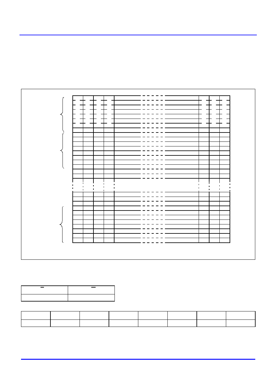
The Display Start Line Register is a 6-bit register. It points at the first row of a block of the Display Data Memory, which
will be mapped to COM0. The length of the block of the memory is decided by the display duty, which is decided by the
SBN6400G. For example, if the Display Start Line Register is programmed with 00010 (decimal 2) and display duty is
1/64, then Row2 of the Display Data Memory will be mapped to COM0 of LCD panel, Row3 to COM1, Row4 to COM2,
.....Row62 to COM60, Row63 to COM61, ....Row0 to COM62, and finally Row1 to COM63, as illustrated in Fig. 9.
To program this register, the setting of the control bus is given in Table 8 and the setting of the data bus is given in
Table 9.
Table 8 The setting of the control bus for programming the Display Start Line Register
Table 9 The setting of the data bus for programming the Display Start Line Register
A5 ~ A0 are Display Start Line address bits and can be programmed with a value in the range from 0 to 63. Therefore,
the code can be from 1100 0000 (C0 Hex) to 1111 1111 (FF Hex).
C/D
R/W
0
0
D7(MSB)
D6
D5
D4
D3
D2
D1
D0(LSB)
1
1
A5
A4
A3
A2
A1
A0
Fig.9 Display Start Line Register
Row 0
Row 1
Row 2
Row 3
Row 63
Row 62
Row 61
Row 60
Co
l
u
mn
0
Co
l
u
mn
1
Co
l
u
mn
2
Co
lumn
63
Co
lumn
62
Co
lumn
61
COM 0
COM 1
COM 2
COM 3
COM 63
COM 62
COM 61
COM 60
SE
G
0
SE
G
1
SE
G
2
SE
G
6
3
SE
G
6
2
SE
G
6
1
0
1
0
0
0
Display Start Line Register
A0
A1
A2
A3
A4
Display Data Memory
LCD panel
A5
0

2005 May 20
16 of 37
data sheet (v3)
Dot-matrix STN LCD 64-SEGMENT Driver with 64-row x 64-column Display Data Memory
SBN0064G
Avant Electronics
7.4
Mapping between Memory Columns and Segments
The mapping relation between the column outputs of the Display Data Memory and the Segment outputs SEG0~SEG63
is decided by the CSM (Column/Segment Mapping) input.
If CSM input is connected to HIGH, then data from column 0 of the Display Data Memory is output from SEG0. This type
of mapping is called normal mapping.
If CSM input is connected to LOW, then the data from column 63 of the Display Data Memory is output from SEG0. This
type of mapping is called inverted mapping.
By use of this input, the flexibility of component placement and routing on a PCB can be increased.
Fig.10 Column/Segment Mapping.
Row 0
Row 1
Row 2
Row 3
Row 63
Row 62
Row 61
Row 60
SE
G
0
SE
G
1
SE
G
2
SE
G
6
3
SE
G
6
2
SE
G
6
1
Display Data Memory
Segment Driver
Col
u
mn
0
Col
u
mn
1
Col
u
mn
2
Co
l
u
mn
61
Co
l
u
mn
62
Co
l
u
mn
63
Row 0
Row 1
Row 2
Row 3
Row 63
Row 62
Row 61
Row 60
SE
G
0
SE
G
1
SE
G
2
SE
G
6
3
SE
G
6
2
SE
G
6
1
Display Data Memory
Segment Driver
Col
u
mn
0
Col
u
mn
1
Col
u
mn
2
Co
l
u
mn
61
Co
l
u
mn
62
Co
l
u
mn
63
Inverted mapping
Normal Mapping
(CSM=0)
(CSM=1)
2005 May 20
17 of 37
data sheet (v3)
Dot-matrix STN LCD 64-SEGMENT Driver with 64-row x 64-column Display Data Memory
SBN0064G
Avant Electronics
7.5
Display Data Memory Page and the Page Address Register
The Display Data Memory is divided into 8 pages: Page 0 ~ Page 7, with each page having 64 bytes in horizontal
direction. Page 0 is from Row 0 to Row 7, Page 1 from Row 8 to Row 15, Page 2 from Row 16 to Row 23, and Page 3
from Row 24 to Row 31,...etc, as shown in Fig 11. When the host microcontroller intends to perform a READ/WRITE
operation to the Display Data Memory, it has to program the Page Address Register to indicate which page it intends to
access.
To program this register, the setting of the control bus is given in Table 10 and the setting of the data bus is given in Table
11.
Table 10 The setting of the control bus for programming the Page Address Register
Table 11 The setting of the data bus for programming the Page Address Register
A2, A1and A0 are page address bits and can be programmed with a value in the range from 0 to 7. A2 A1 A0=000 selects
Page 0; A2 A1 A0=001 selects Page 1; A2 A1 A0=010 selects Page 2, and A2 A1 A0=011 selects Page 3...etc.
Therefore, the code can be from 1011 1000 (B8 Hex) to 1011 1111 (BF Hex).
C/D
R/W
0
0
D7(MSB)
D6
D5
D4
D3
D2
D1
D0(LSB)
1
0
1
1
1
A2
A1
A0
Row 0
Row 1
Row 2
Row 3
Row 4
Row 5
Row 6
Row 7
Fig.11 Page/Column address of the Display Data Memory
Page 0
Page 1
Page 7
Row 8
Row 9
Row 10
Row 11
Row 12
Row 13
Row 14
Row 15
Row 16
Row 17
Row 18
Row19
Row52
Row 53
Row 54
Row 55
Row 56
Row 57
Row 58
Row 59
Row 60
Row 61
Row 62
Row 63
Bit0
Bit1
Bit2
Bit3
Bit4
Bit5
Bit6
Bit7
Bit0
Bit1
Bit2
Bit3
Bit4
Bit5
Bit6
Bit7
Bit0
Bit1
Bit2
Bit3
Bit4
Bit5
Bit6
Bit7
C
o
lu
mn
61(
Byte
61)
Col
u
mn
62
(Byte
62)
Col
u
mn
63
(Byte
63)
Col
u
mn
3(By
te3
)
Col
u
mn
2(By
te2
)
Col
u
mn
1(By
te1
)
Co
l
u
m
n
0
(
B
y
te
0)

2005 May 20
18 of 37
data sheet (v3)
Dot-matrix STN LCD 64-SEGMENT Driver with 64-row x 64-column Display Data Memory
SBN0064G
Avant Electronics
7.6
Column address and the Column Address Register
The Column Address Register points at a column of the Display Data Memory which the host microcontroller intends to
perform a READ/WRITE operation. To read or write a byte of the Display Data Memory, both its Page Address and
Column Address must be specified.
The Column Address Register automatically increments by 1 after a READ or WRITE operation is finished. When the
Column Address Register reaches 63, it overflows to 0. Please refer to Fig.11 for the column address sequence in a page
of the Display Data Memory.
To program this register, the setting of the control bus is given in Table 12 and the setting of the data bus is given in Table
13.
Table 12 The setting of the control bus for programming the Column Address Register
Table 13 The setting of the data bus for programming the Column Address Register
A5~A0 are column address bits and can be programmed with a value in the range from 0 to 63. Therefore, the code can
be from 0100 0000 (40 Hex) to 0111 1111 (7F Hex).
C/D
R/W
0
0
D7(MSB)
D6
D5
D4
D3
D2
D1
D0(LSB)
0
1
A5
A4
A3
A2
A1
A0
2005 May 20
19 of 37
data sheet (v3)
Dot-matrix STN LCD 64-SEGMENT Driver with 64-row x 64-column Display Data Memory
SBN0064G
Avant Electronics
7.7
Status Read and Status Register
The Status Register shows the current state of the SBN0064G. It can be read by the host microcontroller. Bits 4, 5, 7
shows the current status and Bits 0~3, and 6 are always fixed at 0.
To read the Status Register, the setting of the control bus is given in Table 14; the bit allocation is given in Table 15; the
description for each bit is given in Table 16.
Table 14 The setting of the control bus for reading the Status Register
Table 15 The Status Register bit allocation
Table 16 The Status Register bit description
C/D
R/W
0
1
D7(MSB)
D6
D5
D4
D3
D2
D1
D0(LSB)
BUSY
0
ON/OFF
RESET
0
0
0
0
Bit
Description
BUSY
BUSY=1 indicates that the SBN0064G is currently busy and can not accept new code or data. The
SBN0064G is executing an internal operation.
BUSY=0 indicates that the SBN0064G is not busy and is ready to accept new code or data.
ON/OFF
The ON/OFF bit indicates the current of status of display.
If ON/OFF=0, the display has been turned ON.
If ON/OFF=1, the display has been turned OFF.
Note that the polarity of this bit is inverse to that of the Display ON/OFF Register.
RESET
RESET=1 indicates that the SBN0064G is currently in the process of being reset.
RESET=0 indicates that the SBN0064G is currently in normal operation.

2005 May 20
20 of 37
data sheet (v3)
Dot-matrix STN LCD 64-SEGMENT Driver with 64-row x 64-column Display Data Memory
SBN0064G
Avant Electronics
8
READ OR WRITE OPERATION TO THE DISPLAY DATA MEMORY
READ or WRITE operation to the Display Data Memory is shown in Table 17. When performing a READ or WRITE
operation, the host microcontroller should give the control bus C/D, E, and R/W proper value and timing.
Table 17 READ/WRITE operation
8.1
Write Display Data
The Write Display Data operation writes a byte (8 bits) of data to the Display Data Memory. Data is put on the data bus
by the host microcontroller. The location which accepts this byte of data is pointed to by the Page Address Register and
the Column Address Register. At the end of the operation, the content of the Column Address Register is automatically
incremented by 1.
For page address and column address of the Display Data Memory, please refer to Fig. 11.
Table 18 gives the control bus setting for this command.
Table 18 The setting of the control bus for Write Display Data operation
Operation
DATA
Description
D7 D6 D5 D4 D3 D2 D1 D0
Write Display Data
Data to be written into the Display Data
Memory.
Write a byte of data to the Display Data Memory.
The data to be written is put on the data bus by the
host microcontroller.
Read Display Data
Data read from the Display Data
Memory output latch.
Read a byte of data from the Display Data Memory.
The data read from the internal 8-bit output latch
(refer to Fig. 12) appears on the data bus.
A dummy read is needed to get correct value.
C/D
R/W
1
0

2005 May 20
21 of 37
data sheet (v3)
Dot-matrix STN LCD 64-SEGMENT Driver with 64-row x 64-column Display Data Memory
SBN0064G
Avant Electronics
8.2
Read Display Data
The Read Display Data operation is a 3-step operation.
1. First, the current data of the internal 8-bit output latch of the Display Data Memory is read by the microcontroller, via
the 8-bit data bus DB0~DB7.
2. Then, a byte of data of the Display Data Memory is transferred to the 8-bit output latch from a location specified by
the Page Address Register and the Column Address Register,
3. Finally, the content of the Column Address Register is automatically incremented by one.
Fig. 12 shows the internal 8-bit output latch located between the 8-bit I/O data bus and the Display Data Memory cell
array. Because of this internal 8-bit output latch, a dummy read is needed to obtain correct data.
For Display Data Write operation, a dummy write is not needed, because data can be directly written from the data bus
to internal memory cells.
Table 19 gives the control bus setting for this command.
Table 19 The setting of the control bus for Read Display Data command
C/D
R/W
1
1
Fig.12 Read Display Data Memory
8-bit output latch
( 64 row x 64 column )
Display Data Memory cell array
Column Address Decoder
Row
A
d
d
re
ss
De
code
r
DB
0
DB
1
DB
2
DB
3
DB
4
DB
5
DB
6
DB
7
(8-bit bi-directional data bus)
Read Display Data
Write Display Data

2005 May 20
22 of 37
data sheet (v3)
Dot-matrix STN LCD 64-SEGMENT Driver with 64-row x 64-column Display Data Memory
SBN0064G
Avant Electronics
9
LCD BIAS CIRCUIT
A typical LCD bias circuit is shown Fig. 13. The condition V
DD
V1
V2
V3
V4
V5 must always be met. The
maximum allowed voltage for LCD bias (V
LCD
=V
DD
-V
5
) should not exceed 13 volts. Note that V0 should be connected to
V
DD
.
V0L/V0R
V2R/V2L
V3R/V3L
V5R/V5L
V
SS
V
DD
V0
V1
V2
V3
V4
V5
V
DD
V
DD
V
EE
SEG0~SEG63
C
C
C
C
C
Fig.13 LCD Bias circuit
C
OMPONENT
R
ECOMMENDED
V
ALUE
C
0.1
µ
F,
electrolytic
R1
2.2K
R2
10K
R3
10K
R1
R1
R1
R1
R2
R3
To SBN6400G
To SBN6400G
SBN0064G
V
EE1,
V
EE2
Note:
(1) V0 should always be connected to V
DD
.
(2) For cascading application, it is recommended that a
buffer be added for each of V1, V2, V3, V4, and V5.
For 64 COM x 64 SEG application, these buffers are
not needed.
(3) The LCD bias voltage (V
LCD
= V0 - V5) should not
exceed 13 volts, without regard to display duty.
(4) The voltage difference between V
DD
(the most
positive power) and V
EE
(the most negative
power), V
DD
- V
EE
, should not exceeds 16 volts,
without regards to display duty.

2005 May 20
23 of 37
data sheet (v3)
Dot-matrix STN LCD 64-SEGMENT Driver with 64-row x 64-column Display Data Memory
SBN0064G
Avant Electronics
10 COMMON, SEGMENT OUTPUT VOLTAGE
The output voltage level of COMMON driver (the SBN6400G) and SEGMENT driver (SBN0064G) is given in Table 20.
The output voltage level of COMMON driver is decided by the combination of AC Frame signal (M) and internal Shift
Register output.
The output voltage level of SEGMENT driver is decided by the combination of AC Frame signal (M), Display Data, and
the Display ON/OFF register.
Table 20 COMMON/SEGMENT output voltage level
Note that, in the above table, "Data" for the COM0~COM63 is actually the output of the internal Shift Register of the
SBN6400G COMMON driver, which sequentially activates COM0~COM63.
FR
Data
DISPLAY
ON/OFF
SEG0~SEG63
(SBN0064G)
COM0~COM63
(SBN6400G)
L
L
ON
V2
V1
L
H
ON
V0
V5
H
L
ON
V3
V4
H
H
ON
V5
V0
x(don't care)
x(don't care)
OFF
V2, V3
x
2005 May 20
24 of 37
data sheet (v3)
Dot-matrix STN LCD 64-SEGMENT Driver with 64-row x 64-column Display Data Memory
SBN0064G
Avant Electronics
11 MAXIMUM RATING
11.1
Absolute maximum rating
Table 21 Absolute maximum rating
Notes
1. The following applies to the Absolute Maximum Rating:
a) Stresses above those listed under Absolute Maximum Ratings may cause permanent damage to the device.
b) The SBN0064G includes circuitry specifically designed for the protection of its internal devices from the damaging
effect of excessive static charge (ESD). However, it is suggested that conventional precautions be taken to avoid
applying greater than the rated maxima.
c) Parameters are valid over operating temperature range unless otherwise specified.
d) All voltages are with respect to V
SS,
unless otherwise noted.
2. The condition V
DD
(V0)
V1
V2
V3
V4
V5 must always be met.
3. QFP-type packages are sensitive to moisture of the environment, please check the drypack indicator on the tray
package before soldering. Exposure to moisture longer than the rated drypack level may lead to cracking of the
plastic package or broken bonding wiring inside the chip.
SYMBOL
PARAMETER
MIN.
MAX.
UNIT
V
DD
voltage on the V
DD
pin(pad)
-
0.3
+7.0
volt
V
EE
voltage on the V
EE
pin(pad)
V
DD
- 16
V
LCD
(note 2)
LCD bias voltage, V
LCD
=V0-V5
13
V
I
input voltage on any pin with respect to V
SS
-
0.3
V
DD
+ 0.3
P
D
power dissipation
200
mW
T
stg
storage temperature range
-
55
+125
∞
C
T
amb
operating ambient temperature range
-30
+ 85
∞
C
Tsol (note 3)
soldering temperature/time at pin
260
∞
C,
10 Second

2005 May 20
25 of 37
data sheet (v3)
Dot-matrix STN LCD 64-SEGMENT Driver with 64-row x 64-column Display Data Memory
SBN0064G
Avant Electronics
12 DC CHARACTERISTICS
Table 22 DC Characteristics
V
DD
= 5 V
±
10%; V
SS
= 0 V; all voltages with respect to V
SS,
unless otherwise specified; T
amb
=
-2
0 to +75
∞
C.
Notes:
1. LCD bias voltage V
LCD
is V0 - V5. V0 should always be connected to VDD.
2. Conditions for the measurement: CLK1=CLK2=V
DD
, measured at the V
DD
pin.
3. This value is measured when the microcontroller does not perform any READ/WRITE operation to the chip and the
chip is only performing display operation, with the following condition: 1/64 duty, F
CLK1,CLK2
=250 KHz,
frame frequency= 70Hz, and no loading for SEG0~63.
4. This values is measured when the microcontroller continuously performs READ/WRITE operation to the chip and the
chip is also performing display operation with the following condition: 1/64 duty, F
CLK1,CLK2
=250 KHz,
frame frequency= 70Hz, and no loading for SEG0~63.
5. This measurement is for the transmission high-voltage PMOS or NMOS of SEG0~SEG63. Please refer to Section 16
for these driver circuit. The measurement is for the case when the voltage differential between the source and the
drain of the high voltage PMOS or NMOS is 0.1 volts.
SYMBOL
PARAMETER
CONDITIONS
MIN.
TYP.
MAX.
UNIT
V
DD
Supply voltage for logic
2.7
5.0
5.5
V
V
NEG
V
NEG
=V
DD
-V
EE
16
V
V
LCD
LCD bias voltage V
LCD
= V0(V
DD)
-V5 Note 1.
13
V
V
IL
LOW level input voltage
For all inputs
0
0.8
V
V
IH
HIGH level input voltage
For all inputs
V
DD
-2.2
V
DD
V
V
OL
LOW level output voltage of DB0~7
at I
OL
=1.6 mA.
0.0
0.3
V
V
OH
HIGH level output voltage of DB0~7
at I
OH
=-200
µ
A.
V
DD
- 0.3
V
DD
V
I
LKG
Leakage current of input pins
for all inputs
0.2
µ
A
I
STBY
Stand-by current at V
DD
=5 volts
Note 2
3.0
µ
A
I
DD(1)
Operating current for display-only
operation
Note 3
100
µ
A
I
DD(2)
Operating current for display and
microcontroller access at
t
CYC
=1 MHz
Note 4
500
µ
A
C
in
Input capacitance of all input pins
5.0
8.0
pF
R
ON
LCD driver ON resistance
Note 5
5.0
7.5

2005 May 20
26 of 37
data sheet (v3)
Dot-matrix STN LCD 64-SEGMENT Driver with 64-row x 64-column Display Data Memory
SBN0064G
Avant Electronics
13 AC TIMING CHARACTERISTICS
13.1
Display control signal (CL, FRM, and M) timing
Table 23 Display control signal (CL, FRM, and M) timing characteristics at V
DD
=5 volts
V
DD
= 5 V
±
10%; V
SS
= 0 V; all voltages with respect to V
SS
unless otherwise specified; T
amb
=
-2
0 to +75
∞
C.
SYMBOL
PARAMETER
CONDITIONS
MIN.
TYP.
MAX.
UNIT
T
WHCL
CL clock high pulse width
33
µ
s
T
WLCL
CL cock low pulse width
33
µ
s
T
R
CL clock rise time
28
120
ns
T
F
CL clock fall time
28
120
ns
T
DF
FR delay time (input)
-1.8
1.8
µ
S
T
DM
FR delay time (output)
-1.8
1.8
µ
S
Fig.14 Display Control Signal Timgin
T
WLCL
T
WHCL
T
R
T
F
T
DM
CL
M
0.8 x V
DD
0.2 x V
DD
0.2 x V
DD
0.2 x V
DD
0.2 x V
DD
0.2 x V
DD
0.8 x V
DD
0.8 x V
DD
FRM
0.8 x V
DD
T
DF
0.2 x V
DD
T
DF
0.8 x V
DD

2005 May 20
27 of 37
data sheet (v3)
Dot-matrix STN LCD 64-SEGMENT Driver with 64-row x 64-column Display Data Memory
SBN0064G
Avant Electronics
13.2
CLK1, CLK2 timing
Table 24 CLK1 and CLK2 timing characteristics
V
DD
= 5 V
±
10%; V
SS
= 0 V; all voltages with respect to V
SS
unless otherwise specified; T
amb
=
-2
0 to +75
∞
C.
SYMBOL
PARAMETER
CONDITIONS
MIN.
TYP.
MAX.
UNIT
T
WH1
CLK1 clock high pulse width
2000
ns
T
WL1
CLK1 cock low pulse width
600
T
R1
CLK1 clock rise time
130
T
F1
CLK1 clock fall time
130
T
WH2
CLK2 clock high pulse width
2000
T
WL2
CLK2 clock low pulse width
600
T
R2
CLK2 clock rise time
130
T
F2
CLK2 clock fall time
130
T
D12
CLK1-to-CLK2 delay
660
T
D21
CLK2-to-CLK1 delay
660
Fig.15 CLK1, CLK2 Timing
0.8VDD
0.2VDD
0.8VDD
0.8VDD
0.8VDD
0.8VDD
0.2VDD
0.2VDD
0.2VDD
0.8VDD
CLK1
CLK2
t
WH1
t
WH2
t
WL2
t
WL1
t
D12
t
D21
t
F1
t
F2
t
R1
t
R2

2005 May 20
28 of 37
data sheet (v3)
Dot-matrix STN LCD 64-SEGMENT Driver with 64-row x 64-column Display Data Memory
SBN0064G
Avant Electronics
13.3
Microcontroller interface timing for writing to the SBN0064G
Table 25 AC timing for writing to the SBN0064G
V
DD
= 5 V
±
10%; V
SS
= 0 V; T
amb
= -20
∞
C to +75
∞
C.
symbol
parameter
min.
max.
test conditions
unit
t
CYC
Enable (E) cycle time
1000
ns
t
EWL
Enable (E) LOW width
450
t
EWH
Enable (E) HIGH width
450
t
R
Enable (R) rise time
20
t
F
Enable (F) fall time
20
t
AS1
Write set-up time
140
t
AH1
Write hold time
10
t
AS2
C/D, CS1B, CS2B, CS3 set-up time
140
t
AH2
C/D, CS1B, CS2B, CS3 hold time
10
t
DSW
Data setup time (on the data bus)
200
The loading on
the data bus is
shown in Fig. 18.
t
DHW
Data hold time (on the data bus)
10
Fig.16 AC timing for writing to the SBN0064G
R/W
D0 to D7
t
DSW
t
DHW
(Data on the data bus)
0.8 x VDD
0.2 x VDD
0.2 x VDD
0.2 x VDD
0.2 x VDD
0.8 x VDD
C/D, CS1B
0.2 x VDD
0.2 x VDD
0.8 x VDD
0.8 x VDD
E
0.2 x VDD
0.2 x VDD
0.8 x VDD
t
AS1
t
AS2
t
AH1
t
AH2
0.8 x VDD
0.2 x VDD
t
R
t
F
t
EWH
CS2B, CS3
t
CYC
t
EWL

2005 May 20
29 of 37
data sheet (v3)
Dot-matrix STN LCD 64-SEGMENT Driver with 64-row x 64-column Display Data Memory
SBN0064G
Avant Electronics
13.4
Microcontroller interface timing for reading from the SBN0064G
Table 26 AC timing for reading from the SBN0064G
V
DD
= 5 V
±
10%; V
SS
= 0 V; T
amb
= -20
∞
C to +75
∞
C.
symbol
parameter
min.
max.
test conditions
unit
t
CYC
Enable (E) cycle time
1000
ns
t
EWL
Enable (E) LOW width
450
t
EWH
Enable (E) HIGH width
450
t
R
Enable (R) rise time
20
t
F
Enable (F) fall time
20
t
AS1
READ set-up time
140
t
AH1
READ hold time
20
t
AS2
C/D, CS1B, CS2B, CS3 set-up time
140
t
AH2
C/D, CS1B, CS2B, CS3 hold time
10
t
DDR
Data delay time (on the data bus)
320
The loading on
the data bus is
shown in Fig. 18.
t
DHR
Data hold time (on the data bus)
20
Fig.17 AC timing for reading from the SBN0064G
R/W
D0 to D7
t
DDR
t
DHR
(Data on the data bus)
0.8 x VDD
0.2 x VDD
0.2 x VDD
0.8 x VDD
0.8 x VDD
0.8 x VDD
C/D, CS1B
0.2 x VDD
0.2 x VDD
0.8 x VDD
0.8 x VDD
E
0.2 x VDD
0.2 x VDD
0.8 x VDD
t
AS1
t
AS2
t
AH1
t
AH2
0.8 x VDD
0.2 x VDD
t
R
t
F
t
EWH
CS2B, CS3
t
CYC
t
EWL
Fig.18 Load circuit for each bit of the data bus.
V
SS
C
L
C
L
= 50 pF (including wiring and probe capacitance).
Pin

2005 May 20
30 of 37
data sheet (v3)
Dot-matrix STN LCD 64-SEGMENT Driver with 64-row x 64-column Display Data Memory
SBN0064G
Avant Electronics
14 APPLICATION EXAMPLE (1/64 DISPLAY DUTY)
14.1
Application circuit for 1/64 display duty
Fig.19 Application circuit for 1/64 display duty
M
CL
FRM
CLK1
CLK2
M
CL
FRM
CLK1
CLK2
SEG0
SEG63
COM0
COM63
COM0
COM63
SEG0
SEG63
SHL
DS1
DS2
FS
M/S
PSEL
DIO1
DIO2
V
DD
V
SS
V
DD
open
open
V0L, V0R
V1L, V1R
V4L, V4R
V5L, V5R
LCD Bias Circuit
V0, V1, V2, V3, V4, V5
V
DD
V
DD
V
SS
V
EE
V
EE
V
EE
V0, V2, V3, V5
SBN0064G
SBN6400G
64 COM x 64 SEG
LCD panel
V
DD
V
SS
V
DD
R
f
33K
C
f
20P
C
CR
R
R/
W
E
C
/D
CS
1B
CS
2B
CS
3
DB
0
~
DB7
RS
TB
Decoder
R/W
E
C
/D
Addre
ss Bu
s
DB
0
~
D
B
7
RS
T
B
Host Microcontroller

2005 May 20
31 of 37
data sheet (v3)
Dot-matrix STN LCD 64-SEGMENT Driver with 64-row x 64-column Display Data Memory
SBN0064G
Avant Electronics
14.2
Timing Diagram of 1/64 display duty
63
0
1
2
63
0
1
2
63
0
CL
FRM
M
COM63
COM0
SEG0
SEG63
COM1
One Frame
One Frame
V3
V3
V0
V0
V2
V2
V5
V5
V0
V0
V3
V3
V4
V4
V4
V0
V5
V1
V1
V1
V5
V1
V5
V0
V4
V4
V5
V1
V4
V0
V4
V0
V1
Fig.20 Timing diagram for 1/64 display duty
Note:
COMMON is the scan signal for horizontal display line.
SEGMENT is the display data from the on-chip display data. The
wave form of this example shows that only the top line of the
panel is turned ON.
COMMO
N
SEGMEN
T
0
1
2
3
4
92
93
94
95
91
Note:
(1) CLK is the clock from the
RC-oscillator.
(2) The frequency of both CLK1 and
CLK2 is a half of the CLK.
T
CL
CLK
CLK1
CLK2
0
1
47
46
T
CL

2005 May 20
32 of 37
data sheet (v3)
Dot-matrix STN LCD 64-SEGMENT Driver with 64-row x 64-column Display Data Memory
SBN0064G
Avant Electronics
15 MASTER/SLAVE APPLICATION EXAMPLE
Fig.21 Master/Slave application example
COM64
COM127
SEG0
SEG63
SBN6400G
SBN0064G
M, CL, FRM,
CLK1, CLK2
COM0
COM63
SBN0064G
SEG63
SEG0
128 x 192 LCD Panel
SBN6400G
M, CL
Master
Slave
SBN0064G
SBN0064G
SEG64
SEG12
7
SBN0064G
SEG12
8
SEG19
1
SBN0064G
SEG61
27
SEG64
SEG19
1
SEG12
8
R
f
33K
C
f
20P

2005 May 20
33 of 37
data sheet (v3)
Dot-matrix STN LCD 64-SEGMENT Driver with 64-row x 64-column Display Data Memory
SBN0064G
Avant Electronics
16 PIN CIRCUITS
Table 27 MOS-level schematics of all input, output, and I/O pins.
SYMBOL
Input/output
CIRCUIT
NOTES
C/D, R/W, E,
CS1B,
CS2B, CS3,
RSTB
Inputs
CLK1,
CLK2, FRM,
CL, M, CSM
Input
DB0~DB7
I/O
SEG0~63
VSS
VDD
VSS
VDD
VSS
VDD
VSS
VDD
VSS
VDD
Data out
Output Enable
Data in
Enable
VSS
VDD
V0R, V0L
V2R, V2L
V3R, V3L
V5R, V5L
V
EE
VDD
EN1
EN2
EN3
EN4
VDD
VDD
VDD
V
EE
V
EE
V
EE
SEG0~63
VDD
V
EE

2005 May 20
34 of 37
data sheet (v3)
Dot-matrix STN LCD 64-SEGMENT Driver with 64-row x 64-column Display Data Memory
SBN0064G
Avant Electronics
17 APPLICATION NOTES
1. It is recommended that the following power-up sequence be followed to ensure reliable operation of your display
system. As the ICs are fabricated in CMOS and there is intrinsic latch-up problem associated with any CMOS
devices, proper power-up sequence can reduce the danger of triggering latch-up. When powering up the system,
control logic power must be powered on first. When powering down the system, control logic must be shut off later
than or at the same time with the LCD bias (V
EE
).
2. The metal frame of the LCD panel should be grounded.
3. A 0.1
µ
F ceramic capacitor should be connected between V
DD
and V
SS
.
4. A 0.1
µ
F ceramic capacitor should be connected between V
DD
(or V
SS
) and each of V1, V2, V3, V4, and V5.
5. If the length of the cable connecting the host microcontroller and the LCD module is longer than 45 cm, a ceramic
capacitor of 20P~150P should be connected between V
DD
(or V
SS
) and each of the R/W, E, and C/D.
VDD
Signal
VEE
5V
0V
-11V
0~50 ms
1 second (minimum)
0 second
0 second
(minimum)
(minimum)
0~50 ms
1 second (minimum)
Fig.22 Recommended power up/down sequence

2005 May 20
35 of 37
data sheet (v3)
Dot-matrix STN LCD 64-SEGMENT Driver with 64-row x 64-column Display Data Memory
SBN0064G
Avant Electronics
18 PACKAGE INFORMATION
Package information is provided in another
document. Please contact Avant Electronics for
package information.

2005 May 20
36 of 37
data sheet (v3)
Dot-matrix STN LCD 64-SEGMENT Driver with 64-row x 64-column Display Data Memory
SBN0064G
Avant Electronics
19 SOLDERING
19.1
Introduction
There is no soldering method that is ideal for all IC packages. Wave soldering is often preferred when through-hole and
surface mounted components are mixed on one printed-circuit board. However, wave soldering is not always suitable for
surface mounted ICs, or for printed-circuits with high population densities. In these situations reflow soldering is often
used.
This text gives a very brief insight to a complex technology. For more in-depth account of soldering ICs, please refer to
dedicated reference materials.
19.2
Reflow soldering
Reflow soldering techniques are suitable for all QFP packages.
The choice of heating method may be influenced by larger plastic QFP packages (44 leads, or more). If infrared or vapour
phase heating is used and the large packages are not absolutely dry (less than 0.1% moisture content by weight),
vaporization of the small amount of moisture in them can cause cracking of the plastic body. For more information, please
contact Avant for drypack information.
Reflow soldering requires solder paste (a suspension of fine solder particles, flux and binding agent) to be applied to the
printed-circuit board by screen printing, stencilling or pressure-syringe dispensing before package placement.
Several techniques exist for reflowing; for example, thermal conduction by heated belt. Dwell times vary between
50 and 300 seconds depending on heating method. Typical reflow temperatures range from 215 to 250
∞
C.
Preheating is necessary to dry the paste and evaporate the binding agent. Preheating duration: 45 minutes at 45
∞
C.
19.3
Wave soldering
Wave soldering is not recommended for QFP packages. This is because of the likelihood of solder bridging due to
closely-spaced leads and the possibility of incomplete solder penetration in multi-lead devices.
If wave soldering cannot be avoided, the following conditions must be observed:
∑
A double-wave (a turbulent wave with high upward pressure followed by a smooth laminar wave) soldering
technique should be used.
∑
The footprint must be at an angle of 45
∞
to the board direction and must incorporate solder thieves
downstream and at the side corners.
During placement and before soldering, the package must be fixed with a droplet of adhesive. The adhesive can be
applied by screen printing, pin transfer or syringe dispensing. The package can be soldered after the adhesive is cured.
Maximum permissible solder temperature is 260
∞
C, and maximum duration of package immersion in solder is
10 seconds, if cooled to less than 150
∞
C within 6 seconds. Typical dwell time is 4 seconds at 250
∞
C.
A mildly-activated flux will eliminate the need for removal of corrosive residues in most applications.
19.4
Repairing soldered joints
Fix the component by first soldering two diagonally- opposite end leads. Use only a low voltage soldering iron (less
than 24 V) applied to the flat part of the lead. Contact time must be limited to 10 seconds at up to 300
∞
C. When using a
dedicated tool, all other leads can be soldered in one operation within 2 to 5 seconds between 270 and 320
∞
C.

2005 May 20
37 of 37
data sheet (v3)
Dot-matrix STN LCD 64-SEGMENT Driver with 64-row x 64-column Display Data Memory
SBN0064G
Avant Electronics
20 LIFE SUPPORT APPLICATIONS
Avant's products, unless specifically specified, are not designed for use in life support appliances, devices, or systems
where malfunction of these products can reasonably be expected to result in personal injury. Avant customers using or
selling Avant's products for use in such applications do so at their own risk and agree to fully indemnify Avant for any
damages resulting from such improper use or sale.