 | –≠–ª–µ–∫—Ç—Ä–æ–Ω–Ω—ã–π –∫–æ–º–ø–æ–Ω–µ–Ω—Ç: aTS50 | –°–∫–∞—á–∞—Ç—å:  PDF PDF  ZIP ZIP |
New Release Specification
© Andigilog, Inc. 2003
www.andigilog.com
70A03202-001
L
OW
-V
OLTAGE
SOT-23 T
EMPERATURE
S
ENSOR
aTS50
P
RODUCT
S
PECIFICATION
General Description
The aTS50 is a high-precision CMOS temperature
sensor that provides a cost-effective solution for
applications requiring high-accuracy low-power
temperature monitoring. The aTS50 output voltage
ramp is extremely linear and has a slope of 10mV/∞C.
With a supply voltage of 2.7V to 6V, the aTS50 is
accurate to ±1∞C over a temperature range of
-
40∞C to
125∞C and has a typical room temperature accuracy of
±0.5∞C. Reducing the supply voltage to 2.7V does not
change the negative and positive temperature
extremes. As well, the aTS50 does not require
external calibration. Calibration of each device is
performed at the factory.
Features
∑
= Precision Calibrated to ±1∞C at 25∞C
∑
= Temperature Range: -40∞C to 125∞C
∑
= Extremely Linear Output Ramp: 10mV/∞C
∑
= Output Ramp is Calibrated to Degrees Celsius
∑
= Low Operating Current:
130
µ
A
∑
= Low Self Heating: 0.2∞C Typical in Still Air
∑
= Operating Voltage Range: +2.7V to +6V
∑
= Uses a Single Positive Supply
∑
= Non-linearity:
0.8
∞
C
Applications
∑
= Mobile Phones
∑
= Mobile Communications Terminals
∑
= Computers
∑
= Battery Management
∑
= FAX Machines/Printers/Copiers
∑
= Portable Medical Instruments
∑
= HVAC
∑
= Power Supply Modules
∑
= Disk Drives
∑
= Automotive Control Circuits
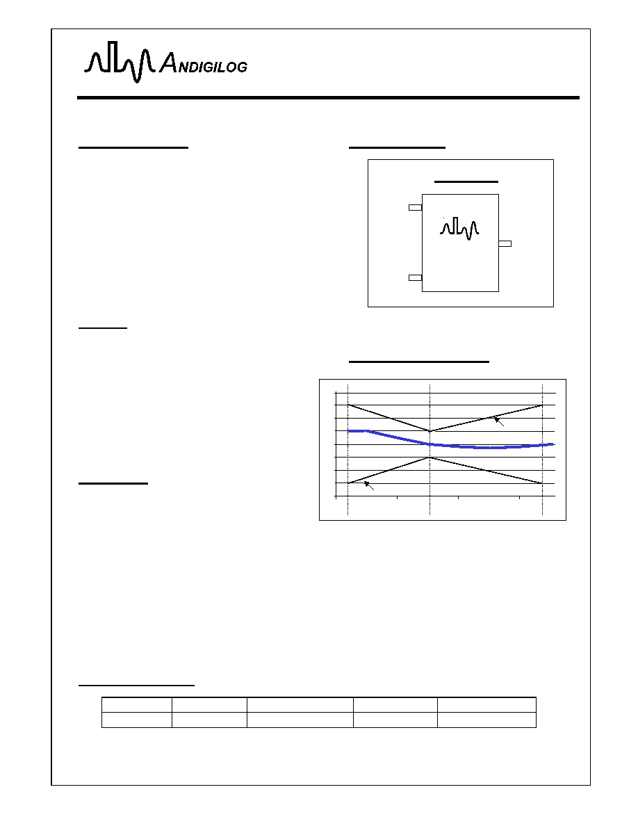
Pin Configuration
2
1
3
SOT- 23 3-lead
GND
V
OUT
V
DD
2
1
3
SOT- 23 3-lead
GND
V
OUT
V
DD
aTS50
2
1
3
SOT- 23 3-lead
GND
V
OUT
V
DD
2
1
3
SOT- 23 3-lead
GND
V
OUT
V
DD
aTS50
actual part marking below
Accuracy vs Temperature
Ordering Information
Part Number
Package
Temperature Range
Part Marking
How Supplied
aTS50S3 3-Pin
SOT-23 -40∞C to +125∞C
AAyw
3000 units on T&R
y ≠ year, w - week
-50
0
50
100
Temperature (∞C)
A
ccura
cy
(∞C
)
V
DD
=+5V
lower spec limit
-4
-3
-2
-1
0
1
2
3
upper spec limit
-40
25
125
4
-50
0
50
100
Temperature (∞C)
A
ccura
cy
(∞C
)
V
DD
=+5V
lower spec limit
-4
-3
-2
-1
0
1
2
3
upper spec limit
-40
25
125
4
-
2
-
© Andigilog, Inc. 2003
www.andigilog.com
70A03202-001
aTS50
Absolute Maximum Ratings
1
Notes:
1. Absolute maximum ratings are limits beyond
which operation may cause permanent damage to
the device. These are stress ratings only;
functional operation at or above these limits is not
implied.
2. Human Body Model: 100pF capacitor discharged
through a 1.5k
resistor into each pin. Machine
Model: 200pF capacitor discharged directly into
each pin.
3. These specifications are guaranteed only for the
test conditions listed.
Recommended Operating Ratings
Symbol Parameter Min
Max
Units
V
DD
Supply
Voltage
+2.7
+6
V
V
OUT
Output
Voltage
0
V
DD
V
T
A
Operating Temperature Range
-40
+125
∞C
Electrical Characteristics
3
Limits apply for -40∞C
T
A
+125∞C and V
D D
= + 5.0V unless otherwise noted.
Parameter Symbol
Conditions
Min
Typ
Max
Units
Accuracy
4
T
A
=+25∞C
T
A
=-40∞C
(T
MIN
)
T
A
=+125∞C (T
MAX
)
-1
-3
-3
±0.5
±1
±1
+1
+3
+3
∞C
∞C
∞C
Non-linearity
5
±0.8
∞C
Supply Current ≠ Output floating
I
DD
T
A
=+25∞C
130
µ
A
Output Sink Capability
6
I
OL
+2.7V < V
DD
< +6V
50
µ
A
Output Source Capability
6
I
OH
+2.7V < V
DD
< +6V
25
µ
A
Average Output Slope
(Sensor Gain)
A
OUT
10
mV/∞C
Room Temperature Output
Voltage
V
OUT25
T
A
=+25∞C
750
mV
Self Heating
7
SOT-23
0.21840
∞C
Notes:
4. Accuracy (expressed in ∞C) = Difference between calculated output voltage and measured output voltage.
Calculated output voltage = 10mV/∞C multiplied by device's case temperature at specified conditions of
temperature, voltage and power supply.
5. Non-linearity is defined as the deviation of the output-voltage-versus-temperature curve from the best-fit straight
line, over the device's rated temperature range.
6. Lowest output current should be targeted; higher currents result in more self-heating of the device.
7. Max Self Heating =
JA
x (V
DD
x I
DD
). Assumes a capacitive load.
Parameter Rating
Supply Voltage
+7V
Output Voltage
V
DD
+ 0.5V
Output Current
-50/+25 µA
Storage Temperature Range
-60∞C to +150∞C
Human Body Model
2000V
ESD
2
Machine Model
250V
Thermal Resistance -
JA
336∞C/W
Vapor Phase (60 sec)
215∞C
Lead
Temp Infrared (15 sec)
220∞C

-
3
-
© Andigilog, Inc. 2003
www.andigilog.com
70A03202-001
aTS50
Figure 1. aTS50 Output Voltage vs. Temperature
Mounting
The aTS50 can be easily mounted by gluing or
cementing it to a surface. In this case, its temperature
will be within about 0.2∞C of the temperature of the
surface it is attached to if the ambient air temperature
is almost the same as the surface temperature. If the
air temperature is much higher or lower than the
surface temperature, the actual temperature of the
aTS50 die will be at an intermediate temperature
between the surface temperature and the air
temperature.
To ensure good thermal conductivity, the backside of
the aTS50 die is directly attached to the GND pin. The
lands and traces to the aTS50 will, of course, be part of
the printed circuit board, which is the object whose
temperature is being measured. These printed circuit
board lands and traces will not cause the aTS50's
temperature to deviate from the desired temperature.
Alternatively, the aTS50 can be mounted inside a
sealed-end metal tube, and can then be dipped into a
bath or screwed into a threaded hole in a tank. As
with any IC, the aTS50 and accompanying wiring and
circuits must be kept insulated and dry to avoid
leakage and corrosion. This is especially true if the
circuit may operate at cold temperatures where
condensation can occur. Printed-circuit coatings and
varnishes such as Humiseal and epoxy paint or dips
can be used to ensure that moisture cannot corrode
the aTS50 or its connections.
25
50
75
100
125
-25
-50 -40
0
1750
100
750
500
V
OUT
(mV)
Temperature (∫C)
1500
Temp (∫C) = (V
OUT
≠ 500mV) / 10mV/∫C
25
50
75
100
125
-25
-50 -40
0
1750
100
750
500
V
OUT
(mV)
Temperature (∫C)
1500
25
50
75
100
125
-25
-50 -40
0
25
50
75
100
125
-25
-50 -40
0
1750
100
750
500
V
OUT
(mV)
Temperature (∫C)
1500
Temp (∫C) = (V
OUT
≠ 500mV) / 10mV/∫C

- 4 -
© Andigilog, Inc. 2003
www.andigilog.com
70A03202-001
aTS50
Typical Performance Characteristics
-50
0
50
100
Temperature (∞C)
A
c
cu
r
a
cy
(
∞
C
)
V
DD
=+5V
lower spec limit
-4
-3
-2
-1
0
1
2
3
upper spec limit
-40
25
125
4
-50
0
50
100
Temperature (∞C)
A
c
cu
r
a
cy
(
∞
C
)
V
DD
=+5V
lower spec limit
-4
-3
-2
-1
0
1
2
3
upper spec limit
-40
25
125
4
Figure 2. aTS50 Accuracy Range vs Temperature
I
DD
(
mA
)
90
110
120
130
-50
-25
0
25
50
75
100
125
-50
-25
0
25
50
75
100
125
Temperature (∞C)
V
DD
= +5V
60
70
80
50
40
30
20
10
0
100
I
DD
(
mA
)
90
110
120
130
-50
-25
0
25
50
75
100
125
-50
-25
0
25
50
75
100
125
Temperature (∞C)
V
DD
= +5V
60
70
80
50
40
30
20
10
0
100
Figure 3. aTS50 Current vs Temperature
- 5 -
© Andigilog, Inc. 2003
www.andigilog.com
70A03202-001
aTS50
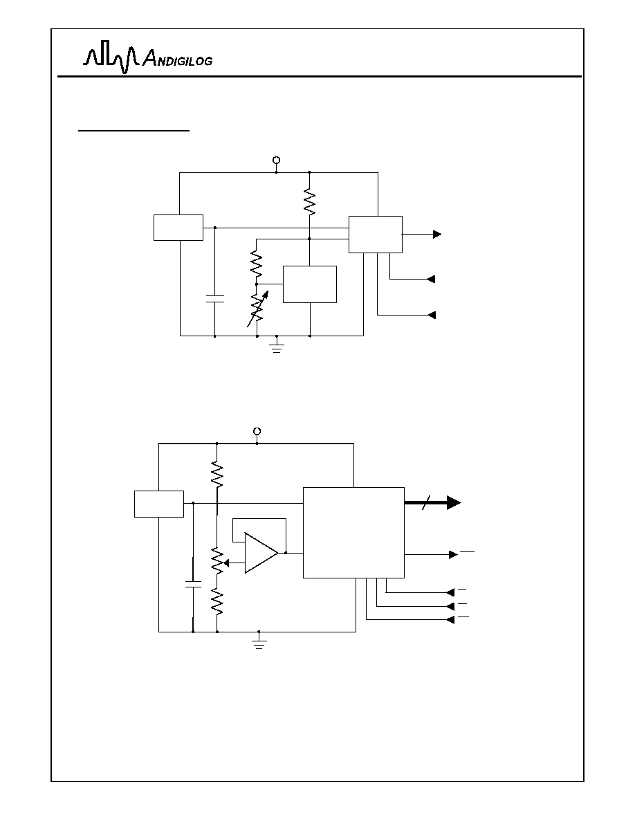
Typical Applications
Figure 4. Serial Output Temperature to Digital Converter (Full Scale = +125∞C)
Figure 5. Parallel Output Temperature to Digital Converter (Full Scale = +125∞C)
IN
10K
100K
1
µ
F
FB
1.75V
REF
3.9K
SERIAL
DATA OUT
CLOCK
ENABLE
aTS50
5V
V
Temp
U1
U2
U3
Serial
Analog-to-Digital
Converter
Adjustable
Shunt Voltage
Reference
+
5V
WR
5K
30K
IN
V
REF
1.75V
15K
1
µ
F
+
_
PARALLEL
DATA
OUTPUT
INTR
CS
RD
8
V
Temp
Parallel Output
Analog-to-Digital
Converter
aTS50
U1
U3
U2