 | –≠–ª–µ–∫—Ç—Ä–æ–Ω–Ω—ã–π –∫–æ–º–ø–æ–Ω–µ–Ω—Ç: MSC1210SS | –°–∫–∞—á–∞—Ç—å:  PDF PDF  ZIP ZIP |

1/11
MSC1210
° Semiconductor
FEDL1210-03
GENERAL DESCRIPTION
The MSC1210 is a clock for use in 1/2 duty VFD applications, featuring 4.194304 MHz crystal
controlled oscillator time base, wide ranges of power supply, and 12-hour format. The clock
correction rages are minutes, hours, and a 30-min ADJ (30-minute adjustment). The two clock
correction modes are available; one is 1Push-1ADJ correction mode, the other is 2 Hz fast advance
correction mode.
The MSC1210 is also provided with a function of 4-degree-switchable VFD luminance adjustment.
FEATURES
∑ 12-hour format
∑ Wide ranges of power supply: 4 V to 18 V (Built-in constant-voltage circuit)
∑ Usable for 1/2 Duty VFD
∑ 4.194304 MHz (crystal oscillation)
∑ Luminance: Switchable among 4 degrees
∑ Package options:
32-pin plastic SSOP
(SSOP32-P-430-1.00-K)
(Product name: MSC1210GS-K)
30-pin plastic shrink DIP (SDIP30-P-400-1.778)
(Product name: MSC1210SS)
BLOCK DIAGRAM
BLANK
V
CC
1f, 3f
1g, 3g
1b, 3b
2a, 2d
2b, 4b, 4c
2c, col
2f
2g
2c, col'
GR1
GR2
V
DD
V
DD
V
CC
V
DD
V
DD
V
DD
V
SS
XT
XT
TEST
A/C
ZA
HS
MS
DIM2
DIM1
1a, 3a
CONSTANT VOLTAGE CIRCUIT
FREQUENCY DIVIDER
1/60
MINUTE COUNTER
HOUR COUNTER
OSCILLATOR
CLOCK ADJUSTMENT
SEGMENT DECODER
LUMINANCE ADJUSTMENT
GRID DECODER
OUTPUT DRIVER
64 Hz
FEDL1210-03
This version: May. 2000
Previous version: Jan. 1998
° Semiconductor
MSC1210
Clock For 1/2 Duty VFD

2/11
MSC1210
° Semiconductor
FEDL1210-03
PIN CONFIGURATION (TOP VIEW)
XT
XT
1
GR1
32
GR2
2
2a, 2d
31
3
2b, 4b, 4c
30
4
NC
29
64 Hz
5
2f
28
TEST
6
2c, col
*
27
BLANK
7
2c, col'
*
26
DIM1
8
2e
25
DIM2
9
2g
24
10
1d, 3d
23
11
1e, 3e
22
12
1c, 3c
21
A/C
13
1g, 3g
20
NC
14
1f, 3f
19
ZA
15
1b, 3b
18
HS
16
1a, 3a
17
MS
V
CC
V
DD
V
SS
32-Pin Plastic SSOP
*
col indicates a blink colon and col' indicates a light colon.

3/11
MSC1210
° Semiconductor
FEDL1210-03
30-Pin Plastic Shrink DIP
*
col indicates a blink colon and col' indicates a continuous light colon.
30
2f
ZA
HS
MS
1
GR1
GR2
2
2a, 2d
3
2b, 4b, 4c
4
29
64 Hz
5
28
TEST
6
2c, col
*
27
BLANK
7
2c, col'
*
26
DIM1
8
2e
25
DIM2
9
2g
24
XT
10
1d, 3d
23
XT
11
1e, 3e
22
12
1c, 3c
21
A/C
13
1g, 3g
20
14
1f, 3f
19
15
1b, 3b
18
1a, 3a
17
16
V
CC
V
DD
V
SS

4/11
MSC1210
° Semiconductor
FEDL1210-03
ABSOLUTE MAXIMUM RATINGS
≠55 to +150
--
Ta = 25∞C
V
CC
≠ V
SS
V
I
V
O
Parameter
V
V
V
≠0.3 to +24
≠0.3 to V
CC
+ 0.3
≠0.3 to V
CC
+ 0.3
Supply voltage
Input voltage
Output voltage
Ta = 25∞C
Ta = 25∞C
Ta = 25∞C
Power dissipation
Storage temperature
Symbol
P
D
T
STG
Condition
Rating
200
Unit
∞C
mW
RECOMMENDED OPERATING CONDITIONS
V
CC
≠ V
SS
T
op
f (X'tal)
Parameter
V
∞C
MHz
4 to 18
≠40 to +85
4.194304
Supply voltage
Operating temperature
Crystal frequency
--
--
--
Symbol
Condition
Range
Unit
PIN DESCRIPTION
Zero adjustment pin. This pin is internally connected to a
pull-up resistor
I
I
I
Symbol
DIM1
DIM2
A/C
Luminance switchover pins
When this pin "0", the internal circuit is reset.
The reset pulse width should be more than 2ms.
This pin is internally connected to a pull-up resistor.
Type
I
Description
Blank input pin. When this pin is "0", the display disappears.
This pin is internally connected to a pull-down resistor.
I
I
I
HS
ZA
MS
BLANK
Hour adjustment pin. This pin is internally connected to a
pull-up resistor
Minute adjustment pin. This pin is internally connected to
a pull-up resistor
XT
I/O
64 Hz signal output pin for oscillation frequency adjustment
This pin is used to test the IC.
XT
These pins are used for crystal oscillation.
TEST
64 Hz
I
O
Anode output pins for 1/2 duty VFD
O
O
GR1
GR2
1a, 3a to
Grid output pins for 1/2 duty VFD
2b, 4b, 4c

5/11
MSC1210
° Semiconductor
FEDL1210-03
ELECTRICAL CHARACTERISTICS
DC Characteristics
µ
A
V
V
µ
A
Max.
I
OH3
V
CC
= 18 V
V
IN
= 5 V / 0 V
DIM1, DIM2
BLANK, TEST
Parameter
V
CC
= 18 to 8 V
V
CC
= 18 to 8 V
V
CC
= 18 V
V
IN
= 0 V
"H" input voltage
"L" input voltage
Input current 1
Applicable pin
XT
Symbol
Condition
Unit
Input current 2
Input current 3
Input current 4
Output current
Dynamic current consumption
ZA, HS, MS, A/C
DIM1, DIM2
BLANK, TEST
SEGMENT
GRID1, GRID2
64 Hz
I
IH2
I
IL2
I
OH2
V
IH
V
IL
I
IL1
I
IL3
I
IH3
I
OH1
I
OL1
I
OL3
I
OL2
I
CC
V
CC
= 12 V
V
OH
= 4 V
V
CC
= 12 V
V
OH
= 11.3 V
V
CC
= 18 V
V
IN
= 0 V
V
CC
= 18 V
V
IN
= 5 V
V
CC
= 12 V
V
OH
= 11.3 V
V
CC
= 12 V
V
OL
= 0.7 V
V
CC
= 12 V
V
OL
= 0.5 V
V
CC
= 12 V
V
OL
= 0.7 V
f = 4.19 MHz
Cg, Cd = 22 pF
V
CC
= 12 V
Rating
Min.
--
≠3
--
3.6
--
≠1
≠200
50
--
15
100
15
--
≠100
+3
≠15
--
1
--
≠50
200
≠1
--
--
--
1.0
µ
A
mA
µ
A
mA
µ
A
µ
A
mA
(Ta = ≠40 to +85
∞
C)
µ
A
6/11
MSC1210
° Semiconductor
FEDL1210-03
EXPLANATION OF FUNCTIONS
∑ Time Base
Built-in 4.194304 MHz crystal oscillator circuit (AMP, feedback resistor)
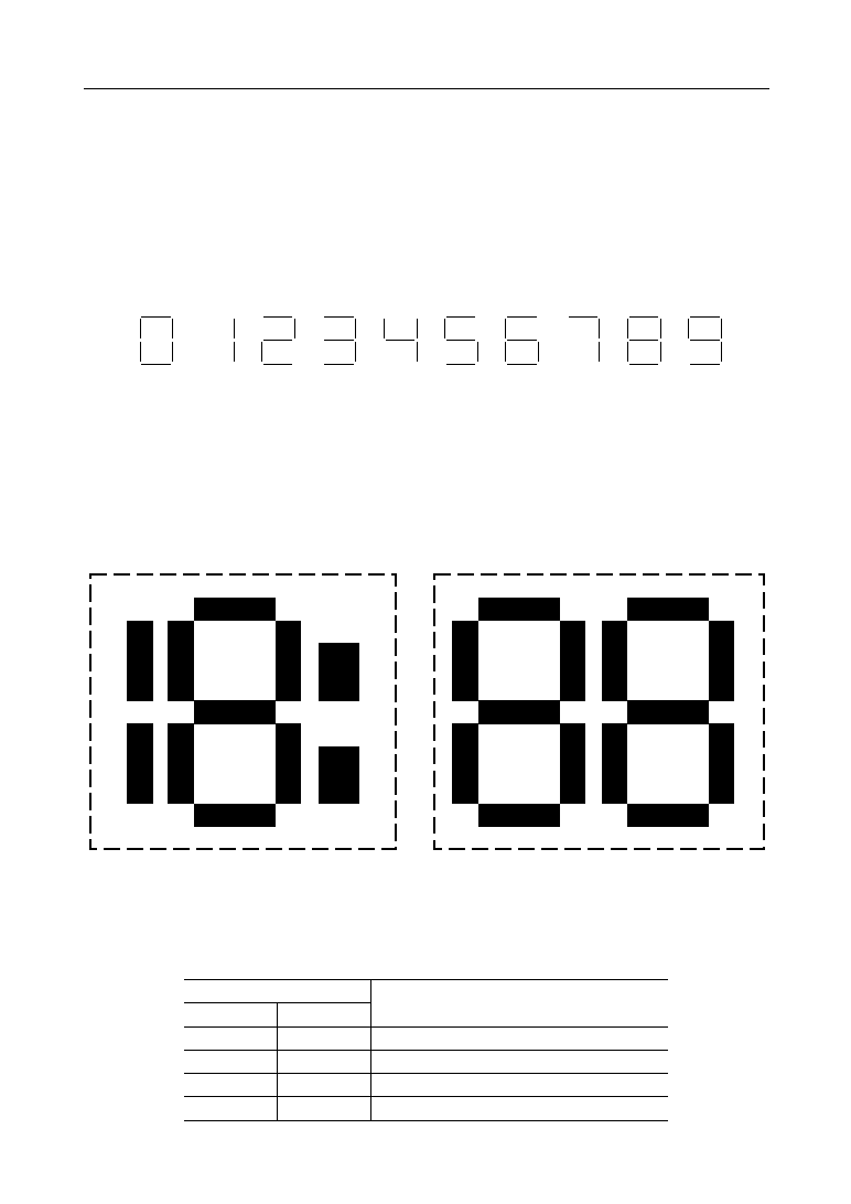
∑ 7 Segment Display
∑ Display Device
Dynamic drive 4-digit fluorescent display (with colons)
∑ Relationship between Amode & Grid Outputs and VF display Tube
∑ Luminance Switch Function
4-degree switchable luminance (frequency = 250 Hz, gap width between GR1 and GR2 = 30
µ
s)
f = 250 Hz 1/2 Duty (50% display)
DIM2
Operation mode
Switch pin name
DIM1
L
H
L
L
L
H
H
H
(25% display)
(12.5% display)
(6.25% display)
GR2
GR1
4b
3f
4c
3e
3b
col
or
col'
col
or
col'
3a
3g
3d
3c
2f
2e
2b
2a
2g
2d
2c
1f
1e
1b
1a
1g
1d
1c
RELATIONSHIP BETWEEN ANODE & GRID OUTPUTS AND VF DISPLAY TUBE

7/11
MSC1210
° Semiconductor
FEDL1210-03
∑ Display Mode
4-digit display of hours/minutes on a 12-hour format.
Hours display ............. between 1 and 12
Minutes display .......... between 00 and 59
The most significant digit will not appear if it is zero. (Most significant digit zero suppress
mechanism)
∑ Correcting Clock
Hour/minute fast advance function.
Hour digits and minute digits can fast advance, separately.
The hour digit can fast advance via HS pin (Hour Set), and the minute digit via MS pin (Minute
Set) with 2 Hz period.
The hour counter or minute counter is incremented by 1 each time of pressing.
If keeping it depressed, these counters are incremented continuously with 2 Hz intervals.
The HS and MS pins, when they are open, are kept at "1" level with a pull-up resistor, and
become non-active.
These pins become active when "0" level voltage is supplied from the external source.
The hour digit and minute digit can fast advance simultaneously.
In doing the fast advance operation, the low order digit of the counter continues a normal
operation, but a carry out of the minute digit into the hour digit does not occur.
In doing the minute digit fast advance, a carry into the hour digit does not occur.
∑ Zero Adjust Function (
±
30 minutes Zero Reset)
The ZA pin (Zero Adjust), when it is open, is kept at "1" level thith a pull-up resisitor, and
becomes non-active.
This pin becomes active when "0" level voltage is supplied from the external source in order
to execute Zero Adjust operation.
If the minute digits are smaller than 30, the minute digits and second digits are reset to 00'00".
If the minute digits are larger than 30, the minute digits and second digits are reset to 00'00",
and a carry into the hour digit is executed.
Pre-second resetting of the counter is performed up to 16 Hz.
(Zero Adjust Example)
(X ≠ 1) (hour) 30'00"
X (hour) 00'00" X (hour) 00'00"
X (hour) 29'59"
X (hour) 30'00"
X (hour) 59'59" (X + 1) (hour) 00'00"
(X + 1) (hour) 29'59"

8/11
MSC1210
° Semiconductor
FEDL1210-03
∑ Blanking of Display
The display is blanked by externally applying "0" level voltage to BLANK pin.
∑ 64 Hz Pin
Output pin for oscillation frequency adjustment.
This pin always outputs a frequency of 64 Hz.
∑ Constant-Voltage Circuit
The constant-voltagae circuit supplys the logic section with a voltage down to between 3.4 V
and 5 V from between 4 V and 18 V.
∑ Power On Reset
No external capacitor is needed since the IC contains a capacitor.
∑ Test Pin
Used to test the IC.
∑ Removal of Chattering
The MS, HS, and ZA input pins contains a chattering removal circuit, so that chattering of less
than 31.25 msec is removable inside of the IC.

9/11
MSC1210
° Semiconductor
FEDL1210-03
(Unit : mm)
PACKAGE DIMENSIONS
Notes for Mounting the Surface Mount Type Package
The SOP, QFP, TSOP, TQFP, LQFP, SOJ, QFJ (PLCC), SHP, and BGA are surface mount type
packages, which are very susceptible to heat in reflow mounting and humidity absorbed in
storage. Therefore, before you perform reflow mounting, contact Oki's responsible sales person
on the product name, package name, pin number, package code and desired mounting conditions
(reflow method, temperature and times).
SSOP32-P-430-1.00-K
Mirror finish
Package material
Lead frame material
Pin treatment
Package weight (g)
Oki Electric Industry Co., Ltd.
Rev. No./Last Revised
Epoxy resin
42 alloy
Solder plating (5 mm)
0.60 TYP.
3/Dec. 5, 1996

10/11
MSC1210
° Semiconductor
FEDL1210-03
(Unit : mm)
SDIP30-P-400-1.778
Package material
Lead frame material
Pin treatment
Package weight (g)
Oki Electric Industry Co., Ltd.
Rev. No./Last Revised
Epoxy resin
42 alloy
Solder plating (5 mm)
1.80 TYP.
2/Dec. 11, 1996

11/11
MSC1210
° Semiconductor
FEDL1210-03
NOTICE
1.
The information contained herein can change without notice owing to product and/or
technical improvements. Before using the product, please make sure that the information
being referred to is up-to-date.
2.
The outline of action and examples for application circuits described herein have been
chosen as an explanation for the standard action and performance of the product. When
planning to use the product, please ensure that the external conditions are reflected in the
actual circuit, assembly, and program designs.
3.
When designing your product, please use our product below the specified maximum
ratings and within the specified operating ranges including, but not limited to, operating
voltage, power dissipation, and operating temperature.
4.
Oki assumes no responsibility or liability whatsoever for any failure or unusual or
unexpected operation resulting from misuse, neglect, improper installation, repair, alteration
or accident, improper handling, or unusual physical or electrical stress including, but not
limited to, exposure to parameters beyond the specified maximum ratings or operation
outside the specified operating range.
5.
Neither indemnity against nor license of a third party's industrial and intellectual property
right, etc. is granted by us in connection with the use of the product and/or the information
and drawings contained herein. No responsibility is assumed by us for any infringement
of a third party's right which may result from the use thereof.
6.
The products listed in this document are intended for use in general electronics equipment
for commercial applications (e.g., office automation, communication equipment,
measurement equipment, consumer electronics, etc.). These products are not authorized
for use in any system or application that requires special or enhanced quality and reliability
characteristics nor in any system or application where the failure of such system or
application may result in the loss or damage of property, or death or injury to humans.
Such applications include, but are not limited to, traffic and automotive equipment, safety
devices, aerospace equipment, nuclear power control, medical equipment, and life-support
systems.
7.
Certain products in this document may need government approval before they can be
exported to particular countries. The purchaser assumes the responsibility of determining
the legality of export of these products and will take appropriate and necessary steps at their
own expense for these.
8.
No part of the contents contained herein may be reprinted or reproduced without our prior
permission.
9.
MS-DOS is a registered trademark of Microsoft Corporation.
Copyright 2000 Oki Electric Industry Co., Ltd.
Printed in Japan