 | –≠–ª–µ–∫—Ç—Ä–æ–Ω–Ω—ã–π –∫–æ–º–ø–æ–Ω–µ–Ω—Ç: AWS5508 | –°–∫–∞—á–∞—Ç—å:  PDF PDF  ZIP ZIP |

08/2001
Table 1: Pin Description
FEATURES
∑
2.7V Control Operation
∑
Tri-band Operation
∑
High Isolation
∑
High Power
∑
High Linearity
∑
Small Leadless Package
APPLICATIONS
∑
SP4T Antenna switch operating in the GSM
900 MHz, DCS 1800 MHz, and PCS 1900 MHz
bands
AWS5508
SP4T PHEMT
Transmit/Receive Antenna Switch
GSM 900 MHz/DCS 1800 MHz/PCS 1900 MHz
ADVANCED PRODUCT INFORMATION - Rev 0.3
PRODUCT DESCRIPTION
The AWS5508 SP4T high power antenna switch is
designed to operate in the GSM 900Mhz, DCS
1800MHz, and PCS 1900MHz frequency bands. All 4
ports of the switch have identical electrical and
linearity performance which allows flexibility in
system design. Switching between ports is
accomplished using 2.7 to 6 volts differential control
voltages on the 4 control pins. The switch is provided
in a leadless MLP-16 quad flat package.
S19
MLP-16 Multipin Leadless
Plastic Package
PIN
NAME
DESCRIPTION
PIN
NAME
DESCRIPTION
1
V1
Control for RF1 , pin 2.
9
RF3
RF port, controlled by V3.
2
RF1
RF port, controlled by V1.
10
GND
Ground connection, keep short as possible.
3
GND
Ground connection, keep short as possible.
11
GND
Ground connection, keep short as possible.
4
RF2
RF port, controlled by V2.
12
RF4
RF port, controlled by V4.
5
GND
Ground connection, keep short as possible.
13
GND
Ground connection, keep short as possible.
6
V2
Control for RF2, pin 4.
14
V4
Control for RF4, pin 12.
7
V3
Control for RF3, pin 9.
15
GND
Ground connection, keep short as possible.
8
GND
Ground connection, keep short as possible.
16
RFc
Common RF Port.
Figure 1: Pin Out Diagram
1
2
3
4
5
6
7
8
9
10
11
12
13
14
15
16
GND
GND
GND
GND
GND
GND
GND
V1
V4
V2 V3
Vs
Optional Rs
Note 3
C
b
C
b
C
b
C
b
C
b
RF
c
RF
1
RF
2
RF
3
RF
4
TOP VIEW
AWS5508
PIN 1 INDICATOR
1. DC blocking capacitors C
b
and optional
resistor Rs must be supplied externally.
2. C
b
= 100 pF for operation >500MHz.
3. The use of resistor Rs to the positive
voltage supply is optional. It is only required
if it is necessary to have all RF ports in Isolation
state at the same time. Also, using Rs will improve
linearity performance to a small degree when V
CTL
is at its lower limit. Rs = 10k when used.

ADVANCED PRODUCT INFORMATION - Rev 0.3
08/2001
2
AWS5508
Table 3: Operating Ranges at 25∞ C
Notes:
1.
All measurements made in a broadband 50
system.
2.
Video feedthru measured with 1 ns risetime pulse and 500MHz bandwidth.
3.
VCTL is the differential voltage between any one of the control pins (V1 through V4) and the remaining three
control pins. Changing which control pin is the most positive voltage selects the switch path as defined in the
truth table below. Use of the optional resistor Rs on the common port limits VHigh to Vs ± 0.2V.
PARAMETER
CONDITION
FREQUENCY
MIN
TYP
MAX
UNIT
Switching Characteristics
Rise, Fall (10/90% or 90/10% RF)
On, Off (50% CTL to 90%/10% RF)
Video Feedthru
100
100
50
ns
ns
mV
Intermodulation Intercept Point (IP3)
2 tone power levels 13dBm to 27dBm
(selected to optimize dynamic range of
test)
V
CTL
= 2.7V
1.0 GHZ
+48
+51
dBm
1.8 GHz
+48
+51
dBm
V
CTL
= 5.0V
1.0 GHz
+56
+59
dBm
1.8 GHz
+56
+60
dBm
Control Voltage (VCTL)
3
2.7
6
V
Leakage Current
V
CTL
= 2.7V
>5
50
µA
V
CTL
= 5.0V
>10
100
µA
The device may be operated safely over these conditions; however, parametric performance is guaranteed
only over the conditions defined in the electrical specifications.
ELECTRICAL CHARACTERISTICS
Table 2: Absolute Minimum and Maximum Ratings
Notes:
1. Control Voltage is the diffenterial voltage between any of pins V1,
V2, V3, V4 and RFc.
Stresses in excess of the absolute ratings may cause permanent
damage. Functional operation is not implied under these
conditions. Exposure to absolute ratings for extended periods
of time may adversely affect reliability.
PARAMETER
MIN
MAX
UNIT
RF Input Power
> 500 MHz, VCTL = 2.7V
-
8
W
Control Voltage
-0.4
10
V
Operating Temperature
-40
+125
∞C
Storage Temperature
-65
+150
∞C

ADVANCED PRODUCT INFORMATION - Rev 0.3
08/2001
3
AWS5508
Table 6: Functional Truth Table
V
CTL
= V
HIGH
- V
LOW
= +2.5V to +8V (V
HIGH
= Vs 0.2V when Rs is used on RF
C
port.)
±
V1
V2
V3
V4
RFc RF1
RFc RF2
RFc RF3
RFc RF4
V
HIGH
V
LOW
V
LOW
V
LOW
Low Loss
Isolation
Isolation
Isolation
V
LOW
V
HIGH
V
LOW
V
LOW
Isolation
Low Loss
Isolation
Isolation
V
LOW
V
LOW
V
HIGH
V
LOW
Isolation
Isolation
Low Loss
Isolation
V
LOW
V
LOW
V
LOW
V
HIGH
Isolation
Isolation
Isolation
Low Loss
Table 5: Harmonics
1. Measured in broadband 50 system
CONTROL VOLTAGE
(V
CTL
)
HARMONIC LEVEL (DBC) TYP.
(1)
1000MHz, Pin = +34dBm 2000MHz, Pin = +34dBm
2nd
3rd
2nd
3rd
2.7V
-58
-61
-59
-60
4.7V
-63
-64
-61
-63
Table 4: Electrical Specifications at 25 ∞C (V
CTL
= 2.7V)
PARAMETER
CONDITION
FREQUENCY
MIN
TYP
MAX
UNIT
Insertion Loss
P
IN
= +34dBm
0.5 - 1.0 GHz
1.0 - 2.0 GHz
0.65
0.90
0.8
1.0
dB
dB
Isolation
P
IN
= +34dBm
0.5 - 1.0 GHz
1.0 - 2.0 GHz
22
18
25
21
dB
dB
VSWR
In Low Loss Path
0.5 - 2.0 GHz
1.20:1
1.35:1

ADVANCED PRODUCT INFORMATION - Rev 0.3
08/2001
4
AWS5508
PERFORMANCE DATA
Figure 2: Insertion Loss vs. Frequency
Figure 3: Isolation vs. Frequency
Figure 4:Return Loss vs. Frequency
Figure 5: TOI vs Control Voltage
Figure 6: 2nd and 3rd Harmonic Levels vs Control
Voltage at 1.0 GHz @ +34dBm
-1.2
-1.0
-0.8
-0.6
-0.4
-0.2
0.0
0.5
1.0
1.5
2.0
2.5
Frequency (GHz)
Inseriton Loss (dB)
Isolation vs. Frequency
-35
-30
-25
-20
-15
-10
-5
0
0.5
1.0
1.5
2.0
2.5
Frequency (GHz)
Isolation (dB)
Return Loss vs. Frequency
-30
-25
-20
-15
-10
-5
0
0.5
1.0
1.5
2.0
2.5
Frequency (GHz)
Return Loss (dB)
TOI vs Control Voltage
0
10
20
30
40
50
60
70
2.5
3.0
3.5
4.0
4.5
5.0
Control Voltage (V)
TOI (dBm)
1.00GHz
1.88GHz
-70
-60
-50
-40
-30
-20
-10
0
2
2.5
3
3.5
4
4.5
5
Control Voltage (V)
Harmonic Level (dBc)
2nd Harmonic
3rd Harmonic
-70
-60
-50
-40
-30
-20
-10
0
2.0
2.5
3.0
3.5
4.0
4.5
5.0
Control Voltage (V)
Harmonic Level (dBc)
2nd Harmonic
3rd Harmonic
Figure 7: 2nd and 3rd Harmonic Levels vs Control
Voltage at 2.0 GHz @ +34dBm
ADVANCED PRODUCT INFORMATION - Rev 0.3
08/2001
5
AWS5508
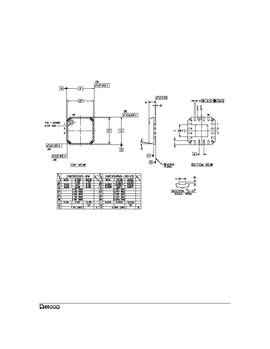
Figure 8: Package Outline Drawing
PACKAGE OUTLINE

ADVANCED PRODUCT INFORMATION - Rev 0.3
08/2001
6
AWS5508
NOTES

ADVANCED PRODUCT INFORMATION - Rev 0.3
08/2001
7
AWS5508
NOTES

ADVANCED PRODUCT INFORMATION - Rev 3
08/2001
8
IMPORTANT NOTICE
ANADIGICS, Inc. reserves the right to make changes to its products or to discontinue any product at any time without
notice. The product specifications contained in Advanced Product Information sheets and Preliminary Data Sheets are
subject to change prior to a product's formal introduction. Information in Data Sheets have been carefully checked and are
assumed to be reliable; however, ANADIGICS assumes no responsibilities for inaccuracies. ANADIGICS strongly urges
customers to verify that the information they are using is current before placing orders.
WARNING
ANADIGICS products are not intended for use in life support appliances, devices, or systems. Use of an ANADIGICS
product in any such application without written consent is prohibited.
ANADIGICS, Inc.
141 Mount Bethel Road
Warren, New Jersey 07059, U.S.A
Tel: +1 (908) 668-5000
Fax: +1 (908) 668-5132
http://www.anadigics.com
Mktg@anadigics.com
AWS5508
ORDERING INFORMATION
ORDER NUMBER
PACKAGE DESCRIPTION
COMPONENT PACKAGING
AWS5508S19
S19
Multipin Leadless Plastic Package