 | –≠–ª–µ–∫—Ç—Ä–æ–Ω–Ω—ã–π –∫–æ–º–ø–æ–Ω–µ–Ω—Ç: AGB3301 | –°–∫–∞—á–∞—Ç—å:  PDF PDF  ZIP ZIP |

06/2003
AGB3301
50W
High Linearity Low Noise
Wideband Gain Block
Data Sheet - Rev 2.0
S24 Package
SOT-89
FEATURES
∑ 250-3000 MHz Frequency Range
∑ +45 dBm Output IP3
∑ Low Noise Figure: 2.4 dB at 900 MHz
∑ 13.5 dB Gain at 900 MHz
∑ +24 dBm P1dB
∑ SOT-89 Package
∑ Single +5V to +9V Supply
∑ Low Power: less than 1 Watt
∑ Case Temperature: -40 to +100
o
C
APPLICATIONS
∑ Cellular Base Stations for W-CDMA, CDMA,
TDMA, GSM, PCS and CDPD systems
∑ Fixed Wireless
∑ MMDS/WLL
∑ WLAN, HyperLAN
∑ CATV
PRODUCT DESCRIPTION
The AGB3301 is one of a series of GaAs MESFET
amplifiers designed for use in applications
requiring high linearity, low noise and low distortion.
With a high output IP3, low noise figure and wide
band operation, the AGB3301 is ideal for 50W
wireless infrastructure applications such as Cellular
Base Stations, MMDS, and WLL. Offered in a low
cost SOT-89 surface mount package, the AGB3301
requires a single +5V to +9V supply, and typically
consumes less than 1 Watt of power.
Figure 1: Block Diagram
RF Output
/ Bias
RF Input

2
Data Sheet - Rev 2.0
06/2003
AGB3301
N
I
P
E
M
A
N
N
O
I
T
P
I
R
C
S
E
D
1
F
R
N
I
t
u
p
n
I
F
R
2
D
N
G
d
n
u
o
r
G
3
F
R
T
U
O
s
a
i
B
/
t
u
p
t
u
O
F
R
4
D
N
G
d
n
u
o
r
G
Figure 2: Pin Out
Table 1: Pin Description
2
3
1
4
RF
IN
RF
OUT
GND
GND
Data Sheet - Rev 2.0
06/2003
3
AGB3301
ELECTRICAL CHARACTERISTICS
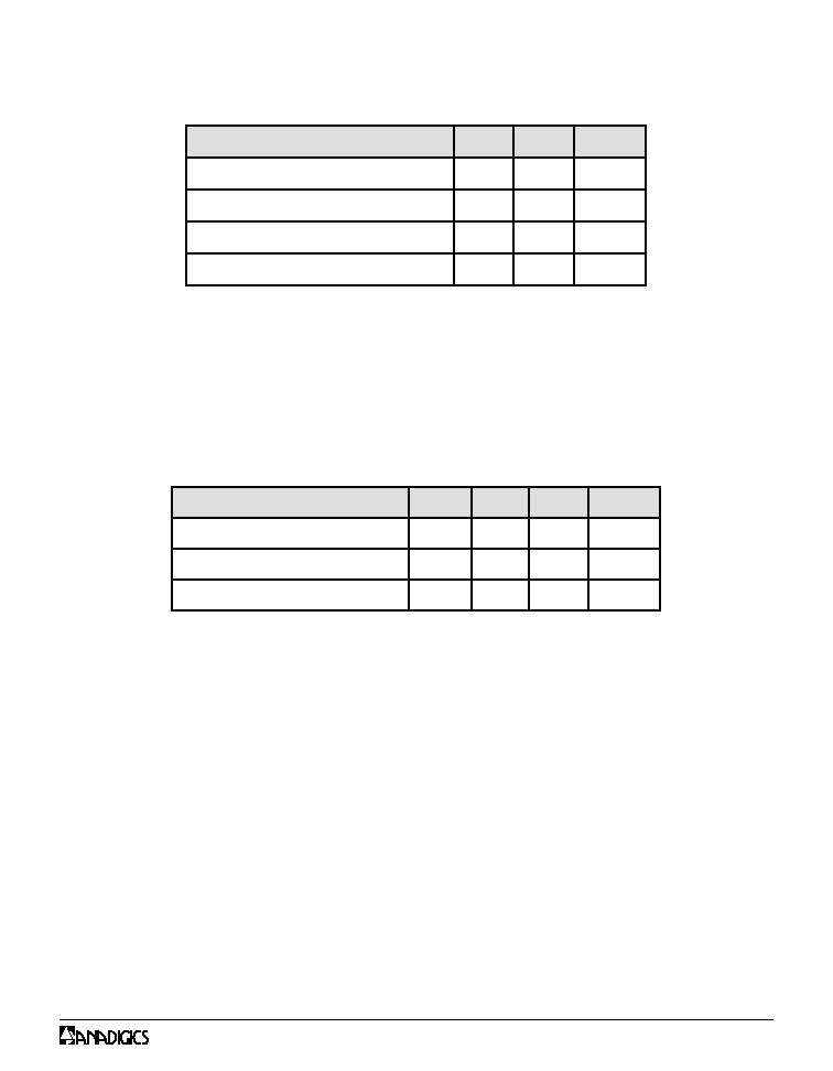
Table 2: Absolute Minimum and Maximum Ratings
R
E
T
E
M
A
R
A
P
N
I
M
X
A
M
T
I
N
U
e
g
a
tl
o
V
e
c
iv
e
D
0
2
1
+
C
D
V
r
e
w
o
P
t
u
p
n
I
F
R
-
5
1
+
m
B
d
e
r
u
t
a
r
e
p
m
e
T
e
g
a
r
o
t
S
0
4
-
0
5
1
+
C
∞
e
r
u
t
a
r
e
p
m
e
T
l
e
n
n
a
h
C
-
0
5
1
+
C
∞
Stresses in excess of the absolute ratings may cause permanent
damage. Functional operation is not implied under these conditions.
Exposure to absolute ratings for extended periods of time may
adversely affect reliability.
Table 3: Operating Ranges
The device may be operated safely over these conditions; however,
parametric performance is guaranteed only over the conditions defined
in the electrical specifications.
R
E
T
E
M
A
R
A
P
N
I
M
P
Y
T
X
A
M
T
I
N
U
f
:
y
c
n
e
u
q
e
r
F
g
n
it
a
r
e
p
O
0
5
2
-
0
0
0
3
z
H
M
V
:
e
g
a
tl
o
V
e
c
iv
e
D
DD
-
9
+
0
1
+
C
D
V
T
:
e
r
u
t
a
r
e
p
m
e
T
e
s
a
C
c
0
4
-
-
0
0
1
+
o
C

4
Data Sheet - Rev 2.0
06/2003
AGB3301
Table 4: Electrical Specifications - Unmatched 50W Test Circuit
(T
A
= +25
∞C, V
DD
= +9 VDC, f = 900 MHz, see Figure 3)
Notes:
(1) OIP3 is measured with two tones: 900 MHz and 901 MHz, +5dBm output per
tone.
Figure 3: Unmatched 50W Test Circuit
V
DD
AGB3301
RF Choke
DC Block
DC Block
Bypass
RF
Input
RF
Output
V
SUPPLY
R
E
T
E
M
A
R
A
P
N
I
M
P
Y
T
X
A
M
T
I
N
U
S
:
n
i
a
G
1
2
2
1
5
.
3
1
5
1
B
d
S
:
s
s
o
L
n
r
u
t
e
R
t
u
p
n
I
1
1
-
5
1
-
0
1
-
B
d
S
:
s
s
o
L
n
r
u
t
e
R
t
u
p
t
u
O
2
2
-
5
1
-
0
1
-
B
d
3
P
I
t
u
p
t
u
O
)
1
(
2
4
+
5
4
+
-
m
B
d
e
r
u
g
i
F
e
s
i
o
N
-
4
.
2
5
.
3
B
d
B
d
1
P
:
n
o
i
s
s
e
r
p
m
o
C
B
d
1
t
u
p
t
u
O
-
4
2
+
-
m
B
d
:
e
c
n
a
t
s
i
s
e
R
l
a
m
r
e
h
T
-
-
0
4
o
W
/
C
t
n
e
rr
u
C
y
l
p
p
u
S
0
9
0
1
1
0
3
1
A
m
q
JC

Data Sheet - Rev 2.0
06/2003
5
AGB3301
PERFORMANCE DATA
Figures 4 through 8 contain data for the device as tested in the unmatched 50W test circuit shown in Figure 3.
Unless otherwise indicated, V
DD
= +9 VDC.
Figure 4: OIP3 vs. Frequency
(in Unmatched 50W Test Circuit)
Figure 8: Return Loss vs. Frequency
(in Unmatched 50W Test Circuit)
Figure 5: OIP3 vs. Case Temperature
(in Unmatched 50W Test Circuit)
Figure 6: Gain vs. Frequency
(in Unmatched 50W Test Circuit)
Figure 7: Gain vs. Case Temperature
(in Unmatched 50W Test Circuit)
25
30
35
40
45
50
-50
-25
0
25
50
75
100
Case Temperature (
o
C)
OIP
3
(dB
m
)
Output Power = +5 dBm
Frequency = 900 MHz
11
11 .5
12
12 .5
13
13 .5
14
-50
-25
0
25
5 0
75
10 0
Case T emp erture (
o
C )
G
a
in
(d
B
)
F requenc y = 9 00 M Hz
-40
-35
-30
-25
-20
-15
-10
-5
0
5
0
300
600
900
1200
1500
1800
2100
2400
2700
3000
Frequency (MHz)
R
e
tur
n
Los
s
(dB
)
S11
S22
T
A
= +25
o
C
0
2
4
6
8
10
12
14
16
0
300
600
900
1200
1500
1800
2100
2400
2700
3000
Frequency (MHz)
G
a
in (
d
B)
T
A
= +25
o
C
25
30
35
40
45
50
0
300
600
900
1200
1500
1800
2100
2400
2700
3000
Frequency (MHz)
OI
P3
(
d
B
m
)
Output Power = +5 dBm
T
A
= +25
o
C