AH266
High Voltage Hall Effect Latch
This datasheet contains new product information. Anachip Corp. reserves the rights to modify the product specification without notice. No liability is assumed as a result of the use of
this product. No rights under any patent accompany the sale of the product.
Rev. 0.1 Mar 25, 2004
1/6
Features
- On-chip Hall plate
- Operating voltage: 4V~28V
- Output current: 400mA(Continuous, 25
o
C)
- Reverse protection diode only for chip reverse
power connecting
(Note)
- Output protection Zener breakdown Vz=62V(Typ)
- Package: SIP-4L
(Note)
Protection diode only exists at power pin(1,4) output, not
including pin (2,3).
Application
- Dual-coil Brush-less DC Motor
- Dual-coil Brush-less DC Fan
- Revolution Counting
- Speed Measurement
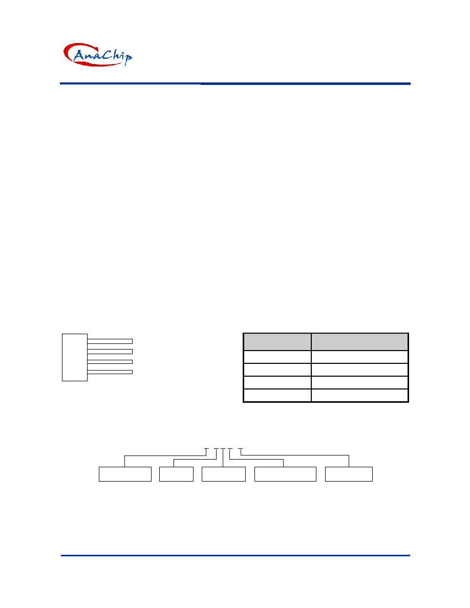
Pin Assignment
1. VCC
2. DO
4. GND
3. DOB
General Description
AH266 is an integrated Hall sensor with output
drivers designed for electronic commutation of
brush-less DC motor applications. The device
includes an on-chip Hall voltage generator for
magnetic sensing, a comparator that amplifies the
Hall voltage, and a Schmitt trigger to provide
switching hysteresis for noise rejection, and
complementary darlington open-collector drivers for
sinking large current loads. An internal bandgap
regulator is used to provide temperature
compensated supply voltage for internal circuits and
allows a wide operating supply range.
If a magnetic flux density (B) is larger than operate
point (Bop), DO turn on (low) and DOB turn off
(high). The outputs state is latched prior to reach
release point (Brp). if B< Brp, DO turn off and DOB
turn on. ATS266 is rated for operation over
temperature range from -20
o
C to 85
o
C and voltage
range from 4V to 28V. The devices are available in
low cost die forms or rugged 4 pin SIP packages.
Pin Configuration
Name
Description
VCC
Positive Power Supply
DO
Output Pin
DOB
Output Pin
GND
Ground
Ordering Information
AH266 X - X X X - X
Packing
Blank : Tube
A : Taping
P: SIP-4L
Package
Lead
L : Lead Free
Blank: Normal
Wafer Body
Magnetic
Characteristics
Blank or
A~Z : if necessary
to specify
A or B

AH266
High Voltage Hall Effect Latch
Anachip Corp.
www.anachip.com.tw
Rev 0.1 Mar 25, 2004
2/6
Block Diagram
1
REG.
Hall
Plate
Amp
VCC
DO
DOB
Application Circuit
1 2
4
3
266
coil1
coil2
Vcc
Brush-less DC Fan
Note: This application circuit can't protect reverse coil current if power is connecting reverse.

AH266
High Voltage Hall Effect Latch
Anachip Corp.
www.anachip.com.tw
Rev 0.1 Mar 25, 2004
3/6
Absolute Maximum Ratings
(at Ta = 25
0
C )
Parameter
Symbol
Rating
Unit
Supply voltage
VCC
28
V
Output "OFF " voltage
Vout (off)
28
V
Io (con)
400 (Note 1)
mA
Io (hold)
500
mA
Output "ON" current
Io (peak)
700
mA
Magnetic flux density
B
Unlimited
Gauss
Operating temperature range
Top
-20~+85
�C
Storage temperature range
Tstg
-65~+150
�C
Power dissipation (Note 2)
PD 550
mW
Note 1: Io(con) is 150 mA at 85
�C
2: See Performance Characteristic for other conditions
Electrical Characteristics
( Ta = 25
�C )
Characteristic
Symbol
Conditions
Min
Typ
Max
Unit
Supply Voltage
Vcc
4
28 V
Output Zener Breakdown
Vz
Output Turn off
54
62
70
V
Output Saturation Voltage
Vce(sat) Vcc=24V, Ic=400mA
1.1 1.5 V
Output Leakage Current
Icex
Vce=24V, Vcc=24V
< 0.1
10 �A
Supply Current
Icc
Vcc=24V, Output Open
5
10
mA
Output Rise Time
tr
Vcc=24V, RL=820
, CL=20pF
1.0 5 �s
Output Falling Time
tf
Vcc=24V, RL=820
, CL=20pF
1.0 1.5 �s
Switch Time Differential
t Vcc=24V,
RL=820
, CL=20pF
3.0 10 �s
Test Circuit
266
CL1
CL2
24V
Vout1(DO)
Vout2(DOB)
RL1=RL2=820 Ohm
CL1=CL2=20 pF
RL2
RL1

AH266
High Voltage Hall Effect Latch
Anachip Corp.
www.anachip.com.tw
Rev 0.1 Mar 25, 2004
4/6
Magnetic Characteristics
(Ta=+25
o
C)
(1mT = 10 Gauss)
A grade
Characteristic
Symbol
Min.
Typ.
Max.
Unit
Operate Point
Bop
10
-
70
Gauss
Release Point
Brp
-70
-
-10
Gauss
Hysteresis Bhy
-
80
-
Gauss
B grade
Characteristic
Symbol
Min.
Typ.
Max.
Unit
Operate Point
Bop
-
-
100
Gauss
Release Point
Brp
-100
-
-
Gauss
Hysteresis Bhy
-
80
-
Gauss
Output Voltage in Volts
Output Voltage in Volts
0
0
Magnetic Flux Density in Gauss
Magnetic Flux Density in Gauss
DO
DOB
Bop
Bop
Brp
Brp
B
hy
Turn on
Turn off
B
hy
Turn off
Turn on
Vsat
Vsat
Performance Characteristics (SIP-4L)
Ta (
�C)
25
50
60
70
80
85
90
95
100
105
110
115
120
Pd
(mW) 550 440 396 352 308 286 264 242 220 198 176 154 132
Power Dissipation Curve
0
200
400
600
800
1000
0
25
50
75
100
125
150
Ta (C)
Pd (mW)
85

AH266
High Voltage Hall Effect Latch
Anachip Corp.
www.anachip.com.tw
Rev 0.1 Mar 25, 2004
5/6
Operation Characteristics
Marking side
S
B
hy
V
sat
V
cc
( Output Voltage )
V
d
B
rp
B
op
0
S
N
( Magnetic flux density )
DO
High
Low
( SIP4 )
N
Marking Information
266
Part Number
Year:
( Front View )
"2" = 2002
"1" = 2001
X XX X X
Nth week: 01~52
ID Code: A ~ Z
Blank: normal
L: Lead Free Package
