 | ÐлекÑÑоннÑй компоненÑ: A8032 | СкаÑаÑÑ:  PDF PDF  ZIP ZIP |
Äîêóìåíòàöèÿ è îïèñàíèÿ www.docs.chipfind.ru

A8032 Series
Preliminary
8 Bit Microcontroller
PRELIMINARY (November,
1998, Version 0.0)
AMIC Technology, Inc.
Document Title
8 Bit Microcontroller
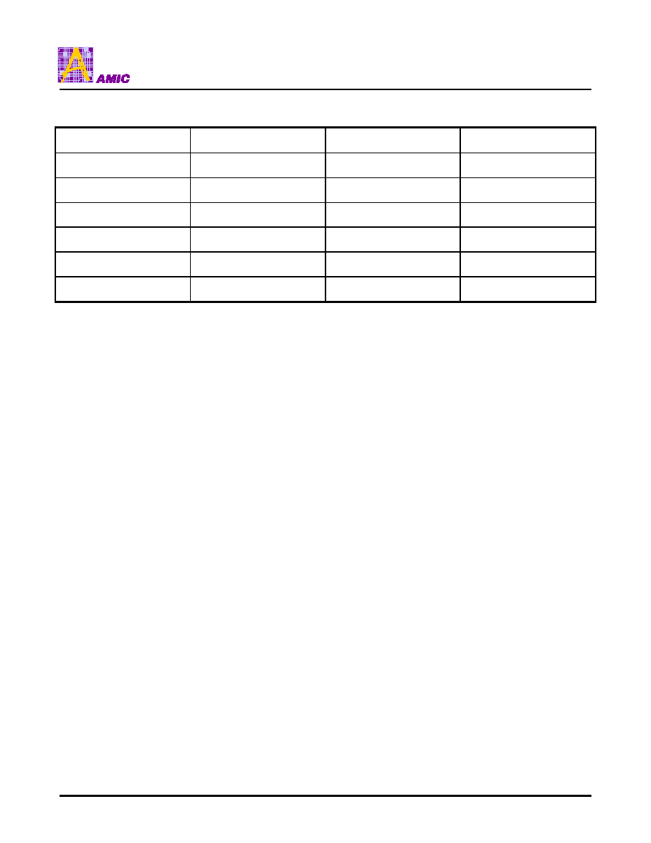
Revision History
Rev. No.
History
Issue Date
Remark
0.0
Initial issue
November 27, 1998
A8032 Series
Preliminary
8 Bit Microcontroller
PRELIMINARY (November,
1998, Version 0.0)
1
AMIC Technology, Inc.
Features
n
8-bit CMOS microcontroller
n
Fully static design with power saving idle mode and
power down mode
n
Low standby current at full supply voltage
n
Versions for 12/24/40MH
Z
operating frequency
n
On chip 256B RAM
n
Four 8-bit bidirectional ports
n
Three 16-bit Timers/Counters (Timer 2 with up/down
counter feature)
n
One full duplex serial port
n
Boolean processor
n
Six interrupt sources, two priority levels
n
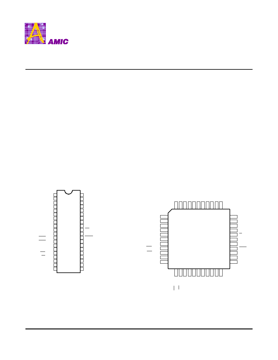
Available in 40-pin P-DIP and 44-pin PLCC packages
n
64K bytes external data memory space
General Description
The AMIC A8032 is a high-performance 8-bit
microcontroller. It is compatible with the industry
standard 80C52 microcontroller series.
The A8032 contains a 256B RAM, four 8-bit bidirectional
parallel ports, three 16-bit timer/counters, a serial port
and six interrupt sources with two priority levels.
The A8032 has supports 64KB external data memory.
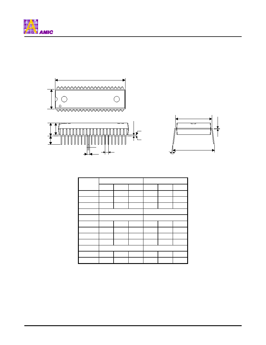
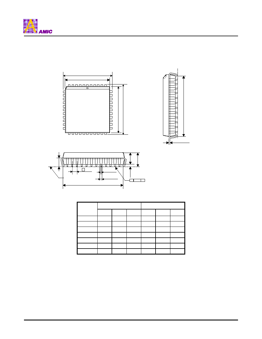
Pin Configurations
n
P-DIP
n
PLCC
T2,P1.0
T2EX,P1.1
P1.2
TXD,P3.1
XTAL2
XTAL1
GND
P0.2,AD2
P0.1,AD1
P0.0,AD0
VCC
A8032
21
P0.3,AD3
P1.3
P1.4
P1.6
P1.7
RST
RXD,P3.0
T1,P3.5
INT0,P3.2
P1.5
PSEN
ALE
EA
P0.7,AD7
P0.6,AD6
P0.5,AD5
P0.4,AD4
20
19
18
12
16
17
13
14
15
11
10
9
8
7
6
5
4
3
2
1
22
23
24
25
26
27
28
29
30
31
32
33
34
35
36
37
38
39
40
A8032L
P1.5
P1.4
INT1,P3.3
T0,P3.4
WR,P3.6
RD,P3.7
P2.7,A15
P2.6,A14
P2.5,A13
P2.4,A12
P2.3,A11
P2.2,A10
P2.1,A9
P2.0,A8
P1.3
P1.2
P1.1,T2EX
P1.0,T2
GND
VCC
P0.0,AD0
P0.1,AD1
P0.2,AD2
P0.3,AD3
P1.6
P1.7
RST
RXD,P3.0
NC
TXD,P3.1
INT0, P3.2
INT1,P3.3
T0,P3.4
T1,P3.5
P0.4,AD4
EA
NC
ALE
PSEN
P2.7,A15
P2.6,A14
P2.5,A13
28
27
26
25
24
23
22
21
20
19
18
44
43
42
41
40
1
2
3
4
5
6
39
38
37
36
35
34
33
32
31
30
29
7
8
9
10
11
12
13
14
15
16
17
P0.5,AD5
P0.6,AD6
P0.7,AD7
WR,P3.6
RD,P3.7
XTAL2
XTAL1
GND
NC
P2.0,A8
P2.1,A9
P2.2,A10
P2.3,A11
P2.4,A12
A8032 Series
PRELIMINARY (November,
1998, Version 0.0)
2
AMIC Technology, Inc.
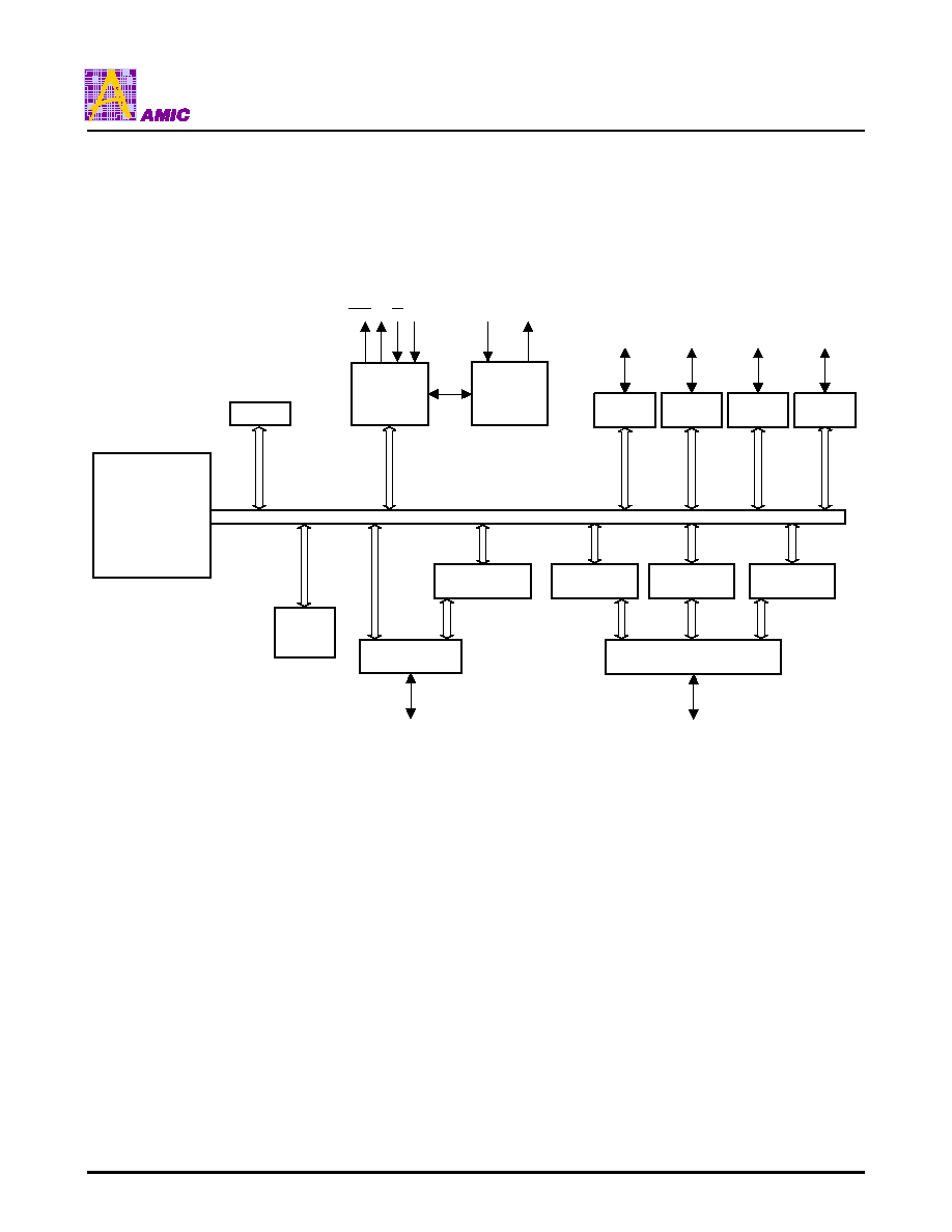
Block Diagram
CPU CORE
TIMING AND
CONTROL
SFR
PSEN ALE EA
RST
OSCILLATOR
XTAL1
XTAL2
PORT 0
P0.0-P0.7
ADDRESS
(AD0-AD7)
PORT 2
P2.0-P2.7
ADDRESS
A8-A15
256B
RAM
PORT 1
TIMER 2
INTERRUPT
SERIAL PORT
TIMER 0.1
PORT 3
P1.0-P1.7
P3.0-P3.7
A8032 Series
PRELIMINARY (November,
1998, Version 0.0)
3
AMIC Technology, Inc.
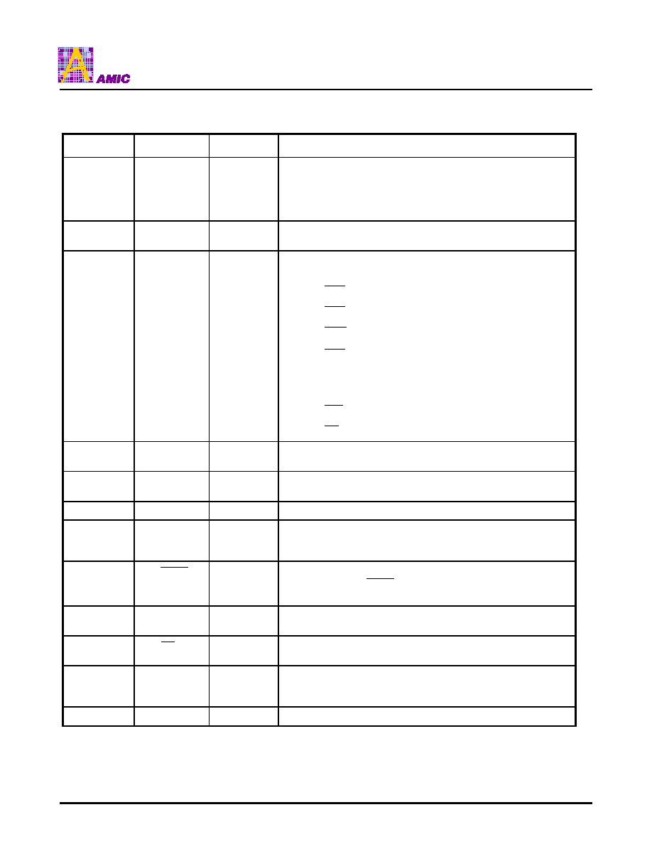
Pin Description
Pin No.
Symbol
I/O
Description
I/O
Port1. Port1 is a bidirectional I/O port with internal pull-ups. Pin
P1.0 and P1.1 also provide alternate functions as follows:
I/O
P1.0
T2
Timer/Counter2 external input/clock out
1 - 8
P1.0 - P1.7
I
P1.1
T2EX
Timer/Counter2 capture/reload input
9
RST
I
Reset input, active high. It must be kept high for at least two
machine cycles to be recognized by the processor
10 - 17
P3.0 - P3.7
I/O
Port3. Port3 is a bidirectional I/O port with internal pull-ups. Port3
pins also serve alternate functions as follows:
I
P3.0
RXD
Serial receive port
O
P3.1
TXD
Serial transmit port
I
P3.2
INT0
External interrupt 0
I
P3.3
INT1
External interrupt 1
I
P3.4
T0
Timer/Counter 0 input
I
P3.5
T1
Timer/Counter 1 input
O
P3.6
WR
External data memory write strobe
O
P3.7
RD
External data memory read strobe
18
XTAL2
O
Crystal2. This is the output of crystal oscillator. It is the inversion
of XTAL1
19
XTAL1
I
Crystal1. This is the input of crystal oscillator. It can be driven by
an external clock
20
GND
I
Ground
21 - 28
P2.0 - P2.7
I/O
Port2. Port2 is a bidirectional I/O port with internal pull-ups. Port2
is also the multiplexed upper-order address bus during accesses
to external data memory
29
PSEN
O
Program Store Enable, active low. The read strobe to external
program memory.
PSEN
is activated in each machine cycle
when fetching external program memory
30
ALE
O
Address latch enable, active high. ALE is used to enable the
address latch that separates the data on Port 0
31
EA
I
External Access enable, active low. It is held low to enable the
device to fetch code from external program memory
32 - 39
P0.7 - P0.0
I/O
Port0. Port0 is an open drain, bidirectional I/O port. Port0 is also
the multiplexed low-order address bus during accesses to external
data memory
40
VCC
I
Power supply
A8032 Series
PRELIMINARY (November,
1998, Version 0.0)
4
AMIC Technology, Inc.
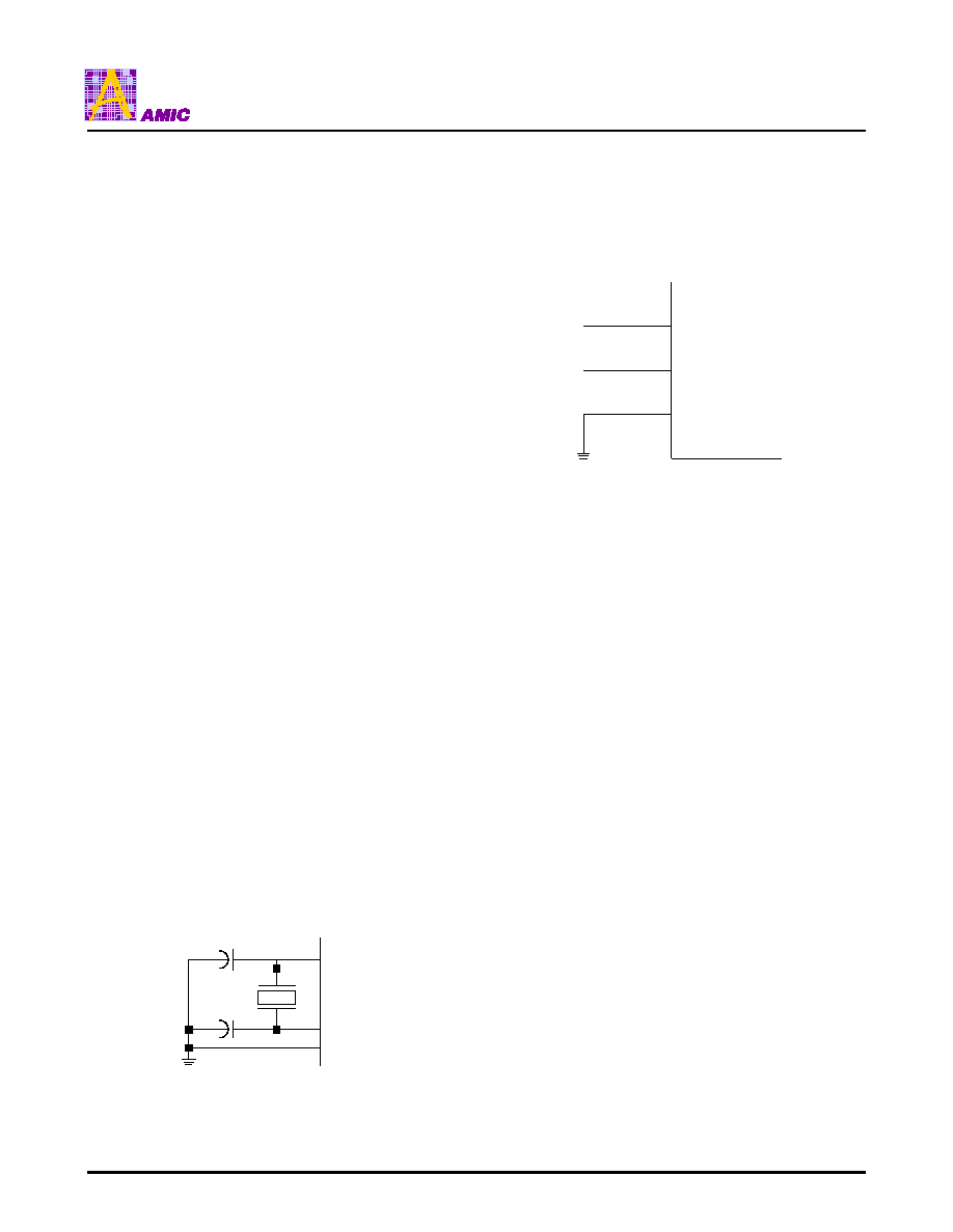
XTAL 2
XTAL 1
V
SS
C1
C2
C1,C2 = 30pF ± 10pF for Crystals
Figure 1. Oscillator Connections
XTAL 2
XTAL 1
V
SS
N/C
EXTERNAL
OSCILLATOR
SIGNAL
Figure 2. External Clock Drive configuration
Functional Description
The A8032 is a high speed 8-bit microcontroller. The architecture consists of a core controller, four general purposes I/O
ports, 256 bytes RAM internal register and a serial port.
This microcontroller supports 111 opcodes and executes instructions in a 6-clock bus cycle. It can reference both a 64K
program address space and a 64K data storage space.
Timer/Counter 0, 1 and 2
Timer 0,1 and 2 each consist of two 8-bit data registers.
These are called TL0 and TH0 for Timer 0. TL1 and TH1
for Timer 1, and TL2 and TH2 for Timer 2. The TMOD
and TCON registers support control function for Timer 0
and Timer 1. The T2CON register provides control
function for Timer 2. When operating reload/capture
mode, RCAP2H and RCAP2L will be used.
Interrupt
The A8032 provides 6 interrupt modes. These consist of
2 external interrupts, 3 internal interrupts and a serial
port interrupt.
The enable/disable interrupt is controlled by IE register in
SFR.
The priority of interrupts is controlled by IP register in
SFR.
Serial Port Transfer
The A8032 provides a full duplex serial transfer function.
This function is controlled by SCON register in SFR.
And the data is storaged in SBUF register during
transmitting and receiving.
Oscillator Characteristics
The oscillator connections are shown as Figure 1. And
Figure 2. When quartz crystal is used, C1 and C2 are
30pF shown in Figure 1. When external clock is used,
the internal clock will be gotten through a divide-by-two
flip-flop. When starting up, the input loading for XTAL1
pin is 100pF. This is due to interaction between the
amplifier and its feedback capacitance interaction. After
the external signal meets the V
IL
and V
IH
specification
the capacitance will not exceed 20pF.
RESET
The external reset signal must be held high for at least
two machine cycles during the oscillator running.
After reset, the ports are held high, SP register to 07H,
all of the other SFR registers except SBUF to 00H, and
SBUF is not reset.
A8032 Series
PRELIMINARY (November,
1998, Version 0.0)
5
AMIC Technology, Inc.
Recommended DC Operating Conditions
(T
A
= -25
°
C to + 85
°
C)
Symbol
Parameter
Min.
Typ.
Max.
Unit
VCC
Supply Voltage
4.5
5.0
5.5
V
GND
Ground
0
0
0
V
V
IH
*
Input High Voltage
2.4
-
VCC+0.2
V
V
IL
Input Low Voltage
0
-
0.8
V
* XTAL1 is a CMOS input. RESET is a Schmit trigger input.
The min. of V
IH
is 3.5 Volts for these two pins.
Absolute Maximum Ratings*
VCC to GND . . . . . . . . . . . . . . . . . . . . . 0.3V to +7.0V
IN, IN/OUT Volt to GND . . . . . . . . . -0.5V to VCC + 0.5V
Operating Temperature, Topr
. . . . . . . -25
°
C to + 85
°
C
Storage Temperature, Tstg . . . . . . . . . -55
°
C to + 125
°
C
Power Dissipation
1*
, Pr . . . . . . . . . . . . . . . . . . . . . . 1W
Soldering Temperature & Time . . . . . . . . . 260
°
C, 10sec
1* : Operating frequency is 40MH
Z
*Comments
Stresses above those listed under "Absolute Maximum
Ratings" may cause permanent damage to this device.
These are stress ratings only. Functional operation of
this device at these or any other conditions above those
indicated in the operational sections of this specification
is not implied or intended. Exposure to the absolute
maximum rating conditions for extended periods may
affect device reliability.
DC Electrical Characteristics (T
A
= -25
°
C to + 85
°
C, VCC = 5V
±
10%)
Symbol
Parameter
Min.
Max.
Unit
Conditions
I
LI
1
Input Leakage Current
-
10
µ
A
V
IN
= GND to VCC
I
LO
Output Leakage Current
-
10
µ
A
V
I/O
= GND to VCC
I
CC
Operating Current
-
50
mA
foper = 40MH
Z
External oscillator is on
XTAL1 pin
No load
V
OL1
Output Low Voltage
(PORT1, PORT2 and PORT3)
-
0.45
V
I
OL
= 2mA
V
OL2
Output Low Voltage
(ALE,
PSEN
and PORT0)
-
0.45
V
I
OL
= 4mA
V
OH1
Output High Voltage
(PORT1, PORT2 and PORT3)
2.4
-
V
I
OH
= -100
µ
A
V
OH2
Output High Voltage
(ALE,
PSEN
and PORT0)
2.4
-
V
I
OH
= -400
µ
A
C
1
Input Pin Capacitance
-
10
pF
1MH
Z
, 25
°
C
1. For RESET pin, the
I
LI
max. is 300
µ
A, since it has an internal pull-low of approx. 30K
resistor.
A8032 Series
PRELIMINARY (November,
1998, Version 0.0)
6
AMIC Technology, Inc.
AC Characteristics (T
A
= -25
°
C to + 85
°
C, VCC = 5V
±
10%)
Symbol
Parameter
Min.
Max.
Unit
Program Memory Cycle
t
AP
ALE Pulse Width
2t
ck
20
1
-
ns
t
ALS
Address Valid to ALE Low
1t
ck
-
ns
t
ALH
Address Hold from ALE Low
1t
ck
-
ns
t
op
PSEN
Pulse Width
3t
ck
- 20
1
-
ns
t
AO
ALE Low to
PSEN
Low
1t
ck
-
ns
t
OI
2
PSEN
Low to Valid Instruction in
-
2t
ck
ns
t
IDO
Input Instruction Hold after
PSEN
High
-
1t
ck
ns
t
IFO
Input Instruction Float after
PSEN
High
-
1t
ck
ns
External Clock
f
OPER
Clock Frequency
0
40
MH
Z
t
CK
3
Clock Period
25
-
ns
t
CKH
4
Clock High Time
10
-
ns
t
CKL
4
Clock Low Time
10
-
ns
Data Memory Cycle
t
PR
RD
Pulse Width
6t
ck
- 20
1
-
ns
t
PD
RD
Low to Valid Data in
-
4t
ck
ns
t
DHR
Data Hold from
RD
High
0
2t
ck
ns
t
DFR
Data Float from
RD
High
0
2t
ck
ns
t
AR
ALE Low to
RD
Low
3t
ck
3t
ck
+ 20
1
ns
t
WP
WR
Pulse Width
6t
ck
- 20
1
-
ns
t
DS
Valid Data to
WR
Low
1t
ck
-
ns
t
DHW
Data Hold from
WR
High
1t
ck
-
ns
t
AW
ALE Low to
WR
Low
3t
ck
3t
ck
+ 20
1
ns
Serial Port Cycle
t
SCK
Serial Port Clock
12t
ck
-
ns
t
KI
Clock Rising Edge to Valid Input Data
-
11t
ck
ns
t
IKH
Input Data to Serial Clock Rising Clock Hold Time
0
-
ns
t
OKS
Output Data to Serial Clock Rising Edge Setup Time
11t
ck
-
ns
t
OKH
Output Data to Serial Clock Rising Edge Hold Time
1t
ck
-
ns
1. This 20 ns is due to buffer driving delay and wire loading.
2. Instruction cycle time is 12 t
ck.
3. tck = 1/ f
oper
4. There are no duty cycle requirements on the XTAL1 input.
A8032 Series
PRELIMINARY (November,
1998, Version 0.0)
7
AMIC Technology, Inc.
Timing Waveforms
Program Memory Cycle
Clock Input Waveform
t
AP
S1
S2
S3
S4
S5
S6
S1
XTAL 1
ALE
t
AO
PSEN
PORT 2
A8 - A15
A8 - A15
t
OP
t
ALS
A0 - A7
A0 - A7
PORT 0
t
ALH
t
OI
t
IHO
t
IFO
INSTRUCTION IN
INSTRUCTION IN
XTAL 1
t
CKH
t
CKL
t
CK
A8032 Series
PRELIMINARY (November,
1998, Version 0.0)
8
AMIC Technology, Inc.
Timing Waveforms (continued)
Data Memory Read Cycle
Data Memory Write Cycle
Serial Port Timing Shift Register Mode
t
DHR
A0-A7
S4
S5
S6
S1
S2
S3
S4
XTAL 1
S5
S6
ALE
PSEN
PORT 2
A8-A15
DATA IN
A0-A7
PORT 0
RD
t
AR
t
RD
t
DFR
t
RP
t
DS
t
DHW
A0-A7
S4
S5
S6
S1
S2
S3
S4
XTAL 1
S5
S6
ALE
PSEN
PORT 2
A8-A15
PORT 0
t
WP
DATA OUT
t
AW
WR
0
1
2
3
4
5
6
7
8
INSTRUCTION
t
SCK
t
OKS
t
OKH
t
KI
t
IKH
VALID
VALID
VALID
VALID
VALID
VALID
VALID
VALID
0
1
2
3
4
5
6
7
SET TI
SET RI
ALE
CLOCK
OUTPUT DATA
INPUT DATA
A8032 Series
PRELIMINARY (November,
1998, Version 0.0)
9
AMIC Technology, Inc.
Ordering Information
Part No.
RAM
FREQ (MH
Z
)
Package
A8032-12
256 Byte
12
40L P-DIP
A8032L-12
256 Byte
12
44L PLCC
A8032-24
256 Byte
24
40L P-DIP
A8032L-24
256 Byte
24
44L PLCC
A8032-40
256 Byte
40
40L P-DIP
A8032L-40
256 Byte
40
44L PLCC
A8032 Series
PRELIMINARY (November,
1998, Version 0.0)
10
AMIC Technology, Inc.
Package Information
P-DIP 40L Outline Dimensions
unit: inches/mm
Dimensions in inches
Dimensions in mm
Symbol
Min
Nom
Max
Min
Nom
Max
A
-
-
0.210
-
-
5.344
A
1
0.015
-
-
0.381
-
-
A
2
0.150
0.155
0.160
3.810
3.937
4.064
B
0.018 TYP
0.457 TYP
B
1
0.050 TYP
1.270 TYP
C
-
0.010
-
-
0.254
-
D
2.049
2.054
2.059
52.045
52.172
52.299
E
0.590
0.600
0.610
14.986
15.240
15.494
E
1
0.542
0.547
0.552
13.767
13.894
14.021
e
1
0.100 TYP
2.540 TYP
L
0.120
0.130
0.140
3.048
3.302
3.556
e
A
0.622
0.642
0.662
15.799
16.307
16.815
Notes:
1. The maximum value of dimension D includes end flash.
2. Dimension E
1
does not include resin fins.
1
40
E
1
A
2
A
L
E
e
A
D
C
0
º/15º
20
21
B
1
B
A
1
Base Plane
Seating Plane
e
1
A8032 Series
PRELIMINARY (November,
1998, Version 0.0)
11
AMIC Technology, Inc.
Package Information
PLCC 44L Outline Dimension
unit: inches/mm
Dimensions in inches
Dimensions in mm
Symbol
Min
Nom
Max
Min
Nom
Max
A
-
-
0.185
-
-
4.70
D
0.648
0.653
0.658
16.46
16.59
16.71
E
0.648
0.653
0.658
16.46
16.59
16.71
H
D
0.680
0.690
0.700
17.27
17.53
17.78
H
E
0.680
0.690
0.700
17.27
17.53
17.78
L
0.090
0.100
0.110
2.29
2.54
2.79
0
°
-
10
°
0
°
-
10
°
Notes:
1. Dimensions D and E do not include resin fins.
2. Dimensions G
D
& G
E
are for PC Board surface mount pad pitch
design reference only.
H
D
D
7
17
18
28
29
39
1
6
E
H
E
44
40
A
1
A
2
A
e
G
D
Seating Plane
b
1
b
0.150 REF
0.020 MIN
L
0.630/0.590
0.050 REF
0.022/0.016
0.032/0.026
G
E
C
0.630/0.590
0.014/0.0008
D
0.004
y