 | –≠–ª–µ–∫—Ç—Ä–æ–Ω–Ω—ã–π –∫–æ–º–ø–æ–Ω–µ–Ω—Ç: Am5X86 | –°–∫–∞—á–∞—Ç—å:  PDF PDF  ZIP ZIP |
This document contains information on a product under development at Advanced Micro Devices. The information is
intended to help you evaluate this product. AMD reserves the right to change or discontinue work on this proposed
product without notice.
Advanced
Micro
Devices
DISTINCTIVE CHARACTERISTICS
s
High-Performance Design
-- Industry-standard write-back cache support
-- Frequent instructions execute in one clock
-- 105.6-million bytes/second burst bus at 33 MHz
-- Flexible write-through and write-back address
control
-- Advanced 0.35-
µ
CMOS-process technology
-- Dynamic bus sizing for 8-, 16-, and 32-bit buses
-- Supports "soft reset" capability
s
High On-Chip Integration
-- 16-Kbyte unified code and data cache
-- Floating-point unit
-- Paged, virtual memory management
s
Enhanced System and Power Management
-- Stop clock control for reduced power
consumption
-- Industry-standard two-pin System Management
Interrupt (SMI) for power management indepen-
dent of processor operating mode and operating
system
-- Static design with Auto Halt power-down support
-- Wide range of chipsets supporting SMM avail-
able to allow product differentiation
s
Complete 32-Bit Architecture
-- Address and data buses
-- All registers
-- 8-, 16-, and 32-bit data types
s
Standard Features
-- 3-V core with 5-V tolerant I/O
-- Available in a 133-MHz version
-- Binary compatible with all Am486
Æ
DX,
Am486DX2, and Am486DX4 microprocessors
-- Wide range of chipsets and support available
through the AMD FusionPC
SM
Program
s
168-pin PGA package or 208-pin SQFP package
s
IEEE 1149.1 JTAG Boundary-Scan Compatibility
s
Supports Environmental Protection Agency's
Energy Star program
-- 3-V operation reduces power consumption up to
40%
-- Energy management capability provides excel-
lent base for energy-efficient design
-- Works with a variety of energy-efficient, power-
managed devices
GENERAL DESCRIPTION
The Am5
X
86TM microprocessor is an addition to the AMD
microprocessor product family. The new processor en-
hances system performance by raising the microproces-
sor operating frequency to the highest levels allowed by
current manufacturing technology, while maintaining
complete compatibility with the standard Am486 proces-
sor architecture and Microsoft
Æ
Windows
Æ
. The CPUs
incorporate write-back cache, flexible clock control, and
enhanced SMM. Table 1 shows available processors
in the Am5
X
86 microprocessor family.
The Am5
X
86 microprocessor family allows write-back
configuration through software and cacheable access
control. On-chip cache lines are configurable as either
write-through or write-back. The CPU clock control fea-
ture permits the CPU clock to be stopped under con-
trolled conditions, allowing reduced power consumption
during system inactivity. The SMM function is implement-
ed with an industry standard two-pin interface.
Table 1. Clocking Options
Operating
Frequency
Input Clock
Available Package
133 MHz
33 MHz
168-pin PGA
133 MHz
33 MHz
208-pin SQFP
PRELIMINARY
Am5
X
86TM
Microprocessor Family
Publication # 19751 Rev: C Amendment/0
Issue Date: March 1996

2
Am5
X
86 Microprocessor
AMD
PRELIMINARY
BLOCK DIAGRAM

AMD
PRELIMINARY
Am5
X
86 Microprocessor
3
ORDERING INFORMATION
Standard Products
AMD standard products are available in several packages and operating ranges. The order number (Valid Combination) is
formed by a combination of the elements below.
A
AMD-X5
Package Type
Family/Core
Valid Combinations
Valid Combinations list configura-
tions planned to be supported in vol-
ume for this device. Consult the local
AMD sales office to confirm avail-
ability of specific valid combinations
and to check on newly released
combinations.
A =168-pin PGA
S = 208-pin SQFP
AMD-X5
Case Temperature
D
W= 55∞ C
Z = 85∞ C
≠ 133
Clock Speed
133 = 133 MHz
W
Operating Voltage
D = 3.45 V
F = 3.3 V
Valid Combinations
OPN
Package Type
Operating Voltage
Case Temperature
(Max)
AMD-X5-133ADW
PGA
3.45 V
55∞ C
AMD-X5-133ADZ
PGA
3.45 V
85∞ C
AMD-X5-133SFZ
SQFP
3.3 V
85∞ C
AMD-X5-133SDZ
SQFP
3.45 V
85∞ C

4
Am5
X
86 Microprocessor
AMD
PRELIMINARY
Table of Contents
1
Connection Diagrams and Pin Designations ......................................................................................... 8
1.1 168-Pin PGA (Pin Grid Array) Package .......................................................................................... 8
1.2 168-Pin PGA Designations (Functional Grouping) ......................................................................... 9
1.3 208-Pin SQFP (Shrink Quad Flat Pack) Package ........................................................................ 10
1.4 208-Pin SQFP Designations (Functional Grouping) ..................................................................... 11
2
Logic Symbol ...................................................................................................................................... 12
3
Pin Description .................................................................................................................................... 13
4
Functional Description ........................................................................................................................ 18
4.1 Overview ....................................................................................................................................... 18
4.2 Memory ......................................................................................................................................... 18
4.3 Modes of Operation ...................................................................................................................... 18
4.3.1 Real mode ........................................................................................................................... 18
4.3.2 Virtual mode ........................................................................................................................ 18
4.3.3 Protected mode ................................................................................................................... 18
4.3.4 System Management mode ................................................................................................ 18
4.4 Cache Architecture ....................................................................................................................... 18
4.4.1 Write-Through Cache .......................................................................................................... 18
4.4.2 Write-Back Cache ............................................................................................................... 18
4.5 Write-Back Cache Protocol ........................................................................................................... 19
4.5.1 Cache Line Overview .......................................................................................................... 19
4.5.2 Line Status and Line State .................................................................................................. 19
4.5.2.1 Invalid ......................................................................................................................... 19
4.5.2.2 Exclusive .................................................................................................................... 19
4.5.2.3 Shared ....................................................................................................................... 19
4.5.2.4 Modified ..................................................................................................................... 19
4.6 Cache Replacement Description .................................................................................................. 20
4.7 Memory Configuration ................................................................................................................... 20
4.7.1 Cacheability ......................................................................................................................... 20
4.7.2 Write-Through/Write-Back ................................................................................................... 20
4.8 Cache Functionality in Write-Back mode ...................................................................................... 20
4.8.1 Processor-Initiated Cache Functions and State Transitions ............................................... 20
4.8.2 Snooping Actions and State Transitions ............................................................................. 21
4.8.2.1 Difference between Snooping Access Cases ............................................................ 21
4.8.2.2 HOLD Bus Arbitration Implementation ....................................................................... 22
4.8.2.2.1 Processor-Induced Bus Cycles ........................................................................ 22
4.8.2.2.2 External Read ................................................................................................... 22
4.8.2.2.3 External Write ................................................................................................... 22
4.8.2.2.4 HOLD/HLDA External Access TIming .............................................................. 22
4.8.3 External Bus Master Snooping Actions ............................................................................... 25
4.8.3.1 Snoop Miss ................................................................................................................. 25
4.8.3.2 Snoop Hit to a Non-Modified Line .............................................................................. 25
4.8.4 Write-Back Case ................................................................................................................. 25
4.8.5 Write-Back and Pending Access ......................................................................................... 26
4.8.5.1 HOLD/HLDA Write-Back Design Considerations ....................................................... 27
4.8.5.2 AHOLD Bus Arbitration Implementation .................................................................... 28
4.8.5.3 Normal Write-Back ..................................................................................................... 28
4.8.6 Reordering of Write-Backs (AHOLD) with BOFF ................................................................. 29
4.8.7 Special Scenarios For AHOLD Snooping ............................................................................ 30
4.8.7.1 Write Cycle Reordering due to Buffering ................................................................... 30
4.8.7.2 BOFF Write-Back Arbitration Implementation ............................................................ 32
4.8.8 BOFF Design Considerations .............................................................................................. 32
4.8.8.1 Cache Line Fills ......................................................................................................... 32
4.8.8.2 Cache Line Copy-Backs ............................................................................................ 32
4.8.8.3 Locked Accesses ....................................................................................................... 32

AMD
PRELIMINARY
Am5
X
86 Microprocessor
5
4.8.9 BOFF During Write-Back ..................................................................................................... 32
4.8.10 Snooping Characteristics During a Cache Line Fill ........................................................... 32
4.8.11 Snooping Characteristics During a Copy-Back ................................................................. 32
4.9 Cache Invalidation and Flushing in Write-Back mode .................................................................. 33
4.9.1 Cache Invalidation through Software .................................................................................. 33
4.9.2 Cache Invalidation through Hardware ................................................................................. 33
4.9.3 Snooping During Cache Flushing ........................................................................................ 34
4.10 Burst Write .................................................................................................................................. 34
4.10.1 Locked Accesses .............................................................................................................. 35
4.10.2 Serialization ....................................................................................................................... 35
4.10.3 PLOCK Operation in Write-Through mode ........................................................................ 36
5
Clock Control ...................................................................................................................................... 36
5.1 Clock Generation .......................................................................................................................... 36
5.2 Stop Clock ..................................................................................................................................... 36
5.2.1 External Interrupts in Order of Priority ................................................................................. 36
5.3 Stop Grant Bus Cycle ................................................................................................................... 36
5.4 Pin State during Stop Grant .......................................................................................................... 37
5.5 Clock Control State Diagram ........................................................................................................ 37
5.5.1 Normal State ........................................................................................................................ 37
5.5.2 Stop Grant State .................................................................................................................. 37
5.5.3 Stop Clock State .................................................................................................................. 39
5.5.4 Auto Halt Power Down State ............................................................................................... 39
5.5.5 Stop Clock Snoop State (Cache Invalidations) .................................................................... 39
5.5.6 Cache Flush State ............................................................................................................... 39
6
SRESET Function ............................................................................................................................... 39
7
System Management mode ................................................................................................................ 39
7.1 Overview ....................................................................................................................................... 39
7.2 Terminology .................................................................................................................................. 40
7.3 System Management Interrupt Processing ................................................................................... 40
7.3.1 System Management Interrupt Processing ......................................................................... 41
7.3.2 SMI Active (SMIACT) .......................................................................................................... 41
7.3.3 SMRAM ............................................................................................................................... 42
7.3.4 SMRAM State Save Map .................................................................................................... 43
7.4 Entering System Management mode ............................................................................................ 44
7.5 Exiting System Management mode .............................................................................................. 44
7.6 Processor Environment ................................................................................................................. 44
7.7 Executing System Management mode Handler ............................................................................ 45
7.7.1 Exceptions and Interrupts with System Management mode ............................................... 46
7.7.2 SMM Revisions Identifier ..................................................................................................... 46
7.7.3 Auto HALT Restart .............................................................................................................. 47
7.7.4 I/O Trap Restart ................................................................................................................... 47
7.7.5 I/O Trap Word ...................................................................................................................... 47
7.7.6 SMM Base Relocation ......................................................................................................... 48
7.8 SMM System Design Considerations ........................................................................................... 48
7.8.1 SMRAM Interface ................................................................................................................ 48
7.8.2 Cache Flushes .................................................................................................................... 49
7.8.3 A20M Pin ............................................................................................................................. 49
7.8.4 CPU Reset during SMM ...................................................................................................... 52
7.8.5 SMM and Second Level Write Buffers ................................................................................ 52
7.8.6 Nested SMI and I/O Restart ................................................................................................ 52
7.9 SMM Software Considerations ..................................................................................................... 52
7.9.1 SMM Code Considerations ................................................................................................. 52
7.9.2 Exception Handling ............................................................................................................. 52
7.9.3 Halt during SMM .................................................................................................................. 53
7.9.4 Relocating SMRAM to an Address above 1 Mbyte ............................................................. 53

6
Am5
X
86 Microprocessor
AMD
PRELIMINARY
8
Test Registers 4 and 5 Modifications .................................................................................................. 53
8.1 TR4 Definition ................................................................................................................................ 53
8.2 TR5 Definition ................................................................................................................................ 54
8.3 Using TR4 and TR5 for Cache Testing.......................................................................................... 55
8.3.1 Example 1: Reading the Cache (Write-back mode only) ..................................................... 55
8.3.2 Example 2: Writing the Cache .............................................................................................. 55
8.3.3 Example 3: Flushing the Cache ........................................................................................... 55
9
Am5
X
86 CPU Functional Differences ................................................................................................. 55
9.1 Status after Reset ......................................................................................................................... 55
9.2 Cache Status ................................................................................................................................ 55
9.3 CLKMUL Pin ................................................................................................................................. 55
10 Am5
X
86 CPU Identification ................................................................................................................. 56
10.1 DX Register at RESET ................................................................................................................ 56
10.2 CPUID Instruction ....................................................................................................................... 56
10.2.1 CPUID Timing ................................................................................................................... 56
10.2.2 CPUID Operation .............................................................................................................. 56
11 Electrical Data ..................................................................................................................................... 57
11.1 Power and Grounding ................................................................................................................. 57
11.1.1 Power Connections ........................................................................................................... 57
11.1.2 Power Decoupling Recommendations .............................................................................. 57
11.1.3 Other Connection Recommendations ............................................................................... 57
12 Package Thermal Specifications ......................................................................................................... 65
13 Physical Dimensions ........................................................................................................................... 66
LIST OF FIGURES
Figure 1
Processor-Induced Line Transitions in Write-Back mode ....................................................... 20
Figure 2
Snooping State Transitions ..................................................................................................... 21
Figure 3
Typical System Block Diagram for HOLD/HLDA Bus Arbitration ............................................ 22
Figure 4
External Read ......................................................................................................................... 23
Figure 5
External Write .......................................................................................................................... 23
Figure 6
Snoop of On-Chip Cache That Does Not Hit a Line ................................................................ 24
Figure 7
Snoop of On-Chip Cache That Hits a Non-modified Line ........................................................ 24
Figure 8
Snoop That Hits a Modified Line (Write-Back) ........................................................................ 25
Figure 9
Write-Back and Pending Access ............................................................................................. 26
Figure 10 Valid HOLD Assertion During Write-Back ............................................................................... 27
Figure 11 Closely Coupled Cache Block Diagram .................................................................................. 28
Figure 12 Snoop Hit Cycle with Write-Back ............................................................................................. 29
Figure 13 Cycle Reordering with BOFF (Write-Back) .............................................................................. 30
Figure 14 Write Cycle Reordering Due to Buffering ................................................................................ 31
Figure 15 Latest Snooping of Copy-Back ................................................................................................ 33
Figure 16 Burst Write .............................................................................................................................. 34
Figure 17 Burst Read with BOFF Assertion ............................................................................................ 34
Figure 18 Burst Write with BOFF Assertion ............................................................................................. 35
Figure 19 Entering Stop Grant State ....................................................................................................... 37
Figure 20 Stop Clock State Machine ....................................................................................................... 38
Figure 21 Recognition of Inputs when Exiting Stop Grant State ............................................................. 38
Figure 22 Basic SMI Interrupt Service ..................................................................................................... 40
Figure 23 Basic SMI Hardware Interface.................................................................................................. 41
Figure 24 SMI Timing for Servicing an I/O Trap ...................................................................................... 41
Figure 25 SMIACT Timing ....................................................................................................................... 42
Figure 26 Redirecting System Memory Address to SMRAM ................................................................... 42
Figure 27 Transition to and from SMM .................................................................................................... 44
Figure 28 Auto HALT Restart Register Offset .......................................................................................... 47
Figure 29 I/O Instruction Restart Register Offset .................................................................................... 47

AMD
PRELIMINARY
Am5
X
86 Microprocessor
7
Figure 30 SMM Base Slot Offset ............................................................................................................. 48
Figure 31 SRAM Usage .......................................................................................................................... 48
Figure 32 SMRAM Location .................................................................................................................... 49
Figure 33 SMM Timing in Systems Using Non-Overlaid Memory Space and Write-Through Mode
with Caching Enabled During SMM.......................................................................................... 50
Figure 34 SMM Timing in Systems Using Non-Overlaid Memory Spaces and Write-Back Mode with
Caching Enabled During SMM ................................................................................................. 50
Figure 35 SMM Timing in Systems Using Non-Overlaid Memory Spaces and Write-Back Mode with
Caching Disabled During SMM ................................................................................................ 50
Figure 36 SMM Timing in Systems Using Overlaid Memory Space and Write-Through Mode with
Caching Enabled During SMM ................................................................................................. 51
Figure 37 SMM Timing in Systems Using Overlaid Memory Spaces and Write-Through Mode with
Caching Disabled During SMM ................................................................................................ 51
Figure 38 SMM Timing in Systems Using Overlaid Memory Spaces and Configured in
Write-Back Mode...................................................................................................................... 51
Figure 39 CLK Waveforms ...................................................................................................................... 61
Figure 40 Output Valid Delay Timing ...................................................................................................... 61
Figure 41 Maximum Float Delay Timing .................................................................................................. 62
Figure 42 PCHK Valid Delay Timing ....................................................................................................... 62
Figure 43 Input Setup and Hold Timing ................................................................................................... 63
Figure 44 RDY and BRDY Input Setup and Hold Timing ........................................................................ 63
Figure 45 TCK Waveforms ...................................................................................................................... 64
Figure 46 Test Signal Timing Diagram .................................................................................................... 64
LIST OF TABLES
Table 1
Clocking Options ....................................................................................................................... 1
Table 2
EADS Sample Time ................................................................................................................ 14
Table 3
Cache Line Organization ......................................................................................................... 19
Table 4
Legal Cache Line States ......................................................................................................... 19
Table 5
MESI Cache Line Status ......................................................................................................... 20
Table 6
Key to Switching Waveforms ................................................................................................... 22
Table 7
WBINVD/INVD Special Bus Cycles ......................................................................................... 33
Table 8
FLUSH Special Bus Cycles ..................................................................................................... 34
Table 9
Pin State during Stop Grant Bus State .................................................................................... 37
Table 10
SMRAM State Save Map ........................................................................................................ 43
Table 11
SMM Initial CPU Core Register Settings ................................................................................. 45
Table 12
Segment Register Initial States ............................................................................................... 45
Table 13
SMM Revision Identifier .......................................................................................................... 46
Table 14
SMM Revision Identifier Bit Definitions ................................................................................... 46
Table 15
HALT Auto Restart Configuration ............................................................................................ 47
Table 16
I/O Trap Word Configuration ................................................................................................... 47
Table 17
Test Register TR4 Bit Descriptions ......................................................................................... 53
Table 18
Test Register TR5 Bit Descriptions ......................................................................................... 53
Table 19
CPU ID Codes ......................................................................................................................... 56
Table 20
CPUID Instruction Description ................................................................................................. 56
Table 21
Thermal Resistance (∞C/W)
JC
and
JA
for the Am5
X
86 CPU in 168-Pin PGA Package ....... 65
Table 22
Maximum T
A
at Various Airflows in ∞C .................................................................................... 65
Table 23
Maximum T
A
for SQFP Package by Clock Frequency ............................................................. 65

8
Am5
X
86 Microprocessor
AMD
PRELIMINARY
1
CONNECTION DIAGRAMS AND PIN DESIGNATIONS
1.1
168-pin PGA (Pin Grid Array) Package
A
B
C
D
E
F
G
H
J
K
L
M
N
P
Q
R
S
A
B
C
D
E
F
G
H
J
K
L
M
N
P
Q
R
S
1
2
3
4
5
6
7
8
9
10
11
12
13
14
15
16
17
1
2
3
4
5
6
7
8
9
10
11
12
13
14
15
16
17
D20
D19
D11
D9
V
SS
DP1
V
SS
V
SS
INC
V
SS
V
SS
V
SS
D2
D0
A31
A28
A27
D22
D21
D18
D13
V
CC
D8
V
CC
D3
D5
V
CC
D6
V
CC
D1
A29
V
SS
A25
A26
TCK
V
SS
CLK
D17
D10
D15
D12
DP2
D16
D14
D7
D4
DP0
A30
A17
V
CC
A23
D23
V
SS
V
CC
A19
V
SS
VOLDET
DP3
V
SS
V
CC
D13
VCC
D8
VCC
D3
D5
VCC
D6
VCC
D1
A29
A21
A18
A14
D24
D25
D27
D13
VCC
D8
VCC
D3
D5
VCC
D6
VCC
D1
A29
A24
V
CC
V
SS
V
SS
V
CC
D26
D13
VCC
D8
VCC
D3
D5
VCC
D6
VCC
D1
A29
A22
A15
A12
D29
D31
D28
D13
VCC
D8
VCC
D3
D5
VCC
D6
VCC
D1
A29
A20
V
CC
V
SS
V
SS
V
CC
D30
D13
VCC
D8
VCC
D3
D5
VCC
D6
VCC
D1
A29
A16
V
CC
V
SS
TDI
TMS
FERR
A2
V
CC
V
SS
INV
SMI SRESET
VCC
D8
VCC
D3
D5
VCC
D6
VCC
D1
A29
A13
V
CC
V
SS
V
SS
V
CC
UP
D13
VCC
D8
VCC
D3
D5
VCC
D6
VCC
D1
A29
A9
V
CC
V
SS
HITM CACHE SMIACT
A5
A11
V
SS
INC
WB/WT INC
A7
A8
A10
IGNNE
NMI FLUSH A20M HOLD KEN STPCLK BRDY BE2
BE0
PWT
D/C
LOCK HLDA BREQ
A3
A6
INTR
TDO RESET BS8
V
CC
RDY
V
CC
V
CC
BE1
V
CC
V
CC
V
CC
M/IO
V
CC
PLOCK BLAST A4
AHOLD EADS
BS16 BOFF
V
SS
BE3
V
SS
V
SS
PCD
V
SS
V
SS
V
SS
W/R
V
SS
PCHK CLKMUL ADS
PIN SIDE VIEW

Am5
X
86 Microprocessor
9
AMD
PRELIMINARY
1.2
168-pin PGA Designations (Functional Grouping)
Address
Data
Control
Test
INC
V
cc
V
ss
Pin
Name
Pin
No.
Pin
Name
Pin
No.
Pin
Name
Pin
No.
Pin
Name
Pin
No.
Pin
No.
Pin
No.
Pin
No.
A2
A3
A4
A5
A6
A7
A8
A9
A10
A11
A12
A13
A14
A15
A16
A17
A18
A19
A20
A21
A22
A23
A24
A25
A26
A27
A28
A29
A30
A31
Q-14
R-15
S-16
Q-12
S-15
Q-13
R-13
Q-11
S-13
R-12
S-7
Q-10
S-5
R-7
Q-9
Q-3
R-5
Q-4
Q-8
Q-5
Q-7
S-3
Q-6
R-2
S-2
S-1
R-1
P-2
P-3
Q-1
D0
D1
D2
D3
D4
D5
D6
D7
D8
D9
D10
D11
D12
D13
D14
D15
D16
D17
D18
D19
D20
D21
D22
D23
D24
D25
D26
D27
D28
D29
D30
D31
P-1
N-2
N-1
H-2
M-3
J-2
L-2
L-3
F-2
D-1
E-3
C-1
G-3
D-2
K-3
F-3
J-3
D-3
C-2
B-1
A-1
B-2
A-2
A-4
A-6
B-6
C-7
C-6
C-8
A-8
C-9
B-8
A20M
ADS
AHOLD
BE0
BE1
BE2
BE3
BLAST
BOFF
BRDY
BREQ
BS8
BS16
CACHE
CLK
CLKMUL
D/C
DP0
DP1
DP2
DP3
EADS
FERR
FLUSH
HITM
HLDA
HOLD
IGNNE
INTR
INV
KEN
LOCK
M/IO
NMI
PCD
PCHK
PLOCK
PWT
RDY
RESET
SMI
SMIACT
SRESET
STPCLK
UP
VOLDET
WB/WT
W/R
D-15
S-17
A-17
K-15
J-16
J-15
F-17
R-16
D-17
H-15
Q-15
D-16
C-17
B-12
C-3
R-17
M-15
N-3
F-1
H-3
A-5
B-17
C-14
C-15
A-12
P-15
E-15
A-15
A-16
A-10
F-15
N-15
N-16
B-15
J-17
Q-17
Q-16
L-15
F-16
C-16
B-10
C-12
C-10
G-15
C-11
S-4
B-13
N-17
TCK
TDI
TDO
TMS
A-3
A-14
B-16
B-14
A-13
C-13
J-1
B-7
B-9
B-11
C-4
C-5
E-2
E-16
G-2
G-16
H-16
K-2
K-16
L-16
M-2
M-16
P-16
R-3
R-6
R-8
R-9
R-10
R-11
R-14
A-7
A-9
A-11
B-3
B-4
B-5
E-1
E-17
G-1
G-17
H-1
H-17
K-1
K-17
L-1
L-17
M-1
M-17
P-17
Q-2
R-4
S-6
S-8
S-9
S-10
S-11
S-12
S-14
Notes:
1. VOLDET is connected internally to V
SS
.
2. INC = Internal No Connect

10
Am5
X
86 Microprocessor
AMD
PRELIMINARY
1.3
208-pin SQFP (Shrink Quad Flat Pack) Package
TOP VIEW

Am5
X
86 Microprocessor
11
AMD
PRELIMINARY
1.4
208-pin SQFP Designations (Functional Grouping)
Address
Data
Control
Test
INC
V
cc
V
ss
Pin Name
Pin
No.
Pin Name
Pin
No.
Pin
Name
Pin
No.
Pin
Name
Pin
No.
Pin
No.
Pin
No.
Pin
No.
A2
A3
A4
A5
A6
A7
A8
A9
A10
A11
A12
A13
A14
A15
A16
A17
A18
A19
A20
A21
A22
A23
A24
A25
A26
A27
A28
A29
A30
A31
202
197
196
195
193
192
190
187
186
182
180
178
177
174
173
171
166
165
164
161
160
159
158
154
153
152
151
149
148
147
D0
D1
D2
D3
D4
D5
D6
D7
D8
D9
D10
D11
D12
D13
D14
D15
D16
D17
D18
D19
D20
D21
D22
D23
D24
D25
D26
D27
D28
D29
D30
D31
144
143
142
141
140
130
129
126
124
123
119
118
117
116
113
112
108
103
101
100
99
93
92
91
87
85
84
83
79
78
75
74
A20M
ADS
AHOLD
BE0
BE1
BE2
BE3
BLAST
BOFF
BRDY
BREQ
BS8
BS16
CACHE
CLK
CLKMUL
D/C
DP0
DP1
DP2
DP3
EADS
FERR
FLUSH
HITM
HLDA
HOLD
IGNNE
INTR
INV
KEN
LOCK
M/IO
NMI
PCD
PCHK
PLOCK
PWT
RDY
RESET
SMI
SRESET
STPCLK
SMIACT
UP
WB/WT
W/R
47
203
17
31
32
33
34
204
6
5
30
8
7
70
24
11
39
145
125
109
90
46
66
49
63
26
16
72
50
71
13
207
37
51
41
4
206
40
12
48
65
58
73
59
194
64
27
TCK
TDI
TDO
TMS
18
168
68
167
3
67
96
127
2
9
14
19
20
22
23
25
29
35
38
42
44
45
54
56
60
62
69
77
80
82
86
89
95
98
102
106
111
114
121
128
131
133
134
136
137
139
150
155
162
163
169
172
176
179
183
185
188
191
198
200
205
1
10
15
21
28
36
43
52
53
55
57
61
76
81
88
94
97
104
105
107
110
115
120
122
132
135
138
146
156
157
170
175
181
184
189
199
201
208
Note:
INC = Internal No Connect

12
Am5
X
86 Microprocessor
AMD
PRELIMINARY
2
LOGIC SYMBOL
DP3≠DP0
A31≠A4
CLK
A20M
M/IO
Am5
X
86
CPU
W/R
D/C
28
2
LOCK
4
BE3≠BE0
Clock
Address Bus
Bus Cycle
Definition
Address
PLOCK
BS8
BS16
ADS
RDY
Bus Cycle
Control
32
4
INTR
NMI
RESET
Interrupts
PCHK
A3≠A2
BRDY
BLAST
PWT
PCD
KEN
FLUSH
EADS
AHOLD
Data Parity
Data Bus
Burst
Control
Page
Cacheability
Invalidation
Cache Control/
D31≠D0
TMS
TDI
TDO
TCK
IEEE Test
Port Access
FERR
IGNNE
Numeric Error
Reporting
Bus Arbitration
BREQ
HOLD
HLDA
BOFF
CACHE
CLKMUL
Clock Multiplier
Mask
HITM
INV
SMI
SMIACT
SMM
SRESET
STPCLK
Stop Clock
UP
Upgrade
VOLDET
Voltage Detect
Present
WB/WT

Am5
X
86 Microprocessor
13
AMD
PRELIMINARY
3
PIN DESCRIPTIONS
The Am5
X
86 microprocessor provides the complete in-
terface support offered by the Enhanced Am486 micro-
processor family products. The CLKMUL pin settings
have changed to accommodate the higher operating
speed selection.
A20M
Address Bit 20 Mask (Active Low; Input)
A Low signal on the A20M pin causes the microproces-
sor to mask address line A20 before performing a lookup
to the internal cache, or driving a memory cycle on the
bus. Asserting A20M causes the processor to wrap the
address at 1 Mbyte, emulating Real mode operation.
The signal is asynchronous, but must meet setup and
hold times t
20
and t
21
for recognition during a specific
clock. During normal operation, A20M should be sam-
pled High at the falling edge of RESET.
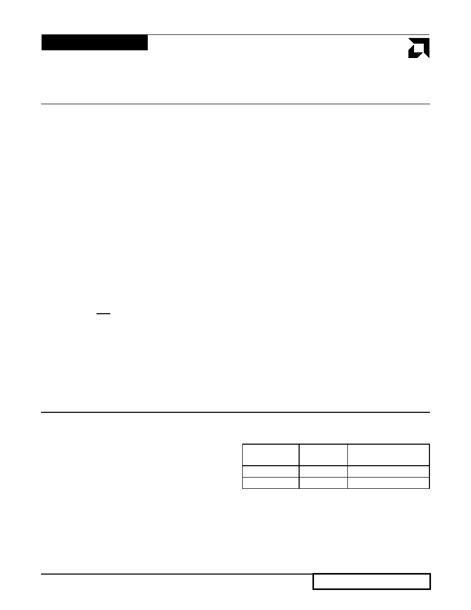
A31≠A4/A3≠A2
Address Lines (Inputs/Outputs)/(Outputs)
Pins A31≠A2 define a physical area in memory or indi-
cate an input/output (I/O) device. Address lines A31≠A4
drive addresses into the microprocessor to perform
cache line invalidations. Input signals must meet setup
and hold times t
22
and t
23
. A31≠A2 are not driven during
bus or address hold.
ADS
Address Status (Active Low; Output)
A Low output from this pin indicates that a valid bus
cycle definition and address are available on the cycle
definition lines and address bus. ADS is driven active by
the same clock as the addresses. ADS is active Low and is
not driven during bus hold.
AHOLD
Address Hold (Active High; Input)
The external system may assert AHOLD to perform a
cache snoop. In response to the assertion of AHOLD,
the microprocessor stops driving the address bus A31≠
A2 in the next clock. The data bus remains active and
data can be transferred for previously issued read or
write bus cycles during address hold. AHOLD is recog-
nized even during RESET and LOCK. The earliest that
AHOLD can be deasserted is two clock cycles after
EADS is asserted to start a cache snoop. If HITM is
activated due to a cache snoop, the microprocessor
completes the current bus activity and then asserts ADS
and drives the address bus while AHOLD is active. This
starts the write-back of the modified line that was the
target of the snoop.
BE3
≠
BE0
Byte Enable (Active Low; Outputs)
The byte enable pins indicate which bytes are enabled
and active during read or write cycles. During the first
cache fill cycle, however, an external system should
ignore these signals and assume that all bytes are
active.
s
BE3 for D31≠D24
s
BE2 for D23≠D16
s
BE1 for D15≠D8
s
BE0 for D7≠D0
BE3≠BE0 are active Low and are not driven during bus
hold.
BLAST
Burst Last (Active Low; Output)
Burst Last goes Low to tell the CPU that the next BRDY
signal completes the burst bus cycle. BLAST is active
for both burst and non-burst cycles. BLAST is active
Low and is not driven during a bus hold.
BOFF
Back Off (Active Low; Input)
This input signal forces the microprocessor to float all
pins normally floated during hold, but HLDA is not as-
serted in response to BOFF. BOFF has higher priority
than RDY or BRDY; if both are returned in the same
clock, BOFF takes effect. The microprocessor remains
in bus hold until BOFF goes High. If a bus cycle is in
progress when BOFF is asserted, the cycle restarts.
BOFF must meet setup and hold times t
18
and t
19
for
proper operation. BOFF has an internal weak pull-up.
BRDY
Burst Ready Input (Active Low; Input)
The BRDY signal performs the same function during a
burst cycle that RDY performs during a non-burst cycle.
BRDY indicates that the external system has presented
valid data in response to a read, or that the external
system has accepted data in response to a write. BRDY
is ignored when the bus is idle and at the end of the first
clock in a bus cycle. BRDY is sampled in the second
and subsequent clocks of a burst cycle. The data pre-
sented on the data bus is strobed into the microproces-
sor when BRDY is sampled active. If RDY is returned
simultaneously with BRDY, BRDY is ignored and the
cycle is converted to a non-burst cycle. BRDY is active
Low and has a small pull-up resistor, and must satisfy
the setup and hold times t
16
and t
17
.
BREQ
Internal Cycle Pending (Active High; Output)
BREQ indicates that the microprocessor has generated
a bus request internally, whether or not the micropro-
cessor is driving the bus. BREQ is active High and is
floated only during Tri-state Test mode (see FLUSH).

14
Am5
X
86 Microprocessor
AMD
PRELIMINARY
BS8/BS16
Bus Size 8 (Active Low; Input)/
Bus Size 16 (Active Low; Input)
The BS8 and BS16 signals allow the processor to op-
erate with 8-bit and 16-bit I/O devices by running multiple
bus cycles to respond to data requests: four for 8-bit
devices, and two for 16-bit devices. The bus sizing pins
are sampled every clock. The microprocessor samples
the pins every clock before RDY to determine the ap-
propriate bus size for the requesting device. The signals
are active Low input with internal pull-up resistors, and
must satisfy setup and hold times t
14
and t
15
for correct
operation. Bus sizing is not permitted during copy-back
or write-back operation. BS8 and BS16 are ignored dur-
ing copy-back or write-back cycles.
CACHE
Internal Cacheability (Active Low; Output)
In Write-through mode, this signal always floats. In
Write-back mode for processor-initiated cycles, a Low
output on this pin indicates that the current read cycle
is cacheable, or that the current cycle is a burst write-
back or copy-back cycle. If the CACHE signal is driven
High during a read, the processor will not cache the data
even if the KEN pin signal is asserted. If the processor
determines that the data is cacheable, CACHE goes
active when ADS is asserted and remains in that state
until the next RDY or BRDY is asserted. CACHE floats
in response to a BOFF or HOLD request.
CLK
Clock (Input)
The CLK input provides the basic microprocessor timing
signal. The CLKMUL input selects the multiplier value
used to generate the internal operating frequency for
the Am5
X
86 microprocessor family. All external timing
parameters are specified with respect to the rising edge
of CLK. The clock signal passes through an internal
Phase-Lock Loop (PLL).
CLKMUL
Clock Multiplier (Input)
The microprocessor samples the CLKMUL input signal
at RESET to determine the design operating frequency.
An internal pull-up resistor connects to V
CC
, which se-
lects Clock-tripled mode if the input is High or left float-
ing. For Clock-quadrupled mode, the input must be
pulled Low. For 133-MHz processors, this input must
always be connected to V
SS
to ensure correct operation.
D31
≠
D0
Data Lines (Inputs/Outputs)
Lines D31≠D0 define the data bus. The signals must
meet setup and hold times t
22
and t
23
for proper read
operations. These pins are driven during the second
and subsequent clocks of write cycles.
D/C
Data/Control (Output)
This bus cycle definition pin distinguishes memory and
I/O data cycles from control cycles. The control cycles
are:
s
Interrupt Acknowledge
s
Halt/Special Cycle
s
Code Read (instruction fetching)
DP3
≠
DP0
Data Parity (Inputs/Outputs)
Data parity is generated on all write data cycles with the
same timing as the data driven by the microprocessor.
Even parity information must be driven back into the
microprocessor on the data parity pins with the same
timing as read information to ensure that the processor
uses the correct parity check. The signals read on these
pins do not affect program execution. Input signals must
meet setup and hold times t
22
and t
23
. DP3≠DP0 should
be connected to V
CC
through a pull-up resistor in sys-
tems not using parity. DP3≠DP0 are active High and are
driven during the second and subsequent clocks of write
cycles.
EADS
External Address Strobe (Active Low; Input)
This signal indicates that a valid external address has
been driven on the address pins A31≠A4 of the micro-
processor to be used for a cache snoop. This signal is
recognized while the processor is in hold (HLDA is driv-
en active), while forced off the bus with the BOFF input,
or while AHOLD is asserted. The microprocessor ig-
nores EADS at all other times. EADS is not recognized
if HITM is active, nor during the clock after ADS, nor
during the clock after a valid assertion of EADS. Snoops
to the on-chip cache must be completed before another
snoop cycle is initiated. Table 2 describes EADS when
first sampled. EADS can be asserted every other clock
cycle as long as the hold remains active and HITM re-
mains inactive. INV is sampled in the same clock period
that EADS is asserted. EADS has an internal weak pull-
up.
Note:
The triggering signal (AHOLD, HOLD, or BOFF) must remain
active for at least 1 clock after EADS to ensure proper oper-
ation.
Table 2. EADS Sample Time
Trigger
EADS First Sampled
AHOLD
Second clock after AHOLD asserted
HOLD
First clock after HLDA asserted
BOFF
Second clock after BOFF asserted

Am5
X
86 Microprocessor
15
AMD
PRELIMINARY
FERR
Floating-Point Error (Active Low; Output)
Driven active when a floating-point error occurs, FERR
is similar to the ERROR pin on a 387 math coprocessor.
FERR is included for compatibility with systems using
DOS-type floating-point error reporting. FERR is active
Low, and is not floated during bus hold, except during
Tri-state Test mode (see FLUSH).
FLUSH
Cache Flush (Active Low; Input)
In Write-back mode, FLUSH forces the microprocessor
to write-back all modified cache lines and invalidate its
internal cache. The microprocessor generates two flush
acknowledge special bus cycles to indicate completion
of the write-back and invalidation. In Write-through
mode, FLUSH invalidates the cache without issuing a
special bus cycle. FLUSH is an active Low input that
needs to be asserted only for one clock. FLUSH is asyn-
chronous, but setup and hold times t
20
and t
21
must be
met for recognition in any specific clock. Sampling
FLUSH Low in the clock before the falling edge of
RESET causes the microprocessor to enter Tri-state
Test mode.
HITM
Hit Modified Line (Active Low; Output)
In Write-back mode (WB/WT=1 at RESET), HITM indi-
cates that an external snoop cache tag comparison hit
a modified line. When a snoop hits a modified line in the
internal cache, the microprocessor asserts HITM two
clocks after EADS is asserted. The HITM signal stays
asserted (Low) until the last BRDY for the corresponding
write-back cycle. At all other times, HITM is deasserted
(High). During RESET, the HITM signal can be used to
detect whether the CPU is operating in Write-back
mode. In Write-back mode (WB/WT=1 at RESET), HITM
is deasserted (driven High) until the first snoop that hits
a modified line. In Write-through mode, HITM floats at
all times.
HLDA
Hold Acknowledge (Active High; Output)
The HLDA signal is activated in response to a hold re-
quest presented on the HOLD pin. HLDA indicates that
the microprocessor has given the bus to another local
bus master. HLDA is driven active in the same clock in
which the microprocessor floats its bus. HLDA is driven
inactive when leaving bus hold. HLDA is active High and
remains driven during bus hold. HLDA is floated only
during Tri-state Test mode (see FLUSH).
HOLD
Bus Hold Request (Active High; Input)
HOLD gives control of the microprocessor bus to anoth-
er bus master. In response to HOLD going active, the
microprocessor floats most of its output and input/output
pins. HLDA is asserted after completing the current bus
cycle, burst cycle, or sequence of locked cycles. The
microprocessor remains in this state until HOLD is deas-
serted. HOLD is active High and does not have an in-
ternal pull-down resistor. HOLD must satisfy setup and
hold times t
18
and t
19
for proper operation.
IGNNE
Ignore Numeric Error (Active Low; Input)
When this pin is asserted, the Am5
X
86 microprocessor
will ignore a numeric error and continue executing
non-control floating-point instructions. When IGNNE is
deasserted, the Am5
X
86 microprocessor will freeze on
a non-control floating-point instruction if a previous float-
ing-point instruction caused an error. IGNNE has no
effect when the NE bit in Control Register 0 is set. IGNNE
is active Low and is provided with a small internal pullup
resistor. IGNNE is asynchronous but must meet setup
and hold times t
20
and t
21
to ensure recognition in any
specific clock.
INTR
Maskable Interrupt (Active High; Input)
When asserted, this signal indicates that an external
interrupt has been generated. If the internal interrupt
flag is set in EFLAGS, active interrupt processing is ini-
tiated. The microprocessor generates two locked inter-
rupt acknowledge bus cycles in response to the INTR
pin going active. INTR must remain active until the in-
terrupt acknowledges have been performed to ensure
that the interrupt is recognized. INTR is active High and
is not provided with an internal pull-down resistor. INTR
is asynchronous, but must meet setup and hold times
t
20
and t
21
for recognition in any specific clock.
INV
Invalidate (Active High; Input)
The external system asserts INV to invalidate the cache-
line state when an external bus master proposes a write.
It is sampled together with A31≠A4 during the clock in
which EADS is active. INV has an internal weak pull-up.
INV is ignored in Write-through mode.
KEN
Cache Enable (Active Low; Input)
KEN determines whether the current cycle is cacheable.
When the microprocessor generates a cacheable cycle
and KEN is active one clock before RDY or BRDY during
the first transfer of the cycle, the cycle becomes a cache
line fill cycle. Returning KEN active one clock before
RDY during the last read in the cache line fill causes the
line to be placed in the on-chip cache. KEN is active
Low and is provided with a small internal pull-up resistor.
KEN must satisfy setup and hold times t
14
and t
15
for
proper operation.

16
Am5
X
86 Microprocessor
AMD
PRELIMINARY
LOCK
Bus Lock (Active Low; Output)
A Low output on this pin indicates that the current bus
cycle is locked. The microprocessor ignores HOLD
when LOCK is asserted (although it does acknowledge
AHOLD and BOFF). LOCK goes active in the first clock
of the first locked bus cycle and goes inactive after the
last clock of the last locked bus cycle. The last locked
cycle ends when RDY is returned. LOCK is active Low
and is not driven during bus hold. Locked read cycles
are not transformed into cache fill cycles if KEN is active.
M/IO
Memory/Input-Output (Active High/Active Low;
Output)
A High output indicates a memory cycle. A Low output
indicates an I/O cycle.
NMI
Non-Maskable Interrupt (Active High; Input)
A High NMI input signal indicates that an external non-
maskable interrupt has occurred. NMI is rising-edge
sensitive. NMI must be held Low for at least four CLK
periods before this rising edge. The NMI input does not
have an internal pull-down resistor. The NMI input is
asynchronous, but must meet setup and hold times t
20
and t
21
for recognition in any specific clock.
PCD
Page Cache Disable (Active High; Output)
This pin reflects the state of the PCD bit in the page
table entry or page directory entry (programmable
through the PCD bit in CR3). If paging is disabled, the
CPU ignores the PCD bit and drives the PCD output
Low. PCD has the same timing as the cycle definition
pins (M/IO, D/C, and W/R). PCD is active High and is
not driven during bus hold. PCD is masked by the Cache
Disable bit (CD) in Control Register 0 (CR0).
PCHK
Parity Status (Active Low; Output)
Parity status is driven on the PCHK pin the clock after
RDY for read operations. The parity status reflects data
sampled at the end of the previous clock. A Low PCHK
indicates a parity error. Parity status is checked only for
enabled bytes as is indicated by the byte enable and
bus size signals. PCHK is valid only in the clock imme-
diately after read data is returned to the microprocessor;
at all other times PCHK is inactive High. PCHK is floated
only during Tri-state Test mode (see FLUSH).
PLOCK
Pseudo-Lock (Active Low; Output)
In Write-back mode, the processor forces the output
High and the signal is always read as inactive. In Write-
through mode, PLOCK operates normally. When
asserted, PLOCK indicates that the current bus
transaction requires more than one bus cycle. Examples
of such operations are segment table descriptor reads
(8 bytes) and cache line fills (16 bytes). The micropro-
cessor drives PLOCK active until the addresses for the
last bus cycle of the transaction have been driven,
whether or not RDY or BRDY is returned. PLOCK is a
function of the BS8, BS16, and KEN inputs. PLOCK
should be sampled on the clock when RDY is returned.
PLOCK is active Low and is not driven during bus hold.
PWT
Page Write-Through (Active High; Output)
This pin reflects the state of the PWT bit in the page
table entry or page directory entry (programmable
through the PWT bit in CR3). If paging is disabled, the
CPU ignores the PWT bit and drives the PWT output
Low. PWT has the same timing as the cycle definition
pins (M/IO, D/C, and W/R). PWT is active High and is
not driven during bus hold.
RESET
Reset (Active High; Input)
RESET forces the microprocessor to initialize. The mi-
croprocessor cannot begin execution of instructions un-
til at least 1 ms after V
CC
and CLK have reached their
proper DC and AC specifications. To ensure proper mi-
croprocessor operation, the RESET pin should remain
active during this time. RESET is active High. RESET
is asynchronous but must meet setup and hold times
t
20
and t
21
to ensure recognition on any specific clock.
RDY
Non-Burst Ready (Active Low; Input)
A Low input on this pin indicates that the current bus
cycle is complete, that is, either the external system has
presented valid data on the data pins in response to a
read, or the external system has accepted data from the
microprocessor in response to a write. RDY is ignored
when the bus is idle and at the end of the bus cycle's
first clock. RDY is active during address hold. Data can
be returned to the processor while AHOLD is active.
RDY is active Low and does not have an internal pull-
up resistor. RDY must satisfy setup and hold times t
16
and t
17
for proper chip operation.
SMI
SMM Interrupt (Active Low; Input)
A Low signal on the SMI pin signals the processor to
enter System Management mode (SMM). SMI is the
highest level processor interrupt. The SMI signal is rec-
ognized on an instruction boundary, similar to the NMI
and INTR signals. SMI is sampled on every rising clock
edge. SMI is a falling-edge sensitive input. The SMI input
has an internal pull-up resister. Recognition of SMI is
guaranteed in a specific clock if it is asserted synchro-
nously and meets the setup and hold times. If SMI is
asserted asynchronously, it must go High for a minimum
of two clocks before going Low, and it must remain Low

Am5
X
86 Microprocessor
17
AMD
PRELIMINARY
for at least two clocks to guarantee recognition. When
the CPU recognizes SMI, it enters SMM before execut-
ing the next instruction and saves internal registers in
SMM space.
SMIACT
SMM Interrupt Active (Active Low; Output)
SMIACT goes Low in response to SMI. It indicates that
the processor is operating under SMM control. SMIACT
remains Low until the processor receives a RESET sig-
nal or executes the Resume Instruction (RSM) to leave
SMM. This signal is always driven. It does not float dur-
ing bus HOLD or BOFF.
Note: Do not use SRESET to exit from SMM. The sys-
tem should block SRESET during SMM.
SRESET
Soft Reset (Active High; Input)
The CPU samples SRESET on every rising clock edge.
If SRESET is sampled active, the SRESET sequence
begins on the next instruction boundary. SRESET
resets the processor, but, unlike RESET, does not cause
it to sample UP or WB/WT, or affect the FPU, cache, CD
and NW bits in CR0, and SMBASE. SRESET is asyn-
chronous and must meet the same timing as RESET.
The SRESET input has an internal pull-down resistor.
STPCLK
Stop Clock (Active Low; Input)
A Low input signal indicates a request has been made
to turn off the CLK input. When the CPU recognizes a
STPCLK, the processor:
s
Stops execution on the next instruction boundary
(unless superseded by a higher priority interrupt)
s
Empties all internal pipelines and write buffers
s
Generates a Stop Grant acknowledge bus cycle
STPCLK is active Low and has an internal pull-up re-
sistor. STPCLK is asynchronous, but it must meet setup
and hold times t
20
and t
21
to ensure recognition in any
specific clock. STPCLK must remain active until the Stop
Clock special bus cycle is issued and the system returns
either RDY or BRDY.
TCK
Test Clock (Input)
Test Clock provides the clocking function for the JTAG
boundary scan feature. TCK clocks state information
and data into the component on the rising edge of TCK
on TMS and TDI, respectively. Data is clocked out of
the component on the falling edge of TCK on TDO.
TDI
Test Data Input (Input)
TDI is the serial input that shifts JTAG instructions and
data into the tested component. TDI is sampled on the
rising edge of TCK during the SHIFT-IR and the
SHIFT-DR TAP (Test Access Port) controller states.
During all other TAP controller states, TDI is ignored.
TDI uses an internal weak pull-up.
TDO
Test Data Output (Active High; Output)
TDO is the serial output that shifts JTAG instructions
and data out of the component. TDO is driven on the
falling edge of TCK during the SHIFT-IR and SHIFT-DR
TAP controller states. Otherwise, TDO is tri-stated.
TMS
Test Mode Select (Active High; Input)
TMS is decoded by the JTAG TAP to select the operation
of the test logic. TMS is sampled on the rising edge of
TCK. To guarantee deterministic behavior of the TAP
controller, the TMS pin has an internal pull-up resistor.
UP
Write/Read (Input)
The processor samples the Upgrade Present (UP) pin
in the clock before the falling edge of RESET. If it is Low,
the processor tri-states its outputs immediately. UP
must remain asserted to keep the processor inactive.
The pin uses an internal pull-up resistor.
VOLDET--(168-pin PGA package only)
Voltage Detect (Output)
VOLDET provides an external signal to allow the system
to determine the CPU input power level (3 V or 5 V). For
Am5
X
86 processors, the pin ties internally to V
SS
.
WB/WT
Write-Back/Write-Through (Input)
If the processor samples WB/WT High at RESET, the
processor is configured in Write-back mode and all sub-
sequent cache line fills sample WB/WT on the same
clock edge in which it finds either RDY or the first BRDY
of a burst transfer to determine if the cache line is des-
ignated as Write-back mode or Write-through. If the sig-
nal is Low on the first BRDY or RDY, the cache line is
write-through. If the signal is High, the cache line is write-
back. If WB/WT is sampled Low at RESET, all cache
line fills are write-through. WB/WT has an internal weak
pull-down.
W/R
Write/Read (Output)
A High output indicates a write cycle. A Low output in-
dicates a read cycle.
Note: The Am5
X
86 microprocessor does not use the
V
CC5
pin used by some 3-V, clock-tripled, 486-based
processors. The corresponding pin on the Am5
X
86 mi-
croprocessor is an Internal No Connect (INC).

18
Am5
X
86 Microprocessor
AMD
PRELIMINARY
4.3.3
Protected Mode
Protected mode provides access to the sophisticated
memory management paging and privilege capabilities
of the processor.
4.3.4
System Management Mode
SMM is a special operating mode described in detail in
Section 7.
4.4
Cache Architecture
The Am5
X
86 microprocessor family supports a superset
architecture of the standard 486 cache implementation.
This architectural enhancement improves not only CPU
performance, but total system performance.
4.4.1
Write-Through Cache
The standard 486DX-type write-through cache architec-
ture is characterized by the following:
s
External read accesses are placed in the cache if
they meet proper caching requirements.
s
Subsequent reads to the data in the cache are made
if the address is stored in the cache tag array.
s
Write operations to a valid address in the cache are
updated in the cache
and
to external memory. This
data writing technique is called
write-through
.
The write-through cache implementation forces all
writes to flow through to the external bus and back to
main memory. Consequently, the write-through cache
generates a large amount of bus traffic on the external
data bus.
4.4.2
Write-Back Cache
The microprocessor write-back cache architecture is
characterized by the following:
s
External read accesses are placed in the cache if
they meet proper caching requirements.
s
Subsequent reads to the data in the cache are made
if the address is stored in the cache tag array.
s
Write operations to a valid address in the cache that
is in the write-through (shared) state is updated in
the cache and to external memory.
s
Write operations to a valid address in the cache that
is in the write-back (exclusive or modified) state is
updated
only
in the cache. External memory is
not
updated at the time of the cache update.
s
Modified data is written back to external memory
when the modified cache line is being replaced with
a new cache line (copy-back operation) or an exter-
nal bus master has snooped a modified cache line
(write-back).
The write-back cache feature significantly reduces the
amount of bus traffic on the external bus; however, it
also adds complexity to the system design to maintain
memory coherency. The write-back cache requires en-
4
FUNCTIONAL DESCRIPTION
4.1
Overview
Am5
X
86 microprocessors use a 32-bit architecture with
on-chip memory management and cache memory units.
The instruction set includes the complete 486 micropro-
cessor instruction set along with extensions to serve the
new extended applications. All software written for the
486 microprocessor and previous members of the x86
architectural family can run on the Am5
X
86 micropro-
cessor without modification.
The on-chip Memory Management Unit (MMU) is com-
pletely compatible with the 486 MMU. The MMU in-
cludes a segmentation unit and a paging unit.
Segmentation allows management of the logical ad-
dress space by providing easy data and code relocati-
bility and efficient sharing of global resources. The
paging mechanism operates beneath segmentation and
is transparent to the segmentation process. Paging is
optional and can be disabled by system software. Each
segment can be divided into one or more 4-Kbyte seg-
ments. To implement a virtual memory system, the
Am5
X
86 microprocessor supports full restartability for
all page and segment faults.
4.2
Memory
Memory is organized into one or more variable length
segments, each up to 4 Gbytes (2
32
bytes). A segment
can have attributes associated with it, including its lo-
cation, size, type (i.e., stack, code, or data), and protec-
tion characteristics. Each task on a microprocessor can
have a maximum of 16,381 segments, each up to 4
Gbytes. Thus, each task has a maximum of 64 Tbytes
of virtual memory.
The segmentation unit provides four levels of protection
for isolating and protecting applications and the operat-
ing system from each other. The hardware-enforced
protection allows high-integrity system designs.
4.3
Modes of Operation
The Am5
X
86 microprocessor has four modes of opera-
tion: Real Address mode (Real mode), Virtual 8086 Ad-
dress mode (Virtual mode), Protected Address mode
(Protected mode), and System Management mode
(SMM).
4.3.1
Real Mode
In Real mode, the Am5
X
86 microprocessor operates as
a fast 8086. Real mode is required primarily to set up
the processor for Protected mode operation.
4.3.2
Virtual Mode
In Virtual mode, the processor appears to be in Real
mode, but can use the extended memory accessing of
Protected mode.

Am5
X
86 Microprocessor
19
AMD
PRELIMINARY
hanced system support because the cache may contain
data that is not identical to data in main memory at the
same address location.
4.5
Write-Back Cache Protocol
The Am5
X
86 microprocessor family write-back cache
coherency protocol reduces bus activity while maintain-
ing data coherency in a multimaster environment. The
cache coherency protocol offers the following advan-
tages:
s
No unnecessary bus traffic. The protocol dynamical-
ly identifies shared data to the granularity of a cache
line. This dynamic identification ensures that the traf-
fic on the external bus is the minimum necessary to
ensure coherency.
s
Software-transparent. Because the protocol gives
the appearance of a single, unified memory, soft-
ware does not have to maintain coherency or identify
shared data. Application software developed for a
system without a cache can run without modification.
Software support is required only in the operating
system to identify non-cacheable data regions.
The Am5
X
86 microprocessor family implements a mod-
ified MESI protocol on systems with write-back cache
support. MESI allows a cache line to exist in four states:
modified, exclusive, shared, and invalid. The Am5
X
86
microprocessor family allocates memory in the cache
due to a read miss. Write allocation is not implemented.
To maintain coherency between cache and main mem-
ory, the MESI protocol has the following characteristics:
s
The system memory is always updated during a
snoop when a modified line is hit.
s
If a modified line is hit by another master during
snooping, the master is forced off the bus and the
snooped cache writes back the modified line to the
system memory. After the snooped cache completes
the write, the forced-off bus master restarts the ac-
cess and reads the modified data from memory.
4.5.1
Cache Line Overview
To implement the Am5
X
86 microprocessor cache co-
herency protocol, each tag entry is expanded to 2 bits:
S1 and S0. Each tag entry is associated with a cache
line. Table 3 shows the cache line organization.
Table 3. Cache Line Organization
Data Words (32 Bits)
Address Tag and Status
D0
Address Tag, S1, S0
D1
D2
D3
4.5.2
Line Status and Line State
A cache line can occupy one of four legal states as
indicated by bits S0 and S1. The line states are shown
in Table 4. Each line in the cache is in one of these
states. The state transition is induced either by the pro-
cessor or during snooping from an external bus master.
4.5.2.1
Invalid
An invalid cache line does not contain valid data for any
external memory location. An invalid line does not par-
ticipate in the cache coherency protocol.
4.5.2.2
Exclusive
An exclusive line contains valid data for some external
memory location. The data exactly matches the data in
the external memory location.
4.5.2.3
Shared
A shared line contains valid data for an external memory
location, the data is shared by another cache, and the
shared data matches the data in the external memory
exactly; or the cache line is in Write-through mode.
4.5.2.4
Modified
A modified line contains valid data for an external mem-
ory location. However, the data does not match the data
in the external location because the processor has mod-
ified the data since it was loaded from the external mem-
ory. A cache that contains a modified line is responsible
for ensuring that the data is properly maintained. This
means that in the case of an external access to that line
from another external bus master, the modified line is
first written back to the external memory before the other
external bus master can complete its access. Table 5
shows the MESI cache line states and the correspond-
ing availability of data.
Table 4. Legal Cache Line States
S1
S0
Line State
0
0
Invalid
0
1
Exclusive
1
0
Modified
1
1
Shared

20
Am5
X
86 Microprocessor
AMD
PRELIMINARY
4.6
Cache Replacement Description
The cache line replacement algorithm uses the standard
Am486 CPU pseudo LRU (Least-Recently Used) strat-
egy. When a line must be placed in the internal cache,
the microprocessor first checks to see if there is an in-
valid line available in the set. If no invalid line is available,
the LRU algorithm replaces the least-recently used
cache line in the four-way set with the new cache line.
If the cache line for replacement is modified, the modi-
fied cache line is placed into the copy-back buffer for
copying back to external memory, and the new cache
line is placed into the cache. This copy-back ensures
that the external memory is updated with the modified
data upon replacement.
4.7
Memory Configuration
In computer systems, memory regions require specific
caching and memory write methods. For example, some
memory regions are non-cacheable while others are
cacheable but are write-through. To allow maximum
memory configuration, the microprocessor supports
specific memory region requirements. All bus masters,
such as DMA controllers, must reflect all data transfers
on the microprocessor local bus so that the micropro-
cessor can respond appropriately.
4.7.1
Cacheability
The Am5
X
86 CPU caches data based on the state of
the CD and NW bits in CR0, in conjunction with the KEN
signal, at the time of a burst read access from memory.
If the WB/WT signal is Low during the first BRDY, KEN
meets the standard setup and hold requirements and
the four 32-bit doublewords are still placed in the cache.
However, all cacheable accesses in this mode are con-
sidered write-through. When the WB/WT is High during
the first BRDY, the entire four 32-bit doubleword transfer
is considered write-back.
Note: The CD bit in CR0 enables (0) or disables (1) the
internal cache. The NW bit in CR0 enables (0) or dis-
ables (1) write-through and snooping cycles. RESET
sets CD and NW to 1. Unlike RESET, however, SRESET
does not invalidate the cache nor does it modify the
values of CD and NW in CR0.
4.7.2
Write-Through/Write-Back
If the CPU is operating in Write-back mode (i.e., the
WB
/
WT pin was sampled High at RESET), the WB
/
WT
pin indicates whether an individual write access is exe-
cuted as write-through or write-back. The Am5
X
86 mi-
croprocessor does this on an access-by-access basis.
Once the cache line is in the cache, the STATUS bit is
tested each time the processor writes to the cache line
or a tag compare results in a hit during Bus-watching
mode. If the WB
/
WT signal is Low during the first BRDY
of the cache line read access, the cache line is consid-
ered a write-through access. Therefore, all writes to this
location in the cache are reflected on the external bus,
even if the cache line is write protected.
4.8
Cache Functionality in Write-Back
Mode
The description of cache functionality in Write-back
mode is divided into two sections: processor-initiated
cache functions and snooping actions.
4.8.1
Processor-Initiated Cache Functions and
State Transitions
The microprocessor contains two new buffers for use
with the MESI protocol support: the copy-back buffer
and the write-back buffer. The processor uses the copy-
back buffer for cache line replacement of modified lines.
The write-back buffer is used when an external bus mas-
ter hits a modified line in the cache during a snoop op-
eration and the cache line is designated for write-back
to main memory. Each buffer is four doublewords in size.
Figure 1 shows a diagram of the state transitions in-
duced by the local processor. When a read miss occurs,
the line selected for replacement remains in the modified
state until overwritten. A copy of the modified line is sent
to the copy-back buffer to be written back after replace-
ment. When reload has successfully completed, the line
is set either to the exclusive or the shared state, depend-
ing on the state of PWT and WB/WT signals.
Table 5. MESI Cache Line Status
Situation
Modified Exclusive
Shared
Invalid
Line valid? Yes
Yes
Yes
No
External
memory
is...
out-of-
date
valid
valid
status
unknown
A write to
this cache
line...
does not
go to the
bus
does not go
to the bus
goes to
the bus
and
updates
goes
directly to
the bus
Invalid
Shared
Modified
Exclusive
Read_Hit
Read_Miss
(WB/WT = 1)
∑
(PWT = 0)
Read_Miss
[(WB/WT = 0) + (PWT = 1)]
Write_Hit
Write_Hit + Read_Hit
Shared
Read_Hit
+ Write_Hit
Figure 1. Processor-Induced Line Transitions in
Write-Back Mode
Note: Write_Hit
generates external
bus cycle.

Am5
X
86 Microprocessor
21
AMD
PRELIMINARY
If the PWT signal is 0, the external WB/WT signal de-
termines the new state of the line. If the WB/WT signal
was asserted to 1 during reload, the line transits to the
exclusive state. If the WB/WT signal was 0, the line
transits to the shared state. If the PWT signal is 1, it
overrides the WB/WT signal, forcing the line into the
shared state. Therefore, if paging is enabled, the soft-
ware programmed PWT bit can override the hardware
signal WB/WT.
Until the line is reallocated, a write is the only processor
action that can change the state of the line. If the write
occurs to a line in the exclusive state, the data is simply
written into the cache and the line state is changed to
modified. The modified state indicates that the contents
of the line require copy-back to the main memory before
the line is reallocated.
If the write occurs to a line in the shared state, the cache
performs a write of the data on the external bus to update
the external memory. The line remains in the shared
state until it is replaced with a new cache line or until it
is flushed. In the modified state, the processor continues
to write the line without any further external actions or
state transitions.
If the PWT or PCD bits are changed for a specified mem-
ory location, the tag bits in the cache are assumed to
be correct. To avoid memory inconsistencies with re-
spect to cacheability and write status, a cache copy-
back and invalidation should be invoked either by using
the WBINVD instruction or asserting the FLUSH signal.
4.8.2
Snooping Actions and State Transitions
To maintain cache coherency, the CPU must allow
snooping by the current bus master. The bus master
initiates a snoop cycle to check whether an address is
cached in the internal cache of the microprocessor. A
snoop cycle differs from any other cycle in that it is ini-
tiated externally to the microprocessor, and the signal
for beginning the cycle is EADS instead of ADS. The
address bus of the microprocessor is bidirectional to
allow the address of the snoop to be driven by the sys-
tem. A snoop access can begin during any hold state:
s
While HOLD and HLDA are asserted
s
While BOFF is asserted
s
While AHOLD is asserted
In the clock in which EADS is asserted, the micropro-
cessor samples the INV input to qualify the type of in-
quiry. INV specifies whether the line (if found) must be
invalidated (i.e., the MESI status changes to Invalid or
I). A line is invalidated if the snoop access was generated
due to a write of another bus master. This is indicated
by INV set to 1. In the case of a read, the line does not
have to be invalidated, which is indicated by INV set to 0.
The core system logic can generate EADS by watching
the ADS from the current bus master, and INV by watch-
ing the W/R signal. The microprocessor compares the
address of the snoop request with addresses of lines in
the cache and of any line in the copy-back buffer waiting
to be transferred on the bus. It does not, however, com-
pare with the address of write-miss data in the write
buffers. Two clock cycles after sampling EADS, the mi-
croprocessor drives the results of the snoop on the HITM
pin. If HITM is active, the line was found in the modified
state; if inactive, the line was in the exclusive or shared
state, or was not found.
Figure 2 shows a diagram of the state transitions in-
duced by snooping accesses.
4.8.2.1
Difference between Snooping
Access Cases
Snooping accesses are external accesses to the micro-
processor. As described earlier, the snooping logic has
a set of signals independent from the processor-related
signals. Those signals are:
s
EADS
s
INV
s
HITM
In addition to these signals, the address bus is required
as an input. This is achieved by setting AHOLD, HOLD,
or BOFF active.
Snooping can occur in parallel with a processor-initiated
access that has already been started. The two accesses
depend on each other only when a modified line is writ-
ten back. In this case, the snoop requires the use of the
cycle control signals and the data bus. The following
sections describe the scenarios for the HOLD, AHOLD,
and BOFF implementations.
Figure 2. Snooping State Transitions
Invalid
Modified
Exclusive
Shared
(HITM asserted
+ write-back)
(EADS = 0 * INV = 1)
+ FLUSH = 0
(EADS = 0 * INV = 1)
+ FLUSH = 0
EADS = 0 * INV = 0
* FLUSH = 1
EADS = 0 * INV = 0
* FLUSH = 1
(HITM asserted
+ write-back)
EADS = 0 * INV = 0
* FLUSH = 1
EADS = 0 * INV = 1
+ FLUSH = 0

22
Am5
X
86 Microprocessor
AMD
PRELIMINARY
4.8.2.2
HOLD Bus Arbitration Implementation
The HOLD/HLDA bus arbitration scheme is used prima-
rily in systems where all memory transfers are seen by
the microprocessor. The HOLD/HLDA bus arbitration
scheme permits simple write-back cache design while
maintaining a relatively high performing system. Figure
3 shows a typical system block diagram for HOLD/HLDA
bus arbitration.
Note: To maintain proper system timing, the HOLD
signal must remain active for one clock cycle after HITM
transitions active. Deassertion of HOLD in the same
clock cycle as HITM assertion may lead to unpredictable
processor behavior.
4.8.2.2.1 Processor-Induced Bus Cycles
In the following scenarios, read accesses are assumed
to be cache line fills. The cases also assume that the
core system logic does not return BRDY or RDY until
HITM is sampled. The addition of wait states follows the
standard 486 bus protocol. For demonstration purpos-
es, only the zero wait state approach is shown. Table 6
explains the key to switching waveforms.
CPU
L2 Cache
DRAM
Local Bus
Peripheral
I/O Bus
Interface
Slow
Peripheral
Address Bus
Data Bus
Address Bus
Data Bus
Figure 3. Typical System Block Diagram
for HOLD/HLDA Bus Arbitration
.
4.8.2.2.2 External Read
Scenario
: The data resides in external memory (see
Figure 4).
Step 1 The processor starts the external read access
by asserting ADS = 0 and W/R = 0.
Step 2 WB/WT is sampled in the same cycle as BRDY.
If WB/WT = 1, the data resides in a write-back
cacheable memory location.
Step 3 The processor completes its burst read and as-
serts BLAST.
4.8.2.2.3 External Write
Scenario:
The data is written to the external memory
(see Figure 5).
Step 1 The processor starts the external write access
by asserting ADS = 0 and W/R = 1.
Step 2 The processor completes its write to the core
system logic.
4.8.2.2.4 HOLD/HLDA External Access TIming
In systems with two or more bus masters, each bus
master is equipped with individual HOLD and HLDA con-
trol signals. These signals are then centralized to the
core system logic that controls individual bus masters,
depending on bus request signals and the HITM signal.
Table 6. Key to Switching Waveforms
Waveform
Inputs
Outputs
Must be steady
Will be steady
May change from
H to L
Will change
from H to L
May change from
L to H
Will change
from L to H
Don't care; any
change permitted
Changing;
state unknown
Does not apply
Center line is
High-impedance
"Off" state

AMD
PRELIMINARY
Am5
X
86 Microprocessor
23
BOFF
WB/WT
KEN
Data
n
n+8
n+4
BLAST
BRDY
ADS
1
ADR
M/IO
W/R
CLK
2
n
n+8
n+4
n+12
3
n+12
Note:
The circled numbers in this figure represent the steps in section 4.8.2.2.2.
Figure 4. External Read
BOFF
WB/WT
Data
n
ADS
BLAST
BRDY
M/IO
W/R
ADR
CLK
n
Note:
The circled numbers in this figure represent the steps in section 4.8.2.2.3.
1
2
Figure 5. External Write
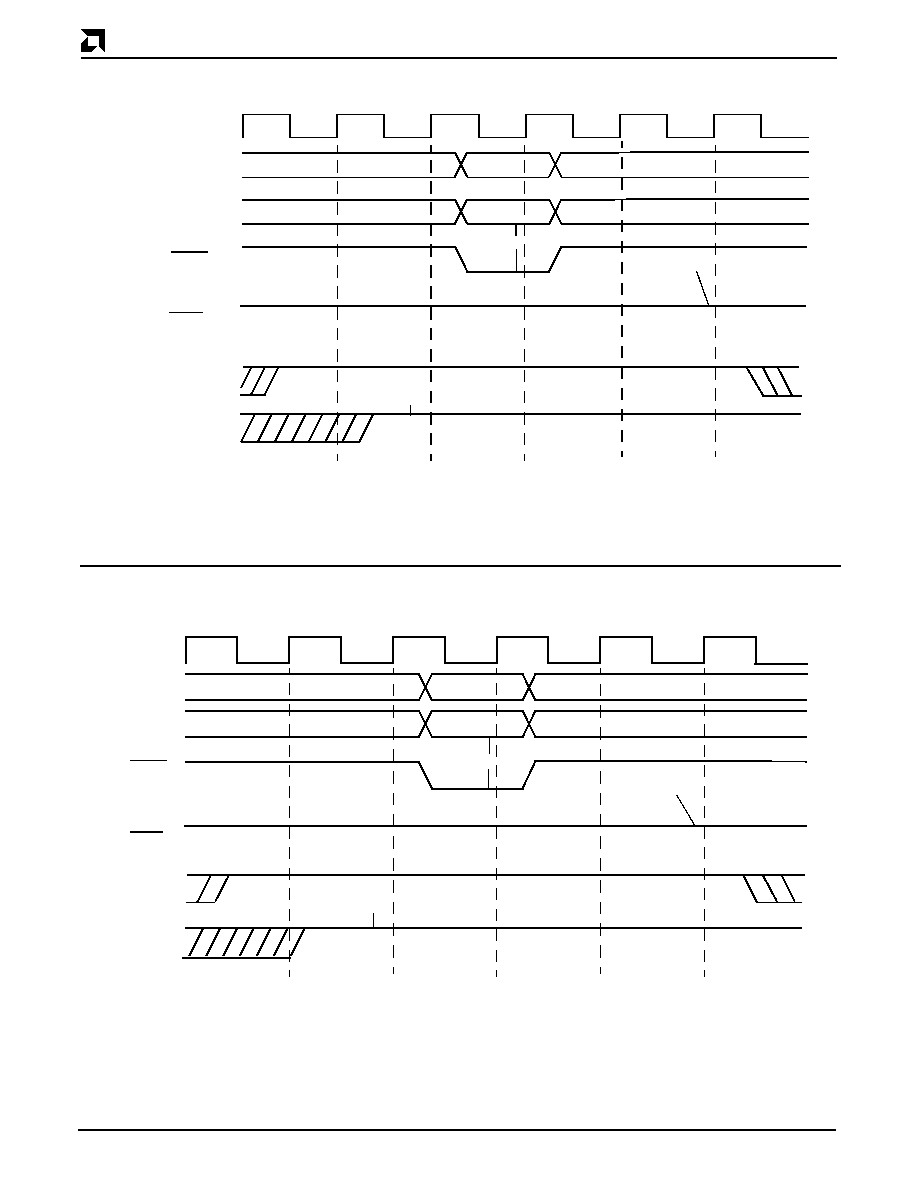
24
Am5
X
86 Microprocessor
AMD
PRELIMINARY
HLDA
EADS
HOLD
HITM
ADR
INV
CLK
valid
valid
Figure 6. Snoop of On-Chip Cache That Does Not Hit a Line
Note:
The circled numbers in this figure represent the steps in section 4.8.3.1.
HLDA
HOLD
HITM
EADS
INV
ADR
CLK
Note:
The circled numbers in this figure represent the steps in section 4.8.3.2.
Figure 7. Snoop of On-Chip Cache That Hits a Non-modified Line
valid
valid

Am5
X
86 Microprocessor
25
AMD
PRELIMINARY
4.8.3
External Bus Master Snooping Actions
The following scenarios describe the snooping actions
of an external bus master.
4.8.3.1
Snoop Miss
Scenario
: A snoop of the on-chip cache does not hit a
line, as shown in Figure 6.
Step 1 The microprocessor is placed in Snooping
mode with HOLD. HLDA must be High for a
minimum of one clock cycle before EADS as-
sertion. In the fastest case, this means that
HOLD was asserted one clock cycle before the
HLDA response.
Step 2 EADS and INV are applied to the microproces-
sor. If INV is 0, a read access caused the snoop-
ing cycle. If INV is 1, a write access caused the
snooping cycle.
Step 3 Two clock cycles after EADS is asserted, HITM
becomes valid. Because the addressed line is
not in the snooping cache, HITM is 1.
4.8.3.2
Snoop Hit to a Non-Modified Line
Scenario
: The snoop of the on-chip cache hits a line,
and the line is not modified (see Figure 7).
Step 1 The microprocessor is placed in Snooping
mode with HOLD. HLDA must be High for a
minimum of one clock cycle before EADS as-
sertion. In the fastest case, this means that
HOLD was asserted one clock cycle before the
HLDA response.
Step 2 EADS and INV are applied to the microproces-
sor. If INV is 0, a read access caused the snoop-
ing cycle. If INV is 1, a write access caused the
snooping cycle.
Step 3 Two clock cycles after EADS is asserted, HITM
becomes valid. In this case, HITM is 1.
4.8.4
Write-Back Case
Scenario
: Write-back accesses are always burst writes
with a length of four 32-bit words. For burst writes, the
burst always starts with the microprocessor line offset
at 0. HOLD must be deasserted before the write-back
can be performed (see Figure 8).
Step 1 HOLD places the microprocessor in Snooping
mode. HLDA must be High for a minimum of
one clock cycle before EADS assertion. In the
fastest case, this means that HOLD asserts one
clock cycle before the HLDA response.
Step 2 EADS and INV are asserted. If INV is 0, snoop-
ing is caused by a read access. If INV is 1,
snooping is caused by a write access. EADS is
not sampled again until after the modified line
is written back to memory. It is detected again
as early as in Step 11.
EADS
External
bus master's
BOFF signal
HLDA
Data
HOLD
HITM
ADS
INV
BRDY
BLAST
W/R
M/IO
ADR
CLK
valid
n
n
n
n+4
n+8 n+12
n+1
valid
n
Figure 8. Snoop That Hits a Modified Line (Write-Back)
Note:
The circled numbers in this figure represent the steps in section 4.8.4.
2
3
1
7
8
9
10
6
5
11
floating/tri-stated
CACHE
floating/tri-stated
4
n+8
n+4

26
Am5
X
86 Microprocessor
AMD
Step 3 Two clock cycles after EADS is asserted, HITM
becomes valid, and is 0 because the line is mod-
ified.
Step 4 In the next clock, the core system logic deas-
serts the HOLD signal in response to the
HITM = 0 signal. The core system logic backs
off the current bus master at the same time so
that the microprocessor can access the bus.
HOLD can be reasserted immediately after
ADS is asserted for burst cycles.
Step 5 The snooping cache starts it's write-back of the
modified line by asserting ADS = 0, CACHE = 0,
and W/R = 1. The write access is a burst write.
The number of clock cycles between deassert-
ing HOLD to the snooping cache and first
asserting ADS for the write-back cycles can
vary. In this example, it is one clock cycle, which
is the shortest possible time. Regardless of the
number of clock cycles, the start of the write-
back is seen by ADS going Low.
Step 6 The write-back access is finished when BLAST
and BRDY both are 0.
Step 7 In the clock cycle after the final write-back ac-
cess, the processor drives HITM back to 1.
Step 8 HOLD is sampled by the microprocessor.
Step 9 One cycle after sampling HOLD High, the mi-
croprocessor transitions HLDA transitions to 1,
acknowledging the HOLD request.
Step 10 The core system logic removes hold-off control
to the external bus master. This allows the ex-
ternal bus master to immediately retry the abort-
ed access. ADS is strobed Low, which
generates EADS Low in the same clock cycle.
Step 11 The bus master restarts the aborted access.
EADS and INV are applied to the microproces-
sor as before. This starts another snoop cycle.
The status of the addressed line is now either shared
(INV = 0) or is changed to invalid (INV = 1).
4.8.5
Write-Back and Pending Access
Scenario
: The following occurs when, in addition to the
write-back operation, other bus accesses initiated by
the processor associated with the snooped cache are
pending. The microprocessor gives the write-back ac-
cess priority. This implies that if HOLD is deasserted,
the microprocessor first writes back the modified line
(see Figure 9).
Figure 9. Write-Back and Pending Access
Note:
The circled numbers in this figure represent the steps in section 4.8.5.
EADS
External
bus master's
BOFF signal
HLDA
Data
HOLD
HITM
ADS
INV
BRDY
BLAST
W/R
M/IO
ADR
CLK
valid
n
n
n
n+4
n+8 n+12
n+12
valid
n
2
3
1
7
8
9
10
6
5
11
floating/tri-stated
CACHE
4
n+8
n+4
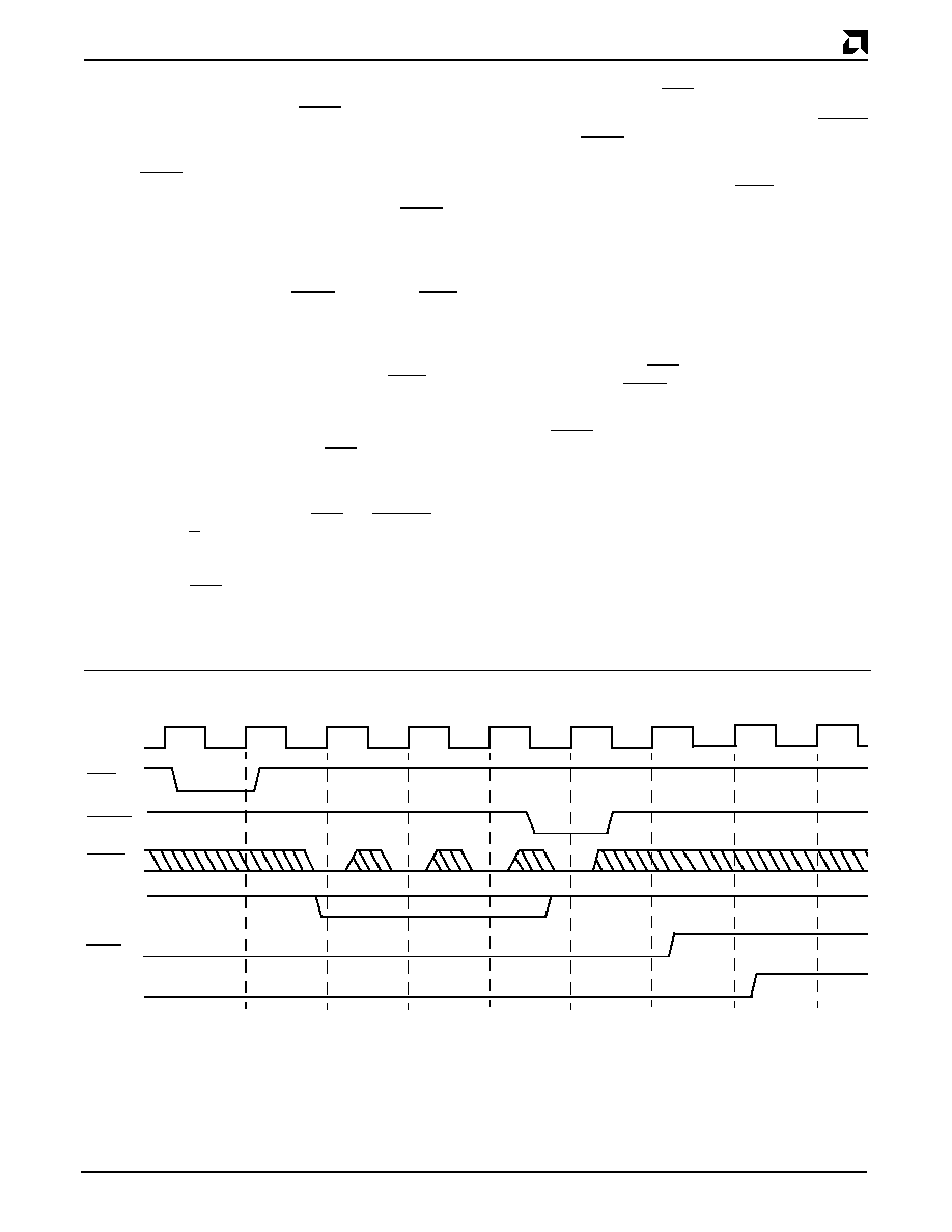
Am5
X
86 Microprocessor
27
AMD
PRELIMINARY
Step 1 HOLD places the microprocessor in Snooping
mode. HLDA must be High for a minimum of
one clock cycle before EADS assertion. In the
fastest case, this means that HOLD asserts one
clock cycle before the HLDA response.
Step 2 EADS and INV are asserted. If INV is 0, snoop-
ing is caused by a read access. If INV is 1,
snooping is caused by a write access. EADS is
not sampled again until after the modified line
is written back to memory. It is detected again
as early as in Step 11.
Step 3 Two clock cycles after EADS is asserted, HITM
becomes valid, and is 0 because the line is
modified.
Step 4 In the next clock the core system logic deasserts
the HOLD signal in response to the HITM = 0.
The core system logic backs off the current bus
master at the same time so that the micropro-
cessor can access the bus. HOLD can be re-
asserted immediately after ADS is asserted for
burst cycles.
Step 5 The snooping cache starts its write-back of the
modified line by asserting ADS = 0, CACHE = 0,
and W/R = 1. The write access is a burst write.
The number of clock cycles between deassert-
ing HOLD to the snooping cache and first as-
serting ADS for the write-back cycles can vary.
In this example, it is one clock cycle, which is
the shortest possible time. Regardless of the
number of clock cycles, the start of the write-
back is seen by ADS going Low.
Step 6 The write-back access is finished when BLAST
and BRDY both are 0.
Step 7 In the clock cycle after the final write-back ac-
cess, the processor drives HITM back to 1.
Step 8 HOLD is sampled by the microprocessor.
Step 9 A minimum of 1 clock cycle after the completion
of the pending access, HLDA transitions to 1,
acknowledging the HOLD request.
Step 10 The core system logic removes hold-off control
to the external bus master. This allows the ex-
ternal bus master to immediately retry the abort-
ed access. ADS is strobed Low, which
generates EADS Low in the same clock cycle.
Step 11 The bus master restarts the aborted access.
EADS and INV are applied to the microproces-
sor as before. This starts another snoop cycle.
The status of the addressed line is now either shared
(INV = 0) or is changed to invalid (INV = 1).
4.8.5.1
HOLD/HLDA Write-Back Design
Considerations
When designing a write-back cache system that uses
HOLD/HLDA as the bus arbitration method, the follow-
ing considerations must be observed to ensure proper
operation (see Figure 10).
HLDA
CLK
ADS
BLAST
BRDY
HOLD
Valid Hold Assertion
Figure 10. Valid HOLD Assertion During Write-Back
HITM

28
Am5
X
86 Microprocessor
AMD
PRELIMINARY
Step 1 During a snoop to the on-chip cache that hits a
modified cache line, the HOLD signal cannot
be deasserted to the microprocessor until the
next clock cycle after HITM transitions active.
Step 2 After the write-back has commenced, the HOLD
signal should be asserted no earlier than the
next clock cycle after ADS goes active, and no
later than in the final BRDY of the last write.
Asserting HOLD later than the final BRDY may
allow the microprocessor to permit a pending
access to begin.
Step 3 If RDY is returned instead of BRDY during a
write-back, the HOLD signal can be reasserted
at any time starting one clock after ADS goes
active in the first transfer up to the final transfer
when RDY is asserted. Asserting RDY instead
of BRDY will not break the write-back cycle if
HOLD is asserted. The processor ignores
HOLD until the final write cycle of the write-back.
4.8.5.2
AHOLD Bus Arbitration Implementation
The use of AHOLD as the control mechanism is often
found in systems where an external second-level cache
is closely coupled to the microprocessor. This tight cou-
pling allows the microprocessor to operate with the least
amount of stalling from external snooping of the on-chip
cache. Additionally, snooping of the cache can be per-
formed concurrently with an access by the microproces-
sor. This feature further improves the performance of
the total system (see Figure 11).
Note: To maintain proper system timing, the AHOLD
signal must remain active for one clock cycle after HITM
transitions active. Deassertion of AHOLD in the same
clock cycle as HITM assertion may lead to unpredictable
processor behavior.
DRAM
Address Bus
Data Bus
L2 Cache
Address Bus
Data Bus
I/O Bus
Interface
Slow
Peripheral
CPU
Address Bus
Data Bus
Figure 11. Closely Coupled Cache Block Diagram
The following sections describe the snooping scenarios
for the AHOLD implementation.
4.8.5.3
Normal Write-Back
Scenario
: This scenario assumes that a processor-ini-
tiated access has already started and that the external
logic can finish that access even without the address
being applied after the first clock cycle. Therefore, a
snooping access with AHOLD can be done in parallel.
In this case, the processor-initiated access is finished
first, then the write-back is executed (see Figure 12).
The sequence is as follows:
Step 1 The processor initiates an external, simple,
non-cacheable read access, strobing ADS = 0
and W/R = 0. The address is driven from the
CPU.
Step 2 In the same cycle, AHOLD is asserted to indi-
cate the start of snooping. The address bus
floats and becomes an input in the next clock
cycle.
Step 3 During the next clock cycles, the BRDY or RDY
signal is not strobed Low. Therefore, the pro-
cessor-initiated access is not finished.
Step 4 Two clock cycles after AHOLD is asserted, the
EADS signal is activated to start an actual
snooping cycle, and INV is valid. If INV is 0, a
read access caused the snooping cycle. If INV
is 1, a write access caused the snooping cycle.
Additional EADS are ignored due to the hit of a
modified line. It is detected after HITM goes in-
active.
Step 5 Two clock cycles after EADS is asserted, the
snooping signal HITM becomes valid. The line
is modified; therefore, HITM is 0.
Step 6 In this cycle, the processor-initiated access is
finished.
Step 7 Two clock cycles after the end of the processor-
initiated access, the cache immediately starts
writing back the modified line. This is indicated
by ADS = 0 and W/R = 1. Note that AHOLD is
still active and the address bus is still an input.
However, the write-back access can be execut-
ed without any address. This is because the
corresponding address must have been on the
bus when EADS was strobed. Therefore, in the
case of the core system logic, the address for
the write-back must be latched with EADS to
be available later. This is required only if
AHOLD is not removed if HITM becomes 0.
Otherwise, the address of the write-back is put
onto the address bus by the microprocessor.

Am5
X
86 Microprocessor
29
AMD
PRELIMINARY
10
9
Data
HITM
EADS
INV
Read
BRDY
AHOLD
BLAST
ADS
W/R
M/IO
ADR
CLK
W n+4
W n
W n+8
W n+C
Figure 12. Snoop Hit Cycle with Write-Back
Note:
The circled numbers in this figure represent the steps in section 4.8.5.3.
1
7
8
5
4
6
3
2
CACHE
from CPU
to CPU
from CPU
Step 8 As an example, AHOLD is now removed. In the
next clock cycle, the current address of the
write-back access is driven onto the address
bus.
Step 9 The write-back access is finished when BLAST
and BRDY both transition to 0.
Step 10 In the clock cycle after the final write-back
access, the snooping cache drives HITM back
to 1.
The status of the snooped and written-back line is now
either shared (INV = 0) or is changed to invalid (INV = 1).
4.8.6
Reordering of Write-Backs (AHOLD) with
BOFF
As seen previously, the Bus Interface Unit (BIU) com-
pletes the processor-initiated access first if the snooping
access occurs after the start of the processor-initiated
access. If the HITM signal occurs one clock cycle before
the ADS = 0 of the processor-initiated access, the write-
back receives priority and is executed first.
However, if the snooping access is executed after the
start of the processor-initiated access, there is a
methodology to reorder the access order. The BOFF
signal delays outstanding processor-initiated cycles so
that a snoop write-back can occur immediately (see
Figure 13).
Scenario
: If there are outstanding processor-initiated
cycles on the bus, asserting BOFF clears the bus pipe-
line. If a snoop causes HITM to be asserted, the first
cycle issued by the microprocessor after deassertion of
BOFF is the write-back cycle. After the write-back cycle,
it reissues the aborted cycles. This translates into the
following sequence:
Step 1 The processor starts a cacheable burst read
cycle.
Step 2 One clock cycle later, AHOLD is asserted. This
switches the address bus into an input one clock
cycle after AHOLD is asserted.
Step 3 Two clock cycles after AHOLD is asserted, the
EADS and INV signals are asserted to start the
snooping cycle.
Step 4 Two clock cycles after EADS is asserted, HITM
becomes valid. The line is modified, therefore
HITM = 0.
Step 5 Note that the processor-initiated access is not
completed because BLAST = 1.
Step 6 With HITM going Low, the core system logic
asserts BOFF in the next clock cycle to the
snooping processor to reorder the access.
BOFF overrides BRDY. Therefore, the partial
read is not used. It is reread later.

30
Am5
X
86 Microprocessor
AMD
PRELIMINARY
Step 7 One clock cycle later BOFF is deasserted. The
write-back access starts one clock cycle later
because the BOFF has cleared the bus pipe-
line.
Step 8 AHOLD is deasserted. In the next clock cycle
the address for the write-back is driven on the
address bus.
Step 9 One cycle after BOFF is deasserted, the cache
immediately starts writing back the modified
line. This is indicated by ADS = 0 and W/R = 1.
Step 10 The write-back access is finished when BLAST
and BRDY go active 0.
Step 11 The BIU restarts the aborted cache line fill with
the previous read. This is indicated by ADS = 0
and W/R = 0.
Step 12 In the same clock cycle, the snooping cache
drives HITM back to 1.
Step 13 The previous read is now reread.
4.8.7
Special Scenarios for AHOLD Snooping
In addition to the previously described scenarios, there
are special scenarios regarding the time of the EADS
and AHOLD assertion. The final result depends on the
time EADS and AHOLD are asserted relative to other
processor-initiated operations.
4.8.7.1
Write Cycle Reordering due to Buffering
Scenario
: The MESI cache protocol and the ability to
perform and respond to snoop cycles guarantee that
writes to the cache are logically equivalent to writes to
memory. In particular, the order of read and write oper-
ations on cached data is the same as if the operations
were on data in memory. Even non-cached memory
read and write requests usually occur on the external
bus in the same order that they were issued in the pro-
gram. For example, when a write miss is followed by a
read miss, the write data goes on the bus before the
read request is put on the bus. However, the posting of
writes in write buffers coupled with snooping cycles may
cause the order of writes seen on the external bus to
differ from the order they appear in the program. Con-
sider the following example, which is illustrated in Figure
14. For simplicity, snooping signals that behave in their
usual manner are not shown.
Step 1 AHOLD is asserted. No further processor-initi-
ated accesses to the external bus can be start-
ed. No other access is in progress.
Step 2 The processor writes data A to the cache, re-
sulting in a write miss. Therefore, the data is put
into the write buffers, assuming they are not full.
No external access can be started because
AHOLD is still 1.
R2
BOFF
Data
HITM
EADS
INV
AHOLD
R1
BRDY
BLAST
ADS
W/R
M/IO
ADR
CLK
W1 to CPU
don't care
W1
W2
W3
W4
W1 from CPU
W3
W4
Figure 13. Cycle Reordering with BOFF (Write-Back)
Note:
The circled numbers in this figure represent the steps in section 4.8.6.
W2
11
12
R2 from CPU
CACHE
R1 from CPU

Am5
X
86 Microprocessor
31
AMD
PRELIMINARY
Step 10 In the same clock cycle, the snooping cache
drives HITM back to 1.
Step 11 The write of data A is finished if BRDY transi-
tions to 0 (BLAST = 0), because it is a single
word.
The software write sequence was first data A and then
data B. But on the external bus the data appear first as
data B and then data A. The order of writes is changed.
In most cases, it is unnecessary to strictly maintain the
ordering of writes. However, some cases (for example,
writing to hardware control registers) require writes to
be observed externally in the same order as pro-
grammed. There are two options to ensure serialization
of writes, both of which drive the cache to Write-through
mode:
1.
Set the PWT bit in the page table entries.
2.
Drive the WB/WT signal Low when accessing these
memory locations.
Option 1 is an operating-system-level solution not di-
rectly implemented by user-level code. Option 2, the
hardware solution, is implemented at the system level.
BLAST
Data
BRDY
EADS
ADS
HITM
Cached Data
AHOLD
CLK
Write Buffer
B original
1
A
2
6
5
B modified
4
3
B
B+4
B+8
B+12
8
A
Ignored
9
7
XXX
Note:
The circled numbers in this figure represent the steps in section 4.8.7.1.
Figure 14. Write Cycle Reordering Due to Buffering
10
11
Step 3 The next write of the processor hits the cache
and the line is non-shared. Therefore, data B is
written into the cache. The cache line transits
to the modified state.
Step 4 In the same clock cycle, a snoop request to the
same address where data B resides is started
because EADS = 0. The snoop hits a modified
line. EADS is ignored due to the hit of a modified
line, but is detected again as early as in step 10.
Step 5 Two clock cycles after EADS asserts, HITM be-
comes valid.
Step 6 Because the processor-initiated access cannot
be finished (AHOLD is still 1), the BIU gives
priority to a write-back access that does not re-
quire the use of the address bus. Therefore, in
the clock cycle, the cache starts the write-back
sequence indicated by ADS = 0 and W/R = 0.
Step 7 During the write-back sequence, AHOLD is
deasserted.
Step 8 The write-back access is finished when BLAST
and BRDY transition to 0.
Step 9 After the last write-back access, the BIU starts
writing data A from the write buffers. This is
indicated by ADS = 0 and W/R = 0.

32
Am5
X
86 Microprocessor
AMD
PRELIMINARY
4.8.7.2
BOFF Write-Back Arbitration
Implementation
The use of BOFF to perform snooping of the on-chip
cache is used in systems where more than one cache-
able bus master resides on the microprocessor bus. The
BOFF signal forces the microprocessor to relinquish the
bus in the following clock cycle, regardless of the type
of bus cycle it was performing at the time. Consequently,
the use of BOFF as a bus arbitrator should be imple-
mented with care to avoid system problems.
4.8.8
BOFF Design Considerations
The use of BOFF as a bus arbitration control mechanism
is immediate. BOFF forces the microprocessor to abort
an access in the following clock cycle after it is asserted.
The following design issues must be considered.
4.8.8.1
Cache Line Fills
The microprocessor aborts a cache line fill during a burst
read if BOFF is asserted during the access. Upon re-
gaining the bus, the read access commences where it
left off when BOFF was recognized. External buffers
should take this cycle continuation into consideration if
BOFF is allowed to abort burst read cycles.
4.8.8.2
Cache Line Copy-Backs
Similar to the burst read, the burst write also can be
aborted at any time with the BOFF signal. Upon regain-
ing access to the bus, the write continues from where it
was aborted. External buffers and control logic should
take into consideration the necessary control, if any, for
burst write continuations.
4.8.8.3
Locked Accesses
Locked bus cycles occur in various forms. Locked ac-
cesses occur during read-modify-write operations, in-
terrupt acknowledges, and page table updates.
Although asserting BOFF during a locked cycle is per-
mitted, extreme care should be taken to ensure data
coherency for semaphore updates and proper data or-
dering.
4.8.9
BOFF During Write-Back
If BOFF is asserted during a write-back, the processor
performing the write-back goes off the bus in the next
clock cycle. If BOFF is released, the processor restarts
that write-back access from the point at which it was
aborted. The behavior is identical to the normal BOFF
case that includes the abort and restart behavior.
4.8.10 Snooping Characteristics During a Cache
Line Fill
The microprocessor takes responsibility for responding
to snoop cycles for a cache line only during the time that
the line is actually in the cache or in a copy-back buffer.
There are times during the cache line fill cycle and during
the cache replacement cycle when the line is "in transit"
and snooping responsibility must be taken by other sys-
tem components.
The following cases apply if snooping is invoked via
AHOLD, and neither HOLD nor BOFF is asserted.
s
System designers should consider the possibility
that a snooping cycle may arrive at the same time
as a cache line fill or replacement for the same ad-
dress. If a snooping cycle arrives at the same time
as a cache line fill with the same address, the CPU
uses the cache line fill, but does not place it in the
cache.
s
If a snooping cycle occurs at the same time as a
cache line fill with a different address, the cache line
fill is placed into the cache unless EADS is recog-
nized before the first BRDY but after ADS is assert-
ed, or EADS is recognized on the last BRDY of the
cache line fill. In these cases, the line is not placed
into the cache.
4.8.11 Snooping Characteristics During a
Copy-Back
If a copy-back is occurring because of a cache line re-
placement, the address being replaced can be matched
by a snoop until assertion of the last BRDY of the copy-
back. This is when the modified line resides in the copy-
back buffer. An EADS as late as two clocks before the
last BRDY can cause HITM to be asserted.
Figure 15 illustrates the microprocessor relinquishing
responsibility of recognizing snoops for a line that is
copied back. It shows the latest EADS assertion that
can cause HITM assertion. HITM remains active for only
one clock period in that example. HITM remains active
through the last BRDY of the corresponding write-back;
in that case, the write-back has already completed. This
is the latest point where snooping can start, because
two clock cycles later, the final BRDY of the write-back
is applied.
If a snoop cycle hits the copy-back address after the first
BRDY of the copy-back and ADS has been issued, the
microprocessor asserts HITM. Keep in mind that the
write-back was initiated due to a read miss and not due
to a snoop to a modified line. In the second case, no
snooping is recognized if a modified line is detected.

Am5
X
86 Microprocessor
33
AMD
PRELIMINARY
4.9
Cache Invalidation and Flushing in
Write-Back Mode
The Am5
X
86 microprocessor family supports cache in-
validation and flushing, much like the Am486 micropro-
cessor Write-through mode. However, the addition of
the write-back cache adds some complexity.
4.9.1
Cache Invalidation through Software
To invalidate the on-chip cache, the Am5
X
86 micropro-
cessor family uses the same instructions as the Am486
microprocessor family. The two invalidation instruc-
tions, INVD and WBINVD, while similar, are slightly dif-
ferent for use in the write-back environment.
The WBINVD instruction first performs a write-back of
the modified data in the cache to external memory. Then
it invalidates the cache, followed by two special bus
cycles. The INVD instruction only invalidates the cache,
regardless of whether modified data exists, and follows
with a special bus cycle. The utmost care should be
taken when executing the INVD instruction to ensure
memory coherency. Otherwise, modified data may be
invalidated prior to writing back to main memory. In
Write-back mode, WBINVD requires a minimum of 4100
internal clocks to search the cache for modified data.
Writing back modified data adds to this minimum time.
WBINVD can only be stopped by a RESET.
Two special bus cycles follow the write-back of modified
data upon execution of the WBINVD instruction: first the
write-back, and then the flush special bus cycle. The
INVD operates identically to the standard 486 micropro-
cessor family in that the flush special bus cycle is gen-
erated when the on-chip cache is invalidated. Table 7
specifies the special bus cycle states for the instructions
WBINVD and INVD.
4.9.2
Cache Invalidation through Hardware
The other mechanism for cache invalidation is the
FLUSH pin. The FLUSH pin operates similarly to the
WBINVD command, writing back modified cache lines
to main memory. After the entire cache has copied back
all the modified data, the microprocessor generates two
special bus cycles. These special bus cycles signal to
the external caches that the microprocessor on-chip
cache has completed its copy-back and that the second
level cache may begin its copy-back to memory, if so
required.
Two flush acknowledge cycles are generated after the
FLUSH pin is asserted and the modified data in the
cache is written back. As with the WBINVD instruction,
in Write-back mode, a flush requires a minimum of 4100
internal clocks to test the cache for modified data. Writ-
ing back modified data adds to this minimum time. The
flush operation can only be stopped by a RESET. Table
8 shows the special flush bus cycle configuration.
Table 7. WBINVD/INVD Special Bus Cycles
A32≠A2
M/IO D/C W/R BE3 BE2 BE1 BE0 Bus Cycle
0000 0000 h
0
0
1
0
1
1
1
Write-back
1
0000 0000 h
0
0
1
1
1
0
1
Flush
1, 2
Notes:
1. WBINVD generates first write-back, then flush.
2. INVD generates only flush.
BRDY
BLAST
ADS
HITM
EADS
AHOLD
ADR
CLK
n
S
Figure 15. Latest Snooping of Copy-Back
CACHE
Address B

34
Am5
X
86 Microprocessor
AMD
PRELIMINARY
4.9.3
Snooping During Cache Flushing
As with snooping during normal operation, snooping is
permitted during a cache flush, whether initiated by the
FLUSH pin or WBINVD instruction. After completion of
the snoop, and write-back, if needed, the microproces-
sor completes the copy-back of modified cache lines.
4.10 Burst Write
The Am5
X
86 microprocessor improves system perfor-
mance by implementing a burst write feature for cache
line write-backs and copy-backs. Standard write oper-
ations are still supported. Burst writes are always four
32-bit words and start at the beginning of a cache line
address of 0 for the starting access. The timing of the
BLAST and BRDY signals is identical to the burst read.
Figure 16 shows a burst write access. (See Figure 17
and Figure 18 for burst read and burst write access with
BOFF asserted.) In addition to using BLAST, the
CACHE signal indicates burstable cycles.
CACHE is a cycle definition pin used when in Write-back
mode (CACHE floats in Write-through mode). For pro-
cessor-initiated cycles, the signal indicates:
s
For a read cycle, the internal cacheability of the cycle
s
For a write cycle, a burst write-back or copy-back, if
KEN is asserted (for linefills).
Table 8. FLUSH Special Bus Cycles
A32≠A2
M/IO D/C W/R BE3 BE2 BE1 BE0 Bus Cycle
0000 0001h
0
0
1
0
1
1
1
First Flush
Acknowledge
0000 0001h
0
0
1
1
1
0
1
Second
Flush
Acknowledge
W/R
BRDY
ADS
BLAST
ADR
M/IO
XX4
Data
XX0
XX0
XX4
XX8
XXC
Figure 16. Burst Write
CLK
CACHE
XXC
XX8
Data
to CPU
BRDY
BOFF
XX0
XX4
don't care
ADR
XX0
ADS
BLAST
M/IO
W/R
CLK
XX4
XX4
XX8
XXC
XX4
XX8
XXC
Figure 17. Burst Read with BOFF Assertion
CACHE

Am5
X
86 Microprocessor
35
AMD
PRELIMINARY
Data
from CPU
BRDY
BOFF
XX4
ADR
ADS
BLAST
M/IO
W/R
CLK
Figure 18. Burst Write with BOFF Assertion
CACHE
XX0
XX4
XX4
XX8
XXC
XX0
XX8
XXC
XX4
CACHE is asserted for cacheable reads, cacheable
code fetches, and write-backs/copy-backs. CACHE is
deasserted for non-cacheable reads, translation looka-
side buffer (TLB) replacements, locked cycles (except
for write-back cycles generated by an external snoop
operation that interrupts a locked read/modify/write se-
quence), I/O cycles, special cycles, and write-throughs.
CACHE is driven to its valid level in the same clock as
the assertion of ADS and remains valid until the next
RDY or BRDY assertion. The CACHE output pin floats
one clock after BOFF is asserted. Additionally, the signal
floats when HLDA is asserted.
The following steps describe the burst write sequence:
1.
The access is started by asserting: ADS = 0, M/IO
= 1, W/R = 1, CACHE = 0. The address offset always
is 0, so the burst write always starts on a cache line
boundary. CACHE transitions High (inactive) after
the first BRDY.
2.
In the second clock cycle, BLAST is 1 to indicate
that the burst is not finished.
3.
The burst write access is finished when BLAST is
0 and BRDY is 0.
When the RDY signal is returned instead of the BRDY
signal, the Am5
X
86 microprocessor halts the burst cycle
and proceeds with the standard non-burst cycle.
4.10.1 Locked Accesses
Locked accesses of an Am5
X
86 microprocessor occur
for read-modify-write operations and interrupt acknowl-
edge cycles. The timing is identical to the DX micropro-
cessor, although the state transitions differ from the
standard DX microprocessor. Unlike processor-initiated
accesses, state transitions for locked accesses are seen
by all processors in the system. Any locked read or write
generates an external bus cycle, regardless of cache
hit or miss. During locked cycles, the processor does
not recognize a HOLD request, but it does recognize
BOFF and AHOLD requests.
Locked read operations always read data from the ex-
ternal memory, regardless of whether the data is in the
cache. In the event that the data is in the cache and
unmodified, the cache line is invalidated and an external
read operation is performed. The data from the external
memory is used instead of the data in the cache, thus
ensuring that the locked read is seen by all other bus
masters. If a locked read occurs, the data is in the cache,
and it is modified. The microprocessor first copies back
the data to external memory, invalidates the cache line,
and then performs a read operation to the same location,
thus ensuring that the locked read is seen by all other
bus masters. At no time is the data in the cache used
directly by the microprocessor or a locked read opera-
tion before reading the data from external memory.
Since locked cycles always begin with a locked read
access, and locked read cycles always invalidate a
cache line, a locked write cycle to a valid cache line,
either modified or unmodified, does not occur.
4.10.2 Serialization
Locked accesses are totally serialized:
s
All reads and writes in the write buffer that precede
the locked access are issued on the bus before the
first locked access is executed.
s
No read or write after the last locked access is issued
internally or on the bus until the final RDY or BRDY
for all locked accesses.
s
It is possible to get a locked read, write-back, locked
write cycle.

36
Am5
X
86 Microprocessor
AMD
PRELIMINARY
4.10.3 PLOCK Operation in Write-Through Mode
As described in Section 3, PLOCK is only used in Write-
through mode; the signal is driven inactive in Write-back
mode. In Write-through mode, the processor drives
PLOCK Low to indicate that the current bus transaction
requires more than one bus cycle. The CPU continues
to drive the signal Low until the transaction is completed,
whether or not RDY or BRDY is returned. Refer to the
pin description for additional information.
5
CLOCK CONTROL
5.1
Clock Generation
The Am5
X
86 CPU is driven by a 1x clock that relies on
phased-lock loop (PLL) to generate the two internal
clock phases: phase one and phase two. The rising edge
of CLK corresponds to the start of phase one (ph1). All
external timing parameters are specified relative to the
rising edge of CLK.
5.2
Stop Clock
The Am5
X
86 CPU also provides an interrupt mecha-
nism, STPCLK, that allows system hardware to control
the power consumption of the CPU by stopping the in-
ternal clock to the CPU core in a sequenced manner.
The first low-power state is called the Stop Grant state.
If the CLK input is completely stopped, the CPU enters
into the Stop Clock state (the lowest power state). When
the CPU recognizes a STPCLK interrupt, the processor:
s
Stops execution on the next instruction boundary
(unless superseded by a higher priority interrupt)
s
Waits for completion of cache flush
s
Stops the pre-fetch unit
s
Empties all internal pipelines and write buffers
s
Generates a Stop Grant bus cycle
s
Stops the internal clock
At this point the CPU is in the Stop Grant state.
The CPU cannot respond to a STPCLK request from an
HLDA state because it cannot empty the write buffers
and, therefore, cannot generate a Stop Grant cycle. The
rising edge of STPCLK signals the CPU to return to
program execution at the instruction following the inter-
rupted instruction. Unlike the normal interrupts (INTR
and NMI), STPCLK does not initiate interrupt acknowl-
edge cycles or interrupt table reads.
5.2.1
External Interrupts in Order of Priority
In Write-through mode, the priority order of external in-
terrupts is:
1. RESET/SRESET
2. FLUSH
3. SMI
4. NMI
5. INTR
6. STPCLK
In Write-back mode, the priority order of external inter-
rupts is:
1. RESET
2. FLUSH
3. SRESET
4. SMI
5. NMI
6. INTR
7. STPCLK
STPCLK is active Low and has an internal pull-up re-
sistor. STPCLK is asynchronous, but setup and hold
times must be met to ensure recognition in any specific
clock. STPCLK must remain active until the Stop Grant
special bus cycle is asserted and the system responds
with either RDY or BRDY. When the CPU enters the
Stop Grant state, the internal pull-up resistor is disabled,
reducing the CPU power consumption. The STPCLK
input must be driven High (not floated) to exit the Stop
Grant state. STPCLK must be deasserted for a minimum
of five clocks after RDY or BRDY is returned active for
the Stop Grant bus cycle before being asserted again.
There are two regions for the Low-power mode supply
current:
1.
Low Power:
Stop Grant state (fast wake-up, frequency-
and voltage-dependent)
2.
Lowest Power:
Stop Clock state (slow wake-up, volt-
age-dependent)
5.3
Stop Grant Bus Cycle
The processor drives a special Stop Grant bus cycle to
the bus after recognizing the STPCLK interrupt. This
bus cycle is the same as the HALT cycle used by a
standard Am486 microprocessor, with the exception
that the Stop Grant bus cycle drives the value 0000
0010h on the address pins.
s
M/lO = 0
s
D/C = 0
s
W/R =1
s
Address Bus = 0000 0010h (A
4
= 1)
s
BE3≠BE0 = 1011
s
Data bus = undefined
The system hardware must acknowledge this cycle by
returning RDY or BRDY, or the processor will not enter
the Stop Grant state (see Figure 19). The latency be-
tween a STPCLK request and the Stop Grant bus cycle
depends on the current instruction, the amount of data
in the CPU write buffers, and the system memory per-
formance.

Am5
X
86 Microprocessor
37
AMD
PRELIMINARY
5.4
Pin State During Stop Grant
Table 9 shows the pin states during Stop Grant Bus
states. During the Stop Grant state, most output and
input/output signals of the microprocessor maintain the
level they held when entering the Stop Grant state. The
data and data parity signals are tri-stated. In response
to HOLD being driven active during the Stop Grant state
(when the CLK input is running), the CPU generates
HLDA and tri-states all output and input/output signals
that are tri-stated during the HOLD/HLDA state. After
HOLD is deasserted, all signals return to the same state
they were before the HOLD/HLDA sequence.
To achieve the lowest possible power consumption dur-
ing the Stop Grant state, the system designer must en-
sure that the input signals with pull-up resistors are not
driven Low, and the input signals with pull-down resis-
tors are not driven High.
All inputs except data bus pins must be driven to the
power supply rails to ensure the lowest possible current
consumption during Stop Grant or Stop Clock modes.
For compatibility, data pins must be driven Low to
achieve the lowest possible power consumption.
5.5
Clock Control State Diagram
Figure 20 shows the state transitions during a Stop
Clock cycle.
5.5.1
Normal State
This is the normal operating state of the CPU. While in
the normal state, the CLK input can be dynamically
changed within the specified CLK period stability limits.
5.5.2
Stop Grant State
The Stop Grant state provides a low-power state that
can be entered by simply asserting the external STPCLK
interrupt pin. When the Stop Grant bus cycle has been
placed on the bus, and either RDY or BRDY is returned,
the CPU is in this state. The CPU returns to the normal
execution state 10≠20 clock cycles after STPCLK has
been deasserted.
While in the Stop Grant state, the pull-up resistors on
STPCLK and UP are disabled internally. The system
must continue to drive these inputs to the state they
were in immediately before the CPU entered the Stop
Grant State. For minimum CPU power consumption, all
other input pins should be driven to their inactive level
while the CPU is in the Stop Grant state.
Table 9. Pin State During Stop Grant Bus State
Signal
Type
State
A3≠A2
O
Previous State
A31≠A4
I/O
Previous State
D31≠D0
I/O
Floated
BE3≠BE0
O
Previous State
DP3≠DP0
I/O
Floated
W/R, D/C, M/IO, CACHE
O
Previous State
ADS
O
Inactive
LOCK, PLOCK
O
Inactive
BREQ
O
Previous State
HLDA
O
As per HOLD
BLAST
O
Previous State
FERR
O
Previous State
PCHK
O
Previous State
SMIACT
O
Previous State
HITM
O
Previous State
.
t
20
t
21
Figure 19. Entering Stop Grant State
RDY
ADDR
STPCLK
CLK
Stop Grant Bus cycle

38
Am5
X
86 Microprocessor
AMD
PRELIMINARY
Figure 20. Stop Clock State Machine
(valid for Write-back mode only)
Figure 21. Recognition of Inputs when Exiting Stop Grant State
t
20
t
21
CLK
STPCLK
NMI
SMI
A
STPCLK
Sampled
Note: A = Earliest time at which NMI or SMI is recognized.
A RESET or SRESET brings the CPU from the Stop
Grant state to the Normal state. The CPU recognizes
the inputs required for cache invalidations (HOLD,
AHOLD, BOFF, and EADS) as explained later. The CPU
does not recognize any other inputs while in the Stop
Grant state. Input signals to the CPU are not recognized
until 1 clock after STPCLK is deasserted (see Figure 21).
While in the Stop Grant state, the CPU does not recog-
nize transitions on the interrupt signals (SMI, NMI, and
INTR). Driving an active edge on either SMI or NMI does
not guarantee recognition and service of the interrupt
request following exit from the Stop Grant state. How-
ever, if one of the interrupt signals (SMI, NMI, or INTR)
is driven active while the CPU is in the Stop Grant state,
and held active for at least one CLK after STPCLK is
deasserted, the corresponding interrupt will be serviced.

Am5
X
86 Microprocessor
39
AMD
PRELIMINARY
The Am5
X
86 CPU product family requires INTR to be
held active until the CPU issues an interrupt acknowl-
edge cycle to guarantee recognition. This condition also
applies to the existing Am486 CPUs.
In the Stop Grant state, the system can stop or change
the CLK input. When the clock stops, the CPU enters
the Stop Clock state. The CPU returns to the Stop Grant
state immediately when the CLK input is restarted. You
must hold the STPCLK input Low until a stabilized fre-
quency has been maintained for at least 1 ms to ensure
that the PLL has had sufficient time to stabilize.
The CPU generates a Stop Grant bus cycle when en-
tering the state from the Normal or the Auto HALT Power
Down state. When the CPU enters the Stop Grant state
from the Stop Clock state or the Stop Clock Snoop state,
the CPU does not generate a Stop Grant bus cycle.
5.5.3
Stop Clock State
Stop Clock state is entered from the Stop Grant state
by stopping the CLK input (either logic High or logic
Low). None of the CPU input signals should change
state while the CLK input is stopped. Any transition on
an input signal (except INTR) before the CPU has re-
turned to the Stop Grant state may result in unpredict-
able behavior. If INTR goes active while the CLK input
is stopped, and stays active until the CPU issues an
interrupt acknowledge bus cycle, it is serviced in the
normal manner. System design must ensure the CPU
is in the correct state prior to asserting cache invalidation
or interrupt signals to the CPU.
5.5.4
Auto Halt Power Down State
A HALT instruction causes the CPU to enter the Auto
HALT Power Down state. The CPU issues a normal
HALT bus cycle, and only transitions to the Normal state
when INTR, NMI, SMI, RESET, or SRESET occurs.
The system can generate a STPCLK while the CPU is
in the Auto HALT Power Down state. The CPU gener-
ates a Stop Grant bus cycle when it enters the Stop
Grant state from the HALT state. When the system deas-
serts the STPCLK interrupt, the CPU returns execution
to the HALT state. The CPU generates a new HALT bus
cycle when it reenters the HALT state from the Stop
Grant state.
5.5.5
Stop Clock Snoop State
(Cache Invalidations)
When the CPU is in the Stop Grant state or the Auto
HALT Power Down state, the CPU recognizes HOLD,
AHOLD, BOFF, and EADS for cache invalidation. When
the system asserts HOLD, AHOLD, or BOFF, the CPU
floats the bus accordingly. When the system asserts
EADS, the CPU transparently enters Stop Clock Snoop
state and powers up for one full clock to perform the
required cache snoop cycle. If a modified line is
snooped, a cache write-back occurs with HITM transi-
tioning active until the completion of the write-back. It
then powers down and returns to the previous state. The
CPU does not generate a bus cycle when it returns to
the previous state.
5.5.6
Cache Flush State
When configured in Write-back mode, the processor
recognizes FLUSH for copying back modified cache
lines to memory in the Auto Halt Power Down State or
Normal State. Upon the completion of the cache flush,
the processor returns to its prior state, and regenerates
a special bus cycle, if necessary.
6
SRESET FUNCTION
The Am5
X
86 microprocessor family supports a soft re-
set function through the SRESET pin. SRESET forces
the processor to begin execution in a known state. The
processor state after SRESET is the same as after RE-
SET except that the internal caches, CD and NW in CR0,
write buffers, SMBASE registers, and floating-point reg-
isters retain the values they had prior to SRESET, and
cache snooping is allowed. The processor starts exe-
cution at physical address FFFFFFF0h. SRESET can
be used to help performance for DOS extenders written
for the 80286 processor. SRESET provides a method
to switch from Protected to Real mode while maintaining
the internal caches, CR0, and the FPU state. SRESET
may not be used in place of RESET after power-up.
In Write-back mode, once SRESET is sampled active,
the SRESET sequence begins on the next instruction
boundary (unless FLUSH or RESET occur before that
boundary). When started, the SRESET sequence con-
tinues to completion and then normal processor execu-
tion resumes, independent of the deassertion of
SRESET. If a snoop hits a modified line during SRESET,
a normal write-back cycle occurs. ADS is asserted to
drive the bus cycles even if SRESET is not deasserted.
7
SYSTEM MANAGEMENT MODE
7.1
Overview
The Am5
X
86 microprocessor supports four modes: Re-
al, Virtual, Protected, and System Management mode
(SMM). As an operating mode, SMM has a distinct pro-
cessor environment, interface, and hardware/software
features. SMM lets the system designer add new soft-
ware-controlled features to the computer products that
always operate transparent to the operating system
(OS) and software applications. SMM is intended for
use only by system firmware, not by applications soft-
ware or general purpose systems software.
The SMM architectural extension consists of the follow-
ing elements:
s
System Management Interrupt (SMI) hardware in-
terface

40
Am5
X
86 Microprocessor
AMD
context normally consists of the CPU registers that
fully represent the processor state.
s
Context Switch: A context switch is the process of
either saving or restoring the context. The SMM dis-
cussion refers to the context switch as the process
of saving/restoring the context while invoking/exiting
SMM, respectively.
s
SMSAVE: A mechanism that saves and restores all
internal registers to and from SMRAM.
7.3
System Management Interrupt
Processing
The system interrupts the normal program execution
and invokes SMM by generating a System Management
Interrupt (SMI) to the CPU. The CPU services the SMI
by executing the following sequence (see Figure 22).
1.
The CPU asserts the SMIACT signal, instructing the
system to enable the SMRAM.
2.
The CPU saves its state (internal register) to SM-
RAM. It starts at the SMBASE relative address lo-
cation (see Section 7.3.3), and proceeds downward
in a stack-like fashion.
3.
The CPU switches to the SMM processor environ-
ment (an external pseudo-real mode).
4.
The CPU then jumps to the absolute address of
SMBASE + 8000h in SMRAM to execute the SMI
handler. This SMI handler performs the system
management activities.
Note: If the SMRAM shares the same physical address
location with part of the system RAM, it is "overlaid"
SMRAM. To preserve cache consistency and correct
SMM operation in systems using overlaid SMRAM, the
cache must be flushed via the FLUSH pin when entering
SMM.
5.
The SMI handler then executes the RSM instruction
which restores the CPU's context from SMRAM,
deasserts the SMIACT signal, and then returns con-
trol to the previously interrupted program execution.
SMI
#1
#2
#3
Instr
Instr
Instr
State Save
SMI Handler
State Restore
#4
#5
Instr
Instr
SMI
SMIACT
Figure 22. Basic SMI Interrupt Service
RSM
s
Dedicated and secure memory space (SMRAM) for
SMI handler code and CPU state (context) data with
a status signal for the system to decode access to
that memory space, SMIACT
s
Resume (RSM) instruction, for exiting SMM
s
Special features, such as I/O Restart and I/O instruc-
tion information, for transparent power management
of I/O peripherals, and Auto HALT Restart
7.2
Terminology
The following terms are used throughout the discussion
of System Management mode.
s
SMM: System Management mode. The operating
environment that the processor (system) enters
when servicing a System Management Interrupt.
s
SMI: System Management Interrupt. This is the trig-
ger mechanism for the SMM interface. When SMI is
asserted (SMI pin asserted Low) it causes the pro-
cessor to invoke SMM. The SMI pin is the only
means of entering SMM.
s
SMI handler: System Management mode handler.
This is the code that is executed when the processor
is in SMM. Example applications that this code might
implement are a power management control or a
system control function.
s
RSM: Resume instruction. This instruction is used
by the SMI handler to exit the SMM and return to the
interrupted OS or application process.
s
SMRAM: This is the physical memory dedicated to
SMM. The SMI handler code and related data reside
in this memory. The processor also uses this mem-
ory to store its context before executing the SMI han-
dler. The operating system and applications should
not have access to this memory space.
s
SMBASE: This is a control register that contains the
base address that defines the SMRAM space.
s
Context: This term refers to the processor state. The
SMM discussion refers to the context, or processor
state, just before the processor invokes SMM. The

Am5
X
86 Microprocessor
41
AMD
PRELIMINARY
For uses such as fast enabling of external I/O devices,
the SMSAVE mode permits the restarting of the I/O in-
structions and the HALT instruction. This is accom-
plished through I/O Trap Restart and Halt/Auto HALT
Restart slots. Only I/O and HALT opcodes are restart-
able. Attempts to restart any other opcode may result
in unpredictable behavior.
The System Management Interrupt hardware interface
consists of the SMI request input and the SMIACT output
used by the system to decode the SMRAM (see Figure
23).
7.3.1
System Management Interrupt Processing
SMI is a falling-edge-triggered, non-maskable interrupt
request signal. SMI is an asynchronous signal, but setup
and hold times must be met to guarantee recognition in
a specific clock. The SMI input does not have to remain
active until the interrupt is actually serviced. The SMI
input needs to remain active for only a single clock if the
required setup and hold times are met. SMI also works
correctly if it is held active for an arbitrary number of
clocks (see Figure 24).
The SMI input must be held inactive for at least four
clocks after it is asserted to reset the edge-triggered
logic. A subsequent SMI may not be recognized if the
SMI input is not held inactive for at least four clocks after
being asserted. SMI, like NMI, is not affected by the IF
bit in the EFLAGS register and is recognized on an in-
struction boundary. SMI does not break locked bus cy-
cles. SMI has a higher priority than NMI and is not
masked during an NMI. After SMI is recognized, the SMI
signal is masked internally until the RSM instruction is
executed and the interrupt service routine is complete.
Masking SMI prevents recursive calls. If another SMI
occurs while SMI is masked, the pending SMI is recog-
nized and executed on the next instruction boundary
after the current SMI completes. This instruction bound-
ary occurs before execution of the next instruction in the
interrupted application code, resulting in back-to-back
SMI handlers. Only one SMI signal can be pending while
SMI is masked. The SMI signal is synchronized inter-
nally and must be asserted at least three clock cycles
prior to asserting the RDY signal to guarantee recogni-
tion on a specific instruction boundary. This is important
for servicing an I/O trap with an SMI handler.
7.3.2
SMI Active (SMIACT)
SMIACT indicates that the CPU is operating in SMM.
The CPU asserts SMIACT in response to an SMI inter-
rupt request on the SMI pin. SMIACT is driven active
after the CPU has completed all pending write cycles
(including emptying the write buffers), and before the
first access to SMRAM when the CPU saves (writes) its
state (or context) to SMRAM. SMIACT remains active
until the last access to SMRAM when the CPU restores
(reads) its state from SMRAM. The SMIACT signal does
not float in response to HOLD. The SMIACT signal is
used by the system logic to decode SMRAM. The num-
ber of clocks required to complete the SMM state save
and restore is dependent on system memory perfor-
mance. The values shown in Figure 25 assume 0 wait-
state memory writes (2 clock cycles), 2≠1≠1≠1 burst
read cycles, and 0 wait-state non-burst reads (two clock
cycles). Additionally, it is assumed that the data read
during the SMM state restore sequence is not cache-
able. The minimum time required to enter a SMSAVE
SMI handler routine for the CPU (from the completion
of the interrupted instruction) is given by:
Latency to start of SMl handler = A + B + C = 161 clocks
and the minimum time required to return to the interrupt-
ed application (following the final SMM instruction be-
fore RSM) is given by:
Latency to continue application = E + F + G = 258 clocks
CPU
SMIACT
SMI
SMI Interface
}
Figure 23. Basic SMI Hardware Interface
tsu
thd
SMI Sampled
CLK
CLK2
SMI
RDY
Figure 24. SMI Timing for Servicing an I/O Trap

42
Am5
X
86 Microprocessor
AMD
PRELIMINARY
CLK
CLK2
SMI
SMIACT
ADS
RDY
T1
T2
Normal State
State
Save
SMM
Handler
State
Restore
Normal
State
E
Clock-Tripled CPU Clock-Quadrupled CPU
A: Last RDY from non-SMM transfer to SMIACT assertion
2 CLKs minimum
2 CLKs minimum
B: SMIACT assertion to first ADS for SMM state save
15 CLKs minimum
10 CLKs minimum
C: SMM state save (dependent on memory performance)
100 CLKs
70 CLKs
D: SMI handler
User-determined
User-determined
E: SMM state restore (dependent on memory performance) 180 CLKs
120 CLKs
F: Last RDY from SMM transfer to deassertion of SMIACT
2 CLKs minimum
2 CLKs minimum
G: SMIACT deassertion of first non-SMM ADS
20 CLKs minimum
20 CLKs minimum
Figure 25. SMIACT Timing
D
C
A
B
G
F
7.3.3
SMRAM
The CPU uses the SMRAM space for state save and
state restore operations during an SMI. The SMI han-
dler, which also resides in SMRAM, uses the SMRAM
space to store code, data, and stacks. In addition, the
SMI handler can use the SMRAM for system manage-
ment information such as the system configuration, con-
figuration of a powered-down device, and system
designer-specific information.
Note: Access to SMRAM is through the CPU internal
cache. To ensure cache consistency and correct oper-
ation, always assert the FLUSH pin in the same clock
as SMI for systems using overlaid SMRAM.
The CPU asserts SMIACT to indicate to the memory
controller that it is operating in System Management
mode. The system logic should ensure that only the
CPU and SMI handler have access to this area. Alter-
nate bus masters or DMA devices trying to access the
SMRAM space when SMIACT is active should be di-
rected to system RAM in the respective area. The sys-
tem logic is minimally required to decode the physical
memory address range 38000h≠3FFFFh as SMRAM
area. The CPU saves its state to the state save area
from 3FFFFh downward to 3FE00h. After saving its
state, the CPU jumps to the address location 38000h to
begin executing the SMI handler. The system logic can
choose to decode a larger area of SMRAM as needed.
The size of this SMRAM can be between 32 Kbytes and
4 Gbytes.The system logic should provide a manual
method for switching the SMRAM into system memory
space when the CPU is not in SMM. This enables ini-
tialization of the SMRAM space (i.e., loading SMI han-
dler) before executing the SMI handler during SMM (see
Figure 26).
SMRAM
System memory
accesses redirected
to SMRAM
System memory
accesses not
redirected to SMRAM
CPU
accesses to
system
address
space used
for loading
SMRAM
Normal
Memory
Space
Figure 26. Redirecting System Memory
Address to SMRAM

Am5
X
86 Microprocessor
43
AMD
PRELIMINARY
7.3.4
SMRAM State Save Map
When SMI is recognized on an instruction boundary, the
CPU core first sets the SMIACT signal Low, indicating
to the system logic that accesses are now being made
to the system-defined SMRAM areas. The CPU then
writes its state to the state save area in the SMRAM.
The state save area starts at SMBASE + [8000h +
7FFFh]. The default CS Base is 30000h; therefore, the
default state save area is at 3FFFFh. In this case, the
CS Base is also referred to as the SMBASE.
Table 10. SMRAM State Save Map
Register
Offset*
Register
Writable?
7FFCh
CRO
No
7FF8h
CR3
No
7FF4h
EFLAGS
Yes
7FF0h
EIP
Yes
7FECh
EDI
Yes
7FE8h
ESI
Yes
7FE4h
EBP
Yes
7FE0h
ESP
Yes
7FDCh
EBX
Yes
7FD8h
EDX
Yes
7FD4h
ECX
Yes
7FD0h
EAX
Yes
7FCCh
DR6
No
7FC8h
DR7
No
7FC4h
TR*
No
7FC0h
LDTR*
No
7FBCh
GS*
No
7FB8h
FS*
No
7FB4h
DS*
No
7FB0h
SS*
No
7FACh
CS*
No
7FA8h
ES*
No
7FA7h≠7F98h Reserved
No
7F94h
IDT Base
No
7F93h≠7F8Ch Reserved
No
7F88h
GDT Base
No
7F87h≠7F08h Reserved
No
7F04h
I/O Trap Word
No
7F02h
Halt Auto Restart
Yes
7F00h
I/O Trap Restart
Yes
7EFCh
SMM Revision Identifier
Yes
7EF8h
State Dump Base
Yes
7EF7h≠7E00h Reserved
No
Note:
*Upper 2 bytes are not modified.
If the SMBASE relocation feature is enabled, the SM-
RAM addresses can change. The following formula is
used to determine the relocated addresses where the
context is saved: SMBASE + [8000h + Register Offset],
where the default initial SMBASE is 30000h and the
Register Offset is listed in Table 10. Reserved spaces
are for new registers in future CPUs. Some registers in
the SMRAM state save area may be read and changed
by the SMI handler, with the changed values restored
to the processor register by the RSM instruction. Some
register images are read-only, and must not be modified.
(Modifying these registers results in unpredictable be-
havior.) The values stored in the "reserved" areas may
change in future CPUs. An SMI handler should not rely
on values stored in a reserved area.
The following registers are written out during SMSAVE
mode to the RESERVED memory locations (7FA7h≠
7F98h, 7F93h≠7F8Ch, and 7F87h≠7F08h), but are not
visible to the system software programmer:
s
DR3≠DR0
s
CR2
s
CS, DS, ES, FS, GS, and SS hidden descriptor
registers
s
EIP_Previous
s
GDT Attributes and Limits
s
IDT Attributes and Limits
s
LDT Attributes, Base, and Limits
s
TSS Attributes, Base, and Limits
If an SMI request is issued to power down the CPU, the
values of all reserved locations in the SMM state save
area must be saved to non-volatile memory.
The following registers are not automatically saved and
restored by SMI and RSM:
s
TR7≠TR3
s
FPU registers:
-- STn
-- FCS
-- FSW
-- Tag Word
-- FP instruction pointer
-- FP opcode
-- Operand pointer
Note: You can save the FPU state by using an FSAVE
or FNSAVE instruction.
For all SMI requests except for power down suspend/
resume, these registers do not have to be saved be-
cause their contents will not change. During a power
down suspend/resume, however, a resume reset clears
these registers back to their default values. In this case,
the suspend SMI handler should read these registers
directly to save them and restore them during the power
up resume. Anytime the SMI handler changes these
registers in the CPU, it must also save and restore them.

44
Am5
X
86 Microprocessor
AMD
PRELIMINARY
7.4
Entering System Management Mode
SMM is one of the major operating modes, along with
Protected mode, Real mode, and Virtual mode. Figure
27 shows how the processor can enter SMM from any
of the three modes and then return.
The external signal SMI causes the processor to switch
to SMM. The RSM instruction exits SMM. SMM is trans-
parent to applications, programs, and operating sys-
tems for the following reasons:
s
The only way to enter SMM is via a type of non-
maskable interrupt triggered by an external signal
s
The processor begins executing SMM code from a
separate address space, referred to earlier as sys-
tem management RAM (SMRAM)
s
Upon entry into SMM, the processor saves the reg-
ister state of the interrupted program (depending on
the save mode) in a part of SMRAM called the SMM
context save space
s
All interrupts normally handled by the operating sys-
tem or applications are disabled upon SMM entry
s
A special instruction, RSM, restores processor reg-
isters from the SMM context save space and returns
control to the interrupted program
Similar to Real mode, SMM has no privilege levels or
address mapping. SMM programs can execute all I/O
and other system instructions and can address up to 4
Gbytes of memory.
7.5
Exiting System Management Mode
The RSM instruction (opcode 0F AAh) leaves SMM and
returns control to the interrupted program. The RSM
instruction can be executed only in SMM. An attempt to
execute the RSM instruction outside of SMM generates
an invalid opcode exception. When the RSM instruction
is executed and the processor detects invalid state in-
formation during the reloading of the save state, the
processor enters the shutdown state. This occurs in the
following situations:
s
The value in the State Dump base field is not a
32-Kbyte aligned address
s
A combination of bits in CR0 is illegal: (PG=1 and
PE=0) or (NW=1 and CD=0)
In Shutdown mode, the processor stops executing in-
structions until an NMI interrupt is received or reset ini-
tialization is invoked. The processor generates a
shutdown bus cycle.
Three SMM features can be enabled by writing to control
slots in the SMRAM state save area:
1.
Auto HALT Restart. It is possible for the SMI re-
quest to interrupt the HALT state. The SMI handler
can tell the RSM instruction to return control to the
HALT instruction or to return control to the instruc-
tion following the HALT instruction by appropriately
setting the Auto HALT Restart slot. The default op-
eration is to restart the HALT instruction.
2.
I/O Trap Restart. If the SMI was generated on an
I/O access to a powered-down device, the SMI han-
dler can instruct the RSM instruction to re-execute
that I/O instruction by setting the I/O Trap Restart
slot.
3.
SMBASE Relocation. The system can relocate the
SMRAM by setting the SMBASE Relocation slot in
the state save area. The RSM instruction sets SM-
BASE in the processor based on the value in the
SMBASE relocation slot. The SMBASE must be
aligned on 32-Kbyte boundaries.
A RESET also causes execution to exit from SMM.
7.6
Processor Environment
When an SMI signal is recognized on an instruction ex-
ecution boundary, the processor waits for all stores to
complete, including emptying the write buffers. The final
write cycle is complete when the system returns RDY
or BRDY. The processor then drives SMIACT active,
saves its register state to SMRAM space, and begins to
execute the SMI handler.
SMI has greater priority than debug exceptions and ex-
ternal interrupts. This means that if more than one of
these conditions occur at an instruction boundary, only
the SMI processing occurs. Subsequent SMI requests
are not acknowledged while the processor is in SMM.
The first SMI request that occurs while the processor is
in SMM is latched, and serviced when the processor
exits SMM with the RSM instruction. Only one SMI signal
is latched by the CPU while it is in SMM. When the CPU
invokes SMM, the CPU core registers are initialized as
indicated in Table 11.
Virtual
mode
System
Management
mode
Reset
Reset
or
RSM
SMI
RSM
RSM
VM=1
PE=1
Reset
or
PE=0
VM=0
Figure 27. Transition to and from SMM
Real
mode
Protected
mode
SMI
SMI

Am5
X
86 Microprocessor
45
AMD
PRELIMINARY
Note:
Interrupts from INT and NMI are disabled on SMM entry.
The following is a summary of the key features in the
SMM environment:
s
Real mode style address calculation
s
4-Gbyte limit checking
s
IF flag is cleared
s
NMI is disabled
s
TF flag in EFLAGS is cleared; single step traps are
disabled
s
DR7 is cleared; debug traps are disabled
s
The RSM instruction no longer generates an invalid
opcode error
s
Default 16-bit opcode, register, and stack use
s
All bus arbitration (HOLD, AHOLD, BOFF) inputs,
and bus sizing (BS8, BS16) inputs operate normally
while the CPU is in SMM
7.7
Executing System Management
Mode Handler
The processor begins execution of the SMI handler at
offset 8000h in the CS segment. The CS Base is initially
30000h, as shown in Table 12.
Notes:
1. The segment limit check is 4 Gbytes instead of the usual
64 Kbytes.
2. The Selector value for CS remains at 3000h even if the
SMBASE is changed.
The CS Base can be changed using the SMM Base
relocation feature
.
When the SMI handler is invoked,
the CPU's PE and PG bits in CR0 are reset to 0. The
processor is in an environment similar to Real mode,
but without the 64-Kbyte limit checking. However, the
default operand size and the default address size are
set to 16 bits. The EM bit is cleared so that no exceptions
are generated. (If the SMM was entered from Protected
mode, the Real mode interrupt and exception support
is not available.) The SMI handler should not use float-
ing-point unit instructions until the FPU is properly de-
tected (within the SMI handler) and the exception
support is initialized.
Because the segment bases (other than CS) are cleared
to 0 and the segment limits are set to 4 Gbytes, the
address space may be treated as a single flat 4-Gbyte
linear space that is unsegmented. The CPU is still in
Real mode and when a segment selector is loaded with
a 16-bit value, that value is then shifted left by 4 bits and
loaded into the segment base cache.
In SMM, the CPU can access or jump anywhere within
the 4-Gbyte logical address space. The CPU can also
indirectly access or perform a near jump anywhere with-
in the 4-Gbyte logical address space.
Table 11. SMM Initial CPU Core Register Settings
Register
SMM Initial State
General Purpose
Registers
Unmodified
EFLAGS
0000 0002h
CR0
Bits 0, 2, 3, and 31 cleared (PE, EM, TS,
and PG); rest unmodified
DR6
Unpredictable state
DR7
0000 0400h
GDTR, LDTR,
IDTR, TSSR
Unmodified
EIP
0000 8000h
Table 12. Segment Register Initial States
Segment
Register
Selector
Base
Attributes
Limit
1
CS
2
3000h
30000h
16-bit,
expand up
4 Gbytes
DS
0000h
00000000h
16-bit,
expand up
4 Gbytes
ES
0000h
00000000h
16-bit,
expand up
4 Gbytes
FS
0000h
00000000h
16-bit,
expand up
4 Gbytes
GS
0000h
00000000h
16-bit,
expand up
4 Gbytes
SS
0000h
00000000h
16-bit,
expand up
4 Gbytes

46
Am5
X
86 Microprocessor
AMD
PRELIMINARY
7.7.1
Exceptions and Interrupts with System
Management Mode
When the CPU enters SMM, it disables INTR interrupts,
debug, and single step traps by clearing the EFLAGS,
DR6, and DR7 registers. This prevents a debug appli-
cation from accidentally breaking into an SMI handler.
This is necessary because the SMI handler operates
from a distinct address space (SMRAM) and the debug
trap does not represent the normal system memory
space.
For an SMI handler to use the debug trap feature of the
processor to debug SMI handler code, it must first en-
sure that an SMM-compliant debug handler is available.
The SMI handler must also ensure DR3≠DR0 is saved
to be restored later. The debug registers DR3≠DR0 and
DR7 must then be initialized with the appropriate values.
For the processor to use the single step feature of the
processor, it must ensure that an SMM-compliant single
step handler is available and then set the trap flag in the
EFLAGS register. If the system design requires the pro-
cessor to respond to hardware INTR requests while in
SMM, it must ensure that an SMM-compliant interrupt
handler is available, and then set the interrupt flag in the
EFLAGS register (using the STI instruction). Software
interrupts are not blocked on entry to SMM, and the
system software designer must provide an SMM-com-
pliant interrupt handler before attempting to execute any
software interrupt instructions. Note that in SMM mode,
the interrupt vector table has the same properties and
location as the Real mode vector table.
NMI interrupts are blocked on entry to the SMI handler.
If an NMI request occurs during the SMI handler, it is
latched and serviced after the processor exits SMM.
Only one NMI request is latched during the SMI handler.
If an NMI request is pending when the processor exe-
cutes the RSM instruction, the NMI is serviced before
the next instruction of the interrupted code sequence.
Although NMI requests are blocked when the CPU en-
ters SMM, they may be enabled through software by
executing an IRET instruction. If the SMI handler re-
quires the use of NMI interrupts, it should invoke a dum-
my interrupt service routine to execute an IRET
instruction. When an IRET instruction is executed, NMI
interrupt requests are serviced in the same Real mode
manner in which they are handled outside of SMM.
7.7.2
SMM Revisions Identifier
The 32-bit SMM Revision Identifier specifies the version
of SMM and the extensions that are available on the
processor. The fields of the SMM Revision Identifiers
and bit definitions are shown in Table 13 and Table 14.
Bit 17 or 16 indicates whether the feature is supported
(1=supported, 0=not supported). The processor always
reads the SMM Revision Identifier at the time of a re-
store. The I/O Trap Extension and SMM Base Reloca-
tion bits are fixed. The processor writes these bits out
at the time it performs a save state.
Note: Changing the state of the reserved bits may result
in unpredictable processor behavior.
Table 13. SMM Revision Identifier
31≠18
17
16
15≠0
Reserved
SMM Base
Relocation
I/O Trap
Extension
SMM Revision Level
00000000000000
1
1
0000h
Table 14. SMM Revision Identifier Bit Definitions
Bit Name
Description
Default
State
State at
SMM
Entry
State at
SMM Exit
Notes
SMM Base
Relocation
1=SMM Base Relocation Available
0=SMM Base Relocation
Unavailable
1
1
0
1
0
No Change in State
No Change in State
I/O Trap Extension
1=I/O Trapping Available
0=I/O Trapping Unavailable
1
1
0
1
0
No Change in State
No Change in State

Am5
X
86 Microprocessor
47
AMD
PRELIMINARY
7.7.3
Auto HALT Restart
The Auto HALT Restart slot at register offset (word lo-
cation) 7F02h in SMRAM indicates to the SMI handler
that the SMI interrupted the CPU during a HALT state;
bit 0 of slot 7F02h is set to 1 if the previous instruction
was a HALT (see Figure 28). If the SMI did not interrupt
the CPU in a HALT state, then the SMI microcode sets
bit 0 of the Auto HALT Restart slot to 0. If the previous
instruction was a HALT, the SMI handler can choose to
either set or reset bit 0. If this bit is set to 1, the RSM
microcode execution forces the processor to re-enter
the HALT state. If this bit is set to 0 when the RSM
instruction is executed, the processor continues execu-
tion with the instruction just after the interrupted HALT
instruction. If the HALT instruction is restarted, the CPU
will generate a memory access to fetch the HALT in-
struction (if it is not in the internal cache), and execute
a HALT bus cycle.
Table 15 shows the possible restart configurations. If
the interrupted instruction was not a HALT instruction
(bit 0 is set to 0 in the Auto HALT Restart slot upon SMM
entry), setting bit 0 to 1 will cause unpredictable behavior
when the RSM instruction is executed.
7.7.4
I/O Trap Restart
The I/O instruction restart slot (register offset 7F00h in
SMRAM) gives the SMI handler the option of causing
the RSM instruction to automatically re-execute the in-
terrupted I/O instruction (see Figure 29).
.
When the RSM instruction is executed -- if the I/O in-
struction restart slot contains the value 0FFh -- the CPU
automatically re-executes the l/O instruction that the
SMI signal trapped. If the I/O instruction restart slot con-
tains the value 00h when the RSM instruction is execut-
ed, then the CPU does not re-execute the I/O instruction.
The CPU automatically initializes the I/O instruction re-
start slot to 00h during SMM entry. The I/O instruction
restart slot should be written only when the processor
has generated an SMI on an I/O instruction boundary.
Processor operation is unpredictable when the I/O in-
struction restart slot is set when the processor is servic-
ing an SMI that originated on a non-I/O instruction
boundary.
If the system executes back-to-back SMI requests, the
second SMI handler must not set the I/O instruction re-
start slot. The second back-to-back SMI signal will not
have the I/O Trap Word set.
7.7.5
I/O Trap Word
The I/O Trap Word contains the address of the I/O ac-
cess that forced the external chipset to assert SMI,
whether it was a read or write access, and whether the
instruction that caused the access to the I/O address
was a valid I/O instruction. Table 16 shows the layout.
Bits 31≠16 contain the I/O address that was being ac-
cessed at the time SMI became active. Bits 15≠2 are
reserved.
If the instruction that caused the I/O trap to occur was
a valid I/O instruction (IN, OUT, INS, OUTS, REP INS,
or REP OUTS), the Valid I/O Instruction bit is set. If it
was not a valid I/O instruction, the bit is saved as a 0.
For REP instructions, the external chip set should return
a valid SMI within the first access.
Bit 0 indicates whether the opcode that was accessing
the I/O location was performing either a read (1) or a
write (0) operation as indicated by the R/W bit.
Table 15. HALT Auto Restart Configuration
Value at
Entry
Value
at Exit
Processor Action on Exit
0
0
Return to next instruction in interrupted
program
0
1
Unpredictable
1
0
Returns to instruction after HALT
1
1
Returns to interrupted HALT instruction
HALT Auto Restart
Register Offset 7F02h
Reserved
15
1
0
Figure 28. Auto HALT Restart Register Offset
Table 16. I/O Trap Word Configuration
31≠16
15≠2
1
0
I/O Address
Reserved
Valid I/O Instruction
R/W
15
0
I/O instruction restart slot
Register offset 7F00h
Figure 29. I/O Instruction Restart Register Offset

48
Am5
X
86 Microprocessor
AMD
PRELIMINARY
If an SMI occurs and it does not trap an I/O instruction,
the contents of the I/O address and R/W bit are unpre-
dictable and should not be used.
7.7.6
SMM Base Relocation
The Am5
X
86 CPU family provides a new control regis-
ter, SMBASE. The SMRAM address space can be mod-
ified by changing the SMBASE register before exiting
an SMI handler routine. SMBASE can be changed to
any 32K-aligned value. (Values that are not 32K-aligned
cause the CPU to enter the shutdown state when exe-
cuting the RSM instruction.) SMBASE is set to the de-
fault value of 30000h on RESET. If SMBASE is changed
by an SMI handler, all subsequent SMI requests initiate
a state save at the new SMBASE.
The SMBASE slot in the SMM state save area indicates
and changes the SMI jump vector location and SMRAM
save area. When bit 17 of the SMM Revision Identifier
is set, then this feature exists and the SMRAM base and
consequently, the jump vector, are as indicated by the
SMM Base slot (see Figure 30). During the execution
of the RSM instruction, the CPU reads this slot and ini-
tializes the CPU to use the new SMBASE during the
next SMI. During an SMI, the CPU does its context save
to the new SMRAM area pointed to by the SMBASE,
stores the current SMBASE in the SMM Base slot (offset
7EF8h), and then starts execution of the new jump vec-
tor based on the current SMBASE (see Figure 31).
The SMBASE must be a 32-Kbyte aligned, 32-bit integer
that indicates a base address for the SMRAM context
save area and the SMI jump vector. For example, when
the processor first powers up, the range for the SMRAM
area is from 38000h≠3FFFFh. The default value for SM-
BASE is 30000h.
As illustrated in Figure 31, the starting address of the
jump vector is calculated by:
SMBASE + 8000h
The starting address for the SMRAM state save area is
calculated by:
SMBASE + [8000h + 7FFFh]
When this feature is enabled, the SMRAM register map
is addressed according to the above formula.
Figure 30. SMM Base Slot Offset
31
0
31
0
SMM Base
Register Offset 7EF8h
To change the SMRAM base address and SMI jump
vector location, SMI handler modifies the SMBASE slot.
Upon executing an RSM instruction, the processor
reads the SMBASE slot and stores it internally. Upon
recognition of the next SMI request, the processor uses
the new SMBASE slot for the SMRAM dump and SMI
jump vector. If the modified SMBASE slot does not con-
tain a 32-Kbyte aligned value, the RSM microcode caus-
es the CPU to enter the shutdown state.
7.8
SMM System Design Considerations
7.8.1
SMRAM Interface
The hardware designed to control the SMRAM space
must follow these guidelines:
s
Initialize SMRAM space during system boot up. Ini-
tialization must occur before the first SMI occurs.
Initialization of SMRAM space must include installa-
tion of an SMI handler and may include installation
of related data structures necessary for particular
SMM applications. The memory controller interfac-
ing SMRAM should provide a means for the initial-
ization code to open the SMRAM space manually.
s
The memory controller must decode a minimum ini-
tial SMRAM address space of 38000h≠3FFFFh.
s
Alternate bus masters (such as DMA controllers)
must not be able to access SMRAM space. The sys-
tem should allow only the CPU, either through SMI
or during initialization, to access SMRAM.
s
To implement a 0-V suspend function, the system
must have access to all normal system memory from
within an SMI handler routine. If the SMRAM over-
lays normal system memory (see Figure 32), there
must be a method to access overlaid system mem-
ory independently.
SMI Handler Entry Point
SMBASE + 8000h
+ 7FFFh
SMRAM
SMBASE + 8000h
SMBASE
Start of State Save
Figure 31. SRAM Usage

Am5
X
86 Microprocessor
49
AMD
PRELIMINARY
The recommended configuration is to use a separate
(non-overlaid) physical address for SMRAM. This non-
overlaid scheme prevents the CPU from improperly ac-
cessing the SMRAM or system RAM directly or through
the cache. Figure 33 shows the relative SMM timing for
non-overlaid SMRAM for systems configured in Write-
through mode. For systems configured in Write-back
mode, WB/WT must be driven Low (as shown in Figure
34) to force caching during SMM to be write-through.
Alternately, caching can be disabled during SMM by
deasserting KEN with SMI (as shown in Figure 35).
When the default SMRAM location is used, however,
SMRAM is overlaid with system main memory (at
38000h≠3FFFFh). For simplicity, system designers may
want to use this default address, or they may select
another overlaid address range. However, in this case
the system control circuitry must use SMIACT to distin-
guish between SMRAM and main system memory, and
must restrict SMRAM space access to the CPU only.
To maintain cache coherency and to ensure proper
system operation in systems configured in Write-
through mode, the system must flush both the CPU inter-
nal cache and any second level caches in response to
SMIACT going Low. A system that uses cache during
SMM must flush the cache a second time in response
to SMIACT going High (see Figure 36). If KEN is driven
High when FLUSH is asserted, the cache is disabled
and a second flush is not required (see Figure 37). If the
system is configured in Write-back mode, the cache
must be flushed when SMI is asserted and then disabled
(see Figure 38).
7.8.2
Cache Flushes
The CPU does not unconditionally flush its cache before
entering SMM. Therefore, the designer must ensure
that, for systems using overlaid SMRAM, the cache is
flushed upon SMM entry and SMM exit if caching is
enabled.
Note: A cache flush in a system configured in Write-
back mode requires a minimum of 4100 internal clocks
to test the cache for modified data, whether invoked by
the FLUSH pin input or the WBINVD instruction, and
therefore invokes a performance penalty. There is no
flush penalty for systems configured in Write-through
mode.
If the flush at SMM entry is not done, the first SMM read
could hit in a cache that contains normal memory space
code/data instead of the required SMI handler, and the
handler could not be executed. If the cache is not dis-
abled and is not flushed at SMM exit, the normal read
cycles after SMM may hit in a cache that may contain
SMM code/data instead of the normal system memory
contents.
In Write-through mode, assert the FLUSH signal in re-
sponse to the assertion of SMIACT at SMM entry, and,
if required because the cache is enabled, assert FLUSH
again in response to the deassertion of SMIACT at SMM
exit (see Figure 36 and Figure 37). For systems config-
ured in Write-back mode, assert FLUSH with SMI (see
Figure 38).
Reloading the state registers at the end of SMM restores
cache functionality to its pre-SMM state.
7.8.3
A20M Pin
Systems based on the MS-DOS operating system con-
tain a feature that enables the CPU address bit A20 to
be forced to 0. This limits physical memory to a maxi-
mum of 1 Mbyte, and is provided to ensure compatibility
with those programs that relied on the physical address
wraparound functionality of the original IBM PC. The
A20M pin on Am5
X
86 CPUs provides this function.
When A20M is active, all external bus cycles drive A20
Low, and all internal cache accesses are performed with
A20 Low.
The A20M pin is recognized while the CPU is in SMM.
The functionality of the A20M input must be recognized
in two instances:
1.
If the SMI handler needs to access system memory
space above 1 Mbyte (for example, when saving
memory to disk for a 0-V suspend), the A20M pin
must be deasserted before the memory above 1
Mbyte is addressed.
2.
If SMRAM has been relocated to address space
above 1 Mbyte, and A20M is active upon entering
SMM, the CPU attempts to access SMRAM at the
relocated address, but with A20 Low. This could
cause the system to crash, because there would be
no valid SMM interrupt handler at the accessed lo-
cation.
To account for these two situations, the system designer
must ensure that A20M is deasserted on entry to SMM.
A20M must be driven inactive before the first cycle of
the SMM state save, and must be returned to its original
level after the last cycle of the SMM state restore. This
can be done by blocking the assertion of A20M when
SMIACT is active.
Non-overlaid
(no need to flush
caches)
Overlaid
(caches must
be flushed)
Normal
memory
Normal
memory
SMRAM
Normal
memory
Figure 32. SMRAM Location
Overlaid region
SMRAM

50
Am5
X
86 Microprocessor
AMD
PRELIMINARY
State
Save
SMI Handler
State Resume
Normal
Cycle
RSM
SMI
SMIACT
Figure 33. SMM Timing in Systems Using Non-Overlaid Memory Space
and Write-Through Mode with Caching Enabled During SMM
Figure 34. SMM Timing in Systems Using Non-Overlaid Memory Spaces
and Write-Back Mode with Caching Enabled During SMM
State
Save
SMI Handler
State Resume
Normal
Cycle
RSM
SMI
SMIACT
Note:
For proper operation of systems configured in Write-back mode when caching during SMM is allowed, force WB/WT Low to
force all caching to be write-through during SMM.
WB/WT
Figure 35. SMM Timing in Systems Using Non-Overlaid Memory Spaces
and Write-Back Mode with Caching Disabled During SMM
State
Save
SMI Handler
State Resume
Normal
Cycle
RSM
SMI
SMIACT
KEN

AMD
PRELIMINARY
Am5
X
86 Microprocessor
51
Figure 36. SMM Timing in Systems Using Overlaid Memory Space and
Write-Through Mode with Caching Enabled During SMM
State
Save
SMI Handler
State
Resume
Normal
Cycle
RSM
SMI
SMIACT
FLUSH
SMI
Instruction x
Instruction x+1
Cache contents
invalidated
Cache contents
invalidated
Figure 37. SMM Timing in Systems Using Overlaid Memory Spaces and
Write-Through Mode with Caching Disabled During SMM
State
Save
SMI Handler
State
Resume
Normal
Cycle
RSM
SMI
SMIACT
FLUSH
SMI
Instruction x
Instruction x+1
Cache contents
invalidated
KEN
Figure 38. SMM Timing in Systems Using Overlaid Memory Spaces
and Configured in Write-Back Mode
SMI
SMIACT
KEN
FLUSH
RSM
State
Save
SMI Handler
State
Resume
Normal Cycle
Cache Flush State
Cache must
be empty

52
Am5
X
86 Microprocessor
AMD
PRELIMINARY
7.8.4
CPU Reset During SMM
The system designer should take into account the fol-
lowing restrictions while implementing the CPU Reset
logic:
1.
When running software written for the 80286 CPU,
a CPU RESET switches the CPU from Protected
mode to Real mode. RESET and SRESET have a
higher priority than SMI. When the CPU is in SMM,
the SRESET to the CPU during SMM should be
blocked until the CPU exits SMM. SRESET must
be blocked beginning from the time when SMI is
driven active. Care should be taken not to block the
global system RESET, which may be necessary to
recover from a system crash.
2.
During execution of the RSM instruction to exit
SMM, there is a small time window between the
deassertion of SMIACT and the completion of the
RSM microcode. If a Protected mode to Real mode
SRESET is asserted during this window, it is pos-
sible that the SMRAM space will be violated. The
system designer must guarantee that SRESET is
blocked until at least 20 CPU clock cycles after SMI-
ACT has been driven inactive or until the start of a
bus cycle.
3.
Any request for a CPU RESET for the purpose of
switching the CPU from Protected mode to Real
mode must be acknowledged after the CPU has
exited SMM. To maintain software transparency,
the system logic must latch any SRESET signals
that are blocked during SMM.
For these reasons, the SRESET signal should be used
for any soft resets, and the RESET signal should be
used for all hard resets.
7.8.5
SMM and Second Level Write Buffers
Before the processor enters SMM, it empties its internal
write buffers. This is to ensure that the data in the write
buffers is written to normal memory space, not SMM
space. When the CPU is ready to begin writing an SMM
state save to SMRAM, it asserts SMIACT. SMIACT may
be driven active by the CPU before the system memory
controller has had an opportunity to empty the second
level write buffers.
To prevent the data from these second level write buffers
from being written to the wrong location, the system
memory controller needs to direct the memory write cy-
cles to either SMM space or normal memory space. This
can be accomplished by saving the status of SMIACT
with the address for each word in the write buffers.
7.8.6
Nested SMI and I/O Restart
Special care must be taken when executing an SMI han-
dler for the purpose of restarting an l/O instruction. When
the CPU executes a Resume (RSM) instruction with the
l/O restart slot set, the restored EIP is modified to point
to the instruction immediately preceding the SMI re-
quest, so that the l/O instruction can be re-executed. If
a new SMI request is received while the CPU is execut-
ing an SMI handler, the CPU services this SMI request
before restarting the original I/O instruction. If the I/O
restart slot is set when the CPU executes the RSM in-
struction for the second SMI handler, the RSM micro-
code decrements the restored EIP again. EIP then
points to an address different from the originally inter-
rupted instruction, and the CPU begins execution at an
incorrect entry point. To prevent this from occurring, the
SMI handler routine must not set the I/O restart slot
during the second of two consecutive SMI handlers.
7.9
SMM Software Considerations
7.9.1
SMM Code Considerations
The default operand size and the default address size
are 16 bits; however, operand-size override and ad-
dress-size override prefixes can be used as needed to
directly access data anywhere within the 4-Gbyte logical
address space.
With operand-size override prefixes, the SMI handler
can use jumps, calls, and returns to transfer a control
to any location within the 4-Gbyte space. Note, however,
the following restrictions:
1.
Any control transfer that does not have an operand-
size override prefix truncates EIP to 16 Low-order bits.
2.
Due to the Real mode style of base-address formation,
a long jump or call cannot transfer control segment
with a base address of more than 20 bits (1 Mbyte).
7.9.2
Exception Handling
Upon entry into SMM, external interrupts that require
handlers are disabled (the IF in EFLAGS is cleared).
This is necessary because, while the processor is in
SMM, it is running in a separate memory space. Con-
sequently, the vectors stored in the interrupt descriptor
table (IDT) for the prior mode are not applicable. Before
allowing exception handling (or software interrupts), the
SMM program must initialize new interrupt and excep-
tion vectors. The interrupt vector table for SMM has the
same format as for Real mode. Until the interrupt vector
table is correctly initialized, the SMI handler must not
generate an exception (or software interrupt). Even
though hardware interrupts are disabled, exceptions
and software interrupts can still occur. Only a correctly
written SMI handler can prevent internal exceptions.
When new exception vectors are initialized, internal ex-
ceptions can be serviced. Restrictions are as follows:
1.
Due to the Real mode style of base address forma-
tion, an interrupt or exception cannot transfer con-
trol to a segment with a base address of more than
20 bits.
2.
An interrupt or exception cannot transfer control to
a segment offset of more than 16 bits.
3.
If exceptions or interrupts are allowed to occur, only
the Low order 16 bits of the return address are

Am5
X
86 Microprocessor
53
AMD
PRELIMINARY
Table 17. Test Register TR4 Bit Descriptions
31
30≠29
28
27≠26
25≠24
23≠22
21≠20
19≠16
15≠12
11
10
9≠7
6≠3
2≠0
Tag
0
Valid
LRU
Valid
(rd)
Not
used
Not
used
STn
Rsvd.
ST3
ST2
ST1
ST0
Reserved
Not used
Valid
LRU
Valid
(rd)
Not
used
EXT = 1
EXT = 0
Notes:
1. The values of STn and ST3≠ST0 are: 00 = Invalid; 01 = Exclusive; 10 = Modified; 11 = Shared.
2. During a cache look-up, bit 11 is read only and always 0. The bit is read/write otherwise.
Table 18. Test Register TR5 Bit Descriptions
31≠20
19
18≠17
16
15≠12
11≠4
3≠2
1≠0
Write-Back
Not used
Ext
Set State
Reserved
Not used
Index
Entry
Control
Write-Through
Not used
Index
Entry
Control
Notes:
1. Bit 19 in TR5 is EXT. If EXT = 0, TR4 has the standard 486 processor definition for write-through cache.
2. The values of Set State are: 00 = Invalid; 01 = Exclusive; 10 = Modified; 11 = Shared.
pushed onto the stack. If the offset of the interrupted
procedure is greater than 64 Kbytes, it is not possi-
ble for the interrupt/exception handler to return con-
trol to that procedure. (One work-around is to
perform software adjustment of the return address
on the stack.)
4.
The SMBASE Relocation feature affects the way
the CPU returns from an interrupt or exception dur-
ing an SMI handler.
Note: The execution of an IRET instruction enables
Non-Maskable Interrupt (NMI) processing.
7.9.3
Halt during SMM
HALT should not be executed during SMM, unless in-
terrupts have been enabled. Interrupts are disabled on
entry to SMM. INTR and NMI are the only events that
take the CPU out of HALT within SMM.
7.9.4
Relocating SMRAM to an Address above
1 Mbyte
Within SMM (or Real mode), the segment base registers
can be updated only by changing the segment register.
The segment registers contain only 16 bits, which allows
only 20 bits to be used for a segment base address (the
segment register is shifted left 4 bits to determine the
segment base address). If SMRAM is relocated to an
address above 1 Mbyte, the segment registers can no
longer be initialized to point to SMRAM.
These areas can still be accessed by using address
override prefixes to generate an offset to the correct
address. For example, if the SMBASE has been relo-
cated immediately below 16 Mbytes, the DS and ES
registers are still initialized to 0000 0000h. Data in SM-
RAM can still be accessed by using 32-bit displacement
registers
move esi,OOFFxxxxh
;64K segment
immediately below 16M
move ax,ds:[esi]
8
TEST REGISTERS 4 AND 5
MODIFICATIONS
The Cache Test Registers for the Am5
X
86 microproces-
sor are the same test registers (TR3, TR4, and TR5)
provided in Am486 microprocessors. TR3 is the cache
test data register. TR4, the cache test status register,
and TR5, the cache test control register, operate togeth-
er with TR3.
If WB/WT meets the necessary setup timing and is sam-
pled Low on the falling edge of RESET, the processor
is placed in Write-through mode and the test register
function is identical to the Am486 microprocessors. If
WB/WT meets the necessary setup timing and is sam-
pled High on the falling edge of RESET, the processor
is placed in Write-back mode and the test registers TR4
and TR5 are modified to support the added write-back
cache functionality. Tables 17 and 18 show the individ-
ual bit functions of these registers. Sections 8.1 and 8.2
provide a detailed description of the field functions.
Note: TR3 has the same functions in both Write-through
and Write-back modes.These functions are identical to
the TR3 register functions provided by Am486 micro-
processors.
8.1
TR4 Definition
This section includes a detailed description of the bit
fields defined for TR4.
Note: Bits listed in Table 17 as Reserved or Not used
are not included in these descriptions.
s
Tag (bits 31≠12):
Read/Write, always available in
Write-through mode. Available only when EXT=0 in
TR5 in Write-back mode. For a cache write, this is
the tag that specifies the address in memory. On a
cache look-up, this is tag for the selected entry in the
cache.

54
Am5
X
86 Microprocessor
AMD
PRELIMINARY
s
STn (bits 30≠29):
Read Only, available only in Write-
back mode when Ext=1 in TR5. STn returns the sta-
tus of the set (ST3, ST2, ST1, or ST0) specified by
the TR5 Set State field (bits 18≠17) during cache
look-ups. Returned values are:
-- 00 = invalid
-- 01 = exclusive
-- 10 = modified
-- 11 = shared
s
ST3 (bits 27≠26):
Read Only, available only in Write-
back mode when Ext=1 in TR5. ST3 returns the sta-
tus of Set 3 during cache look-ups. Returned values
are:
-- 00 = invalid
-- 01 = exclusive
-- 10 = modified
-- 11 = shared
s
ST2 (bits 25≠24):
Read Only, available only in Write-
back mode when Ext=1 in TR5. ST2 returns the sta-
tus of Set 2 during cache look-ups. Returned values
are:
-- 00 = invalid
-- 01 = exclusive
-- 10 = modified
-- 11 = shared
s
ST1 (bits 23≠22):
Read Only, available only in Write-
back mode when Ext=1 in TR5. ST1 returns the sta-
tus of Set 1 during cache look-ups. Returned values
are:
-- 00 = invalid
-- 01 = exclusive
-- 10 = modified
-- 11 = shared
s
ST0 (bits 21≠20):
Read Only, available only in Write-
back mode when Ext=1 in TR5. ST0 returns the sta-
tus of Set 0 during cache look-ups. Returned values
are:
-- 00 = invalid
-- 01 = exclusive
-- 10 = modified
-- 11 = shared
s
Valid (bit 10):
Read/Write, independent of the Ext bit
in TR5. This is the Valid bit for the accessed entry.
On a cache look-up, Valid is a copy of one of the bits
reported in bits 6≠3. On a cache write in Write-
through mode, Valid becomes the new Valid bit for
the selected entry and set. In Write-back mode, writ-
ing to the Valid bit has no effect and is ignored; the
Set State bit locations in TR5 are used to set the
Valid bit for the selected entry and set.
s
LRU (bits 9≠7):
Read Only, independent of the Ext
bit in TR5. On a cache look-up, these are the three
LRU bits of the accessed set. On a cache write,
these bits are ignored; the LRU bits in the cache are
updated by the pseudo-LRU cache replacement al-
gorithm. Write operations to these locations have
no effect on the device.
s
Valid (bits 6≠3):
Read Only, independent of the Ext
bit in TR5. On a cache look-up, these are the four
Valid bits of the accessed set. In Write-back mode,
these valid bits are set if a cache set is in the exclu-
sive, modified, or shared state. Write operations to
these locations have no effect on the device.
8.2
TR5 Definition
This section includes a detailed description of the bit
fields in the TR5.
Note: Bits listed in Table 18 as Reserved or Not Used
are not included in the descriptions.
s
Ext (bit 19):
Read/Write, available only in Write-back
mode. Ext, or extension, determines which bit fields
are defined for TR4: the address TAG field, or the
STn and ST3≠ST0 status bit fields. In Write-through
mode, the Ext bit is not accessible. The following
describes the two states of Ext:
-- Ext = 0, bits 31≠11 of TR4 contain the TAG ad-
dress
-- Ext = 1, bits 30≠29 of TR4 contain STn, bits 27≠
20 contain ST3≠ST0
s
Set State (bits 18≠17):
Read/Write, available only in
Write-back mode. The Set State field is used to
change the MESI state of the set specified by the
Index and Entry bits. The state is set by writing one
of the following combinations to this field:
-- 00 = invalid
-- 01 = exclusive
-- 10 = modified
-- 11 = shared
s
Index (bits 11≠4):
Read/Write, independent of write-
through or Write-back mode. Index selects one of
the 256 cache lines.
s
Entry (bits 3≠2):
Read/Write, independent of write-
through or Write-back mode. Entry selects between
one of the four entries in the set addressed by the
Set Select during a cache read or write. During
cache fill buffer writes or cache read buffer reads,
the value in the Entry field selects one of the four
doublewords in a cache line.

Am5
X
86 Microprocessor
55
AMD
PRELIMINARY
s
Control (bits 1≠0):
Read/Write, independent of Write-
through or Write-back mode. The control bits deter-
mine which operation to perform. The following is a
definition of the control operations:
-- 00 = Write to cache fill buffer, or read from cache
read buffer
-- 01 = Perform cache write
-- 10 = Perform cache read
-- 11 = Flush the cache (mark all entries invalid)
8.3
Using TR4 and TR5 for Cache Testing
The following paragraphs provide examples of testing
the cache using TR4 and TR5.
8.3.1
Example 1: Reading The Cache (Write-back
Mode Only)
1.
Disable caching by setting the CD bit in the CR0
register.
2.
In TR5, load 0 into the Ext field (bit 19), the required
index into the Index field (bits 10≠4), the required
entry value into the Entry field (bits 3≠2), and 10 into
the Control field (bits 1≠0). Loading the values into
TR5 triggers the cache read. The cache read loads
the TR4 register with the TAG for the read entry,
and the LRU and Valid bits for the entire set that
was read. The cache read loads 128 data bits into
the cache read buffer. The entire buffer can be read
by placing each of the four binary combinations in
the Entry field and setting the Control field in TR5
to 00 (binary). Read each doubleword from the
cache read buffer through TR3.
3.
Reading the Set State fields in TR4 during Write-
back mode is accomplished by setting the Ext field
in TR5 to 1 and rereading TR4.
8.3.2
Example 2: Writing The Cache
1) Disable the cache by setting the CD bit in the CR0
register.
2.
In TR5, load 0 into the Ext field (bit 19), the required
entry value into the Entry field (bits 3≠2), and 00 into
the Control field (bits 1≠0).
3.
Load the TR3 register with the data to write to the
cache fill buffer. The cache fill buffer write is trig-
gered by loading TR3.
4.
Repeat steps 2 and 3 for the remaining three dou-
blewords in the cache fill buffer.
5.
In TR4, load the required values into TAG field (bits
31≠11) and the Valid field (bit 10). In Write-back
mode, the Valid bit is ignored since the Set State
field in TR5 is used in place of the TR4 Valid bit. The
other bits in TR4 (9:0) have no effect on the cache
write.
6.
In TR5, load 0 into the Ext field (bit 19), the required
value into the Set State field (bits 18≠17) (Write-
back mode only), the required index into the Index
field (bits 10≠4), the required entry value into the
Entry field (bits 3≠2), and 01 into the Control field
(bits 1≠0). Loading the values into TR5 triggers the
cache write. In Write-through mode, the Set State
field is ignored, and the Valid bit (bit 10) in TR4 is
used instead to define the state of the specified set.
8.3.3
Example 3: Flushing The Cache
The cache flush mechanism functions in the same way
in Write-back and Write-through modes. Load 11 into
the Control field (bits 1≠0) of TR5. All other fields are
ignored, except for Ext in Write-back mode. The cache
flush is triggered by loading the value into TR5. All of
the LRU bits, Valid bits, and Set State bits are cleared.
9
Am5
X
86 CPU Functional Differences
Several important differences exist between Am5
X
86
microprocessors and standard Am486DX microproces-
sors:
s
The ID register contains a different version signa-
ture.
s
The EADS function performs cache line write-backs
of modified lines to memory in Write-back mode.
s
A burst write feature is available for copy-backs. The
FLUSH pin and WBINVD instruction copy back all
modified data to external memory prior to issuing the
special bus cycle or reset.
The Am5
X
86 processor is functionally identical to the
Enhanced Am486 processor except for the function of
the CLKMUL pin (see Section 9.3) and the redefinition
of TR4 and TR5 to access the 16-Kbyte cache (see
Section 8).
9.1
Status after Reset
The RESET state is invoked either after power up or
after the RESET signal is applied according to the stan-
dard Am486DX microprocessor specification.
9.2
Cache Status
After reset, the STATUS bits of all lines are set to 0. The
LRU bits of each set are placed in a starting state.
9.3
CLKMUL Pin
For the standard Am486 processor, the Enhanced
Am486 processor, and the Am5
X
86 processor, if the
CLKMUL pin is driven High at RESET, the processor
uses a Clock-tripled mode.
To ensure correct operation of the 133-MHz Am5
X
86
processor, always connect the CLKMUL input to V
SS
.

56
Am5
X
86 Microprocessor
AMD
PRELIMINARY
10
Am5
X
86 CPU IDENTIFICATION
The Am5
X
86 microprocessor supports two standard
methods for identifying the CPU in a system. The re-
ported values are assigned based on the RESET status
of the WB/WT pin input (Low = write-through; High =
write-back).
10.1 DX Register at RESET
The DX register always contains a component identifier
at the conclusion of RESET. The upper byte of DX (DH)
contains 04 and the lower byte of DX (DL) contains a
CPU type/stepping identifier (see Table 19).
10.2 CPUID Instruction
The Am5
X
86 microprocessor family implements the
CPUID instruction that makes information available to
software about the family, model and stepping of the
microprocessor on which it is executing. Support of this
instruction is indicated by the presence of a user-mod-
ifiable bit in position EFLAGS.21, referred to as the
EFLAGS.ID bit. This bit is reset to zero at device reset
(RESET or SRESET) for compatibility with existing pro-
cessor designs.
10.2.1 CPUID Timing
CPUID execution timing depends on the selected EAX
parameter values (see Table 20).
10.2.2 CPUID Operation
The CPUID instruction requires the user to pass an input
parameter to the CPU in the EAX register. The CPU
response is returned to the user in registers EAX, EBX,
ECX, and EDX.
When the parameter passed in EAX is zero, the register
values returned upon instruction execution are:
The values in EBX, ECX, and EDX indicate an AMD
microprocessor. When taken in the proper order:
s
EBX (least significant bit to most significant bit)
s
EDX (least significant bit to most significant bit)
s
ECX (least significant bit to most significant bit)
they decode to
AuthenticAMD
When the parameter passed in EAX is 1, the register
values returned are:
The value returned in EAX after CPUID instruction ex-
ecution is identical to the value loaded into EDX upon
device reset. Software must avoid any dependency
upon the state of reserved processor bits.
When the parameter passed in EAX is greater than one,
register values returned upon instruction execution are:
Table 19. CPU ID Codes
CLKMUL Setting/Cache mode
Component
ID (DH)
Revision
ID (DL)
Write-through mode
04
Ex
Write-back mode
04
Fx
Table 20. CPUID Instruction Description
OP
Code
Instruction
EAX
Input
Value
CPU
Core
Clocks
Description
0F A2 CPUID
0
1
>1
41
14
9
AMD string
CPU ID Register
null registers
EAX[31:0]
00000001h
EBX[31:0]
68747541h
ECX[31:0]
444D4163h
EDX[31:0]
69746E65h
EAX[3:0]
Stepping ID*
EAX[7:4]
model:
Am5
X
86 CPU:
Write-through mode = Eh
Write-back mode = Fh
EAX[11:8]
Family
486 Instruction Set = 4h
EAX[15:12]
0000
EAX[31:16]
RESERVED
EBX[31:0]
00000000h
ECX[31:0]
00000000h
EDX[31:0]
00000001h = all versions
The 1 in bit 0 indicates that the FPU
is present
Note:
*Please contact AMD at (800) 222-9323
for stepping ID details.
EAX[31:0]
00000000h
EBX[31:0]
00000000h
ECX[31:0]
00000000h
EDX[31:0]
00000000h
Flags affected: No flags are affected.
Exceptions: None

Am5
X
86 Microprocessor
57
AMD
PRELIMINARY
11
Electrical Data
The following sections describe recommended electri-
cal connections for the Am5
X
86 microprocessors and
electrical specifications.
11.1 Power and Grounding
11.1.1 Power Connections
Am5
X
86 microprocessors with 16 Kbytes of cache have
modest power requirements. However, the high clock
frequency output buffers can cause power surges as
multiple output buffers drive new signal levels simulta-
neously. For clean, on-chip power distribution at high
frequency, 23 V
CC
pins
and 28 V
SS
pins feed the micro-
processor in the 168-pin PGA package. The 208-pin
SQFP package includes 53 V
CC
pins and 38 V
SS
pins.
Power and ground connections must be made to all
external V
CC
and V
SS
pins of the microprocessors. On a
circuit board, all V
CC
pins must connect to a V
CC
plane.
Likewise, all V
SS
pins must connect to a common GND
plane.
The Am5
X
86 microprocessor family requires only 3.3 V
as input power. Unlike other 3-V processors, the
Am5
X
86 microprocessor family does not require a
V
CC5
input of 5 V to indicate the presence of 5-V I/O
devices on the system motherboard. For socket com-
patibility, this pin is INC, allowing the Am5
X
86 CPU to
operate in 3-V sockets in systems that use 5-V I/O.
11.1.2 Power Decoupling Recommendations
Liberal decoupling capacitance should be placed near
the microprocessor. The microprocessor, driving its 32-
bit parallel address and data buses at high frequencies,
can cause transient power surges, particularly when
driving large capacitive loads.
Low inductance capacitors and interconnects are rec-
ommended for best high-frequency electrical perfor-
mance. Inductance can be reduced by shortening circuit
board traces between the microprocessor and the de-
coupling capacitors. Capacitors designed specifically
for use with PGA packages are commercially available.
11.1.3 Other Connection Recommendations
For reliable operation, always connect unused inputs to
an appropriate signal level. Active Low inputs should be
connected to V
CC
through a pull-up resistor. Pull-ups in
the range of 20 K
are recommended. Active High in-
puts should be connected to GND.

58
Am5
X
86 Microprocessor
AMD
PRELIMINARY
ABSOLUTE MAXIMUM RATINGS
Case Temperature under Bias . . . ≠ 65∞C to +110∞C
Storage Temperature . . . . . . . . . . ≠ 65∞C to +150∞C
Voltage on any pin
with respect to ground . . . . . . ≠ 0.5 V to V
cc
+2.6 V
Supply voltage with
respect to V
SS
. . . . . . . . . . . . . . ≠ 0.5 V to +4.6 V
Stresses above those listed under Absolute Maximum Ratings
may cause permanent device failure. Functionality at or above
these limits is not implied. Exposure to Absolute Maximum
Ratings for extended periods may affect device reliability.
OPERATING RANGES
Commercial (C) Devices
T
CASE
. . . . . . . . . . . . . . . . . . . . . . . . . . . 0∞C to 85∞C
V
CC
. . . . . . . . . . . . . . . . . . . . . . . . . . . . . 3.3 V ±0.3 V
Operating Ranges define those limits between which the func-
tionality of the device is guaranteed.
DC CHARACTERISTICS over COMMERCIAL operating ranges
V
CC
= 3.3 V ± 0.3 V; T
CASE
= 0∞C to + 85∞C
Preliminary Info
Symbol
Parameter
Min
Max
Notes
V
IL
Input Low Voltage
≠ 0.3 V
+0.8 V
V
IH
Input High Voltage
2.0 V
V
CC
+ 2.4 V
V
OL
Output Low Voltage
0.45 V
Note 1
V
OH
Output High Voltage
2.4 V
Note 2
I
CC
Power Supply Current:
133 MHz
931 mA
Typical supply current: 825 mA @ 133
MHz. Inputs at rails, outputs unloaded.
I
CCSTOPGRANT
or
I
CCAUTOHALT
Input Current in Stop Grant or Auto Halt mode:
133 MHz
93 mA
Typical supply current for Stop Grant or
Auto Halt mode: 50 mA @ 133 MHz.
I
CCSTPCLK
Input Current in Stop Clock mode
5 mA
Typical supply current in Stop Clock
mode is 600
µ
A.
I
LI
Input Leakage Current
±15 µA
Note 3
I
IH
Input Leakage Current
200 µA
Note 4
I
IL
Input Leakage Current
≠ 400 µA
Note 5
I
LO
Output Leakage Current
±15 µA
C
IN
Input Capacitance
10 pF
F
C
= 1 MHz (Note 6)
C
O
I/O or Output Capacitance
14 pF
F
C
= 1 MHz (Note 6)
C
CLK
CLK Capacitance
12 pF
F
C
= 1 MHz (Note 6)
Notes:
1. This parameter is measured at: Address, Data, BE3 ≠BE0 = 4.0 mA; Definition, Control = 5.0 mA
2. This parameter is measured at: Address, Data, BE3 ≠BE0 = ≠1.0 mA; Definition, Control = ≠0.9 mA
3. This parameter is for inputs without internal pull-ups or pull-downs and 0
V
IN
V
CC
.
4. This parameter is for inputs with internal pull-downs and V
IH
= 2.4 V.
5. This parameter is for inputs with internal pull-ups and V
IL
= 0.45 V.
6. Not 100% tested.

Am5
X
86 Microprocessor
59
AMD
PRELIMINARY
The AC specifications, provided in the AC characteris-
tics table, consist of output delays, input setup require-
ments, and input hold requirements. All AC specifica-
tions are relative to the rising edge of the CLK signal.
AC specifications measurement is defined by Figure 39.
All timings are referenced to 1.5 V unless otherwise
specified. Am5
X
86 microprocessor output delays are
specified with minimum and maximum limits, measured
as shown. The minimum microprocessor delay times
are hold times provided to external circuitry. Input setup
and hold times are specified as minimums, defining the
smallest acceptable sampling window. Within the sam-
pling window, a synchronous input signal must be stable
for correct microprocessor operation.
SWITCHING CHARACTERISTICS over COMMERCIAL operating ranges
33-MHz bus (133-MHz operating frequency)
V
CC
= 3.3 V ±0.3 V; T
CASE
= 0∞C to + 85∞C; C
L
= 50 pF unless otherwise specified
Preliminary Info
Symbol
Parameter
Min
Max
Unit
Figure
Notes
Frequency
8
33
MHz
Note 2
t
1
CLK Period
30
125
ns
39
t
1a
CLK Period Stability
0.1%
Adjacent Clocks
Notes 3 and 4
t
2
CLK High Time at 2 V
11
ns
39
Note 3
t
3
CLK Low Time at 0.8 V
11
ns
39
Note 3
t
4
CLK Fall Time (2 V≠0.8 V)
3
ns
39
Note 3
t
5
CLK Rise Time (0.8 V≠2 V)
3
ns
39
Note 3
t
6
A31≠A2, PWT, PCD, BE3≠BE0, M/IO, D/C, CACHE,
W/R, ADS, LOCK, FERR, BREQ, HLDA,
SMIACT, HITM Valid Delay
3
14
ns
40
Note 5
t
7
A31≠A2, PWT, PCD, BE3≠BE0, M/IO, D/C, CACHE,
W/R, ADS, LOCK Float Delay
3
20
ns
41
Note 3
t
8
PCHK Valid Delay
3
14
ns
42
t
8a
BLAST, PLOCK, Valid Delay
3
14
ns
40
t
9
BLAST, PLOCK, Float Delay
3
20
ns
41
Note 3
t
10
D31≠D0, DP3≠DP0 Write Data Valid Delay
3
14
ns
40
t
11
D31≠D0, DP3≠DP0 Write Data Float Delay
3
20
ns
41
Note 3
t
12
EADS, INV, WB/WT Setup Time
5
ns
43
t
13
EADS, INV, WB/WT Hold Time
3
ns
43
t
14
KEN, BS16, BS8 Setup Time
5
ns
43
t
15
KEN, BS16, BS8 Hold Time
3
ns
43
t
16
RDY, BRDY Setup Time
5
ns
44
t
17
RDY, BRDY Hold Time
3
ns
44
t
18
HOLD, AHOLD Setup Time
6
ns
43
t
18a
BOFF Setup Time
7
ns
43
t
19
HOLD, AHOLD, BOFF Hold Time
3
ns
43
t
20
RESET, FLUSH, A20M, NMI, INTR, IGNNE,
STPCLK, SRESET, SMI Setup Time
5
ns
43
Note 5
t
21
RESET, FLUSH, A20M, NMI, INTR, IGNNE,
STPCLK, SRESET, SMI Hold Time
3
ns
43
Note 5
t
22
D31≠D0, DP3≠DP0, A31≠A4 Read Setup Time
5
ns
43, 44
t
23
D32≠D0, DP3≠DP0, A31≠A4 Read Hold Time
3
ns
43, 44
Notes:
1. Specifications assume C
L
= 50 pF. I/O Buffer model must be used to determine delays due to loading (trace and component). First
Order I/O buffer models for the processor are available.
2. 0-MHz operation guaranteed during stop clock operation.
3. Not 100% tested. Guaranteed by design characterization.
4. For faster transitions (>0.1% between adjacent clocks), use the Stop Clock protocol to switch operating frequency.
5. All timings are referenced at 1.5 V (as illustrated in the listed figures) unless otherwise noted.

60
Am5
X
86 Microprocessor
AMD
PRELIMINARY
Am5
X
86 Microprocessor AC Characteristics for
Boundary Scan Test Signals at 25 MHz
V
CC
= 3.3 V ±0.3 V; T
CASE
= 0∞C to +85∞C; C
L
= 50 pF unless otherwise specified
Preliminary Info
Symbol
Parameter
Min
Max
Unit
Figure
Notes
t
24
TCK Frequency
25
MHz
1x Clock
t
25
TCK Period
40
ns
45, 46
Note 1
t
26
TCK High Time at 2 V
10
ns
45
t
27
TCK Low Time at 0.8 V
10
ns
45
t
28
TCK Rise Time (0.8 V≠2 V)
4
ns
45
Note 2
t
29
TCK Fall Time (2 V≠0.8 V)
4
ns
45
Note 2
t
30
TDI, TMS Setup Time
8
ns
46
Note 3
t
31
TDI, TMS Hold Time
7
ns
46
Note 3
t
32
TDO Valid Delay
3
25
ns
46
Note 3
t
33
TDO Float Delay
36
ns
46
Note 3
t
34
All Outputs (Non-Test) Valid Delay
3
25
ns
46
Note 3
t
35
All Outputs (Non-Test) Float Delay
30
ns
46
Note 3
t
36
All Inputs (Non-Test) Setup Delay
8
ns
46
Note 3
t
37
All Inputs (Non-Test) Hold Time
7
ns
46
Note 3
Notes:
1. TCK period
CLK period.
2. Rise/Fall times can be relaxed by 1 ns per 10-ns increase in TCK period.
3. Parameter measured from TCK.

Am5
X
86 Microprocessor
61
AMD
PRELIMINARY
Key to Switching Waveforms
Waveform
Inputs
Outputs
Must be steady
Will be steady
May change from
H to L
Will change
from H to L
May change from
L to H
Will change
from L to H
Don't care; any
change permitted
Changing;
state unknown
Does not apply
Center line is
High-impedance
"Off" state
Figure 40. Output Valid Delay Timing
Figure 39. CLK Waveforms
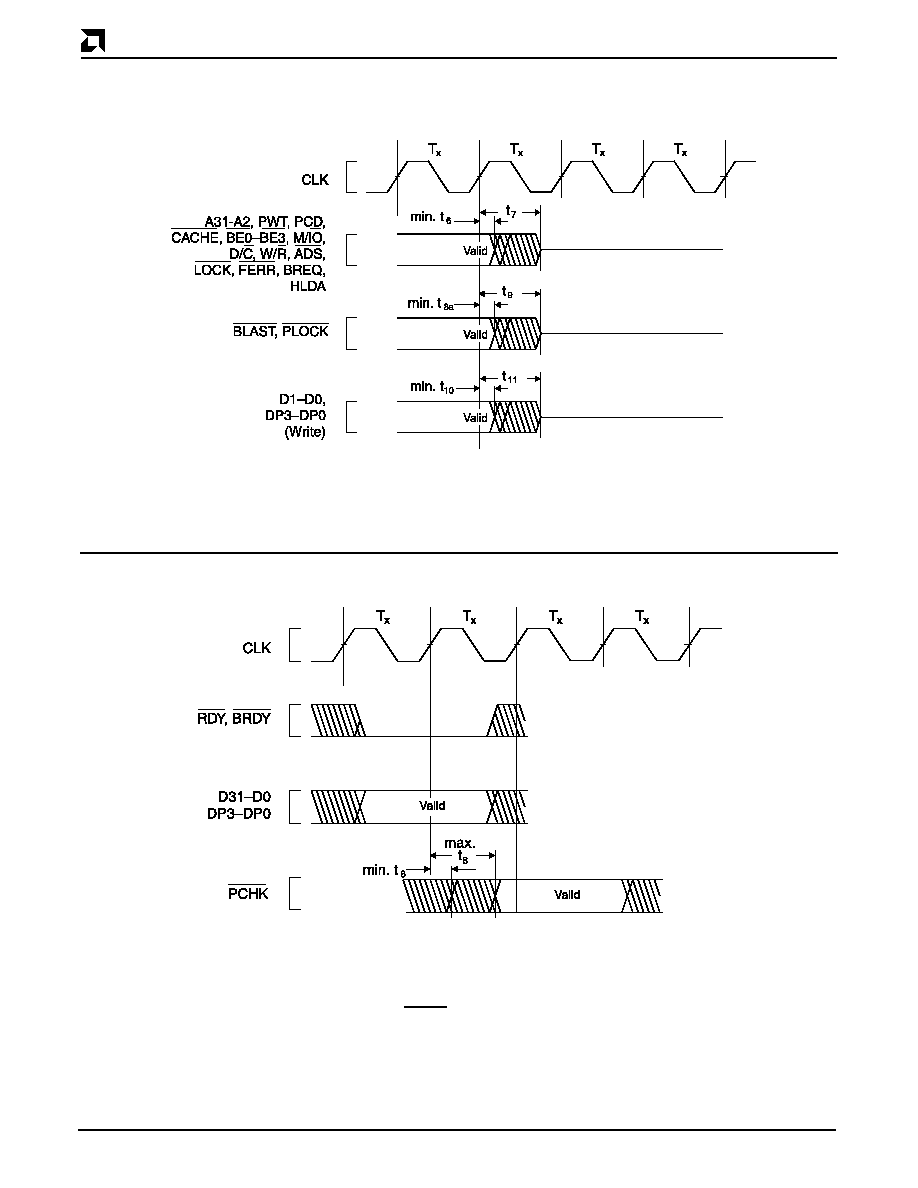
62
Am5
X
86 Microprocessor
AMD
PRELIMINARY
Figure 41. Maximum Float Delay Timing
Figure 42. PCHK Valid Delay Timing

Am5
X
86 Microprocessor
63
AMD
PRELIMINARY
Figure 43. Input Setup and Hold Timing
Figure 44. RDY and BRDY Input Setup and Hold Timing

64
Am5
X
86 Microprocessor
AMD
PRELIMINARY
Figure 45. TCK Waveforms
Figure 46. Test Signal Timing Diagram

Am5
X
86 Microprocessor
65
AMD
PRELIMINARY
12
PACKAGE THERMAL
SPECIFICATIONS
The Am5
X
86 microprocessor is specified for operation
when T
CASE
(the case temperature) is within the range
of 0
∞
C to +55
∞
C or +85
∞
C. T
CASE
can be measured in
any environment to determine whether the Am5
X
86 mi-
croprocessor is within specified operating range. The
case temperature should be measured at the center of
the top surface opposite the pins.
The ambient temperature (T
A
) is guaranteed if T
CASE
is
not violated. The ambient temperature can be calculated
from
JC
and
JA
and from the following equations:
T
J
= T
CASE
+ (P ∑
JC
)
T
A
= T
J
≠ (P ∑
JA
)
T
CASE
= T
A
+ (P ∑ [
JA
≠
JC
])
Where:
T
J
, T
A
, T
CASE
= Junction, Ambient, and Case Temperature
JC
,
JA
= Junction-to-Case and Junction-to-Ambient
Thermal Resistance, respectively
P
= Maximum Power Consumption
The values for
JA
and
JC
are given in Table 21 for the
1.75 sq. in., 168-pin, ceramic PGA. For the 208-pin
SQFP plastic package,
JA
= 14.0 and
JC
= 1.5.
Table 22 shows the T
A
allowable (without exceeding
T
CASE
) at various airflows and T
CASE
values for the PGA
package. Note that T
A
is greatly improved by attaching
a heat sink to the package. P (the maximum power con-
sumption) is calculated by using a maximum I
CC
value
of 931 mA at 3.3 V. Table 23 shows the T
A
allowable
(without exceeding T
CASE
) for the SQFP package using
a maximum I
CC
value of 931 mA at 3.3 V.
Note:
*0.350
high unidirectional heat sink (Al alloy 6063-T5, 40 mil fin width, 155 mil center-to-center fin spacing)
Table 21. Thermal Resistance (∞C/W)
JC
and
JA
for the Am5
X
86 CPU in 168-Pin PGA Package
Cooling
Mechanism
JC
JA
vs. Airflow-Linear ft/min. (m/s)
0
(0)
200
(1.01)
400
(2.03)
600
(3.04)
800
(4.06)
1000
(5.07)
No Heat Sink
1.5
16.5
14.0
12.0
10.5
9.5
9.0
Heat Sink*
2.0
12.0
7.0
5.0
4.0
3.5
3.25
Heat Sink* and fan
2.0
5.0
4.6
4.2
3.8
3.5
3.25
Table 22. Maximum T
A
at Various Airflows in
∞
C
T
A
by Cooling Type
T
CASE
Clock
Airflow-Linear ft/min. (m/sec)
0
(0)
200
(1.01)
400
(2.03)
600
(3.04)
800
(4.06)
1000
(5.07)
T
A
without Heat Sink
55
∞
C
133 MHz
8.9
∞
C
16.6
∞
C
22.7
∞
C
27.3
∞
C
30.4
∞
C
32.0
∞
C
T
A
with Heat Sink
55
∞
C
133 MHz
24.3
∞
C
39.6
∞
C
45.8
∞
C
48.9
∞
C
50.4
∞
C
51.2
∞
C
T
A
with Heat Sink and fan
55
∞
C
133 MHz
45.8
∞
C
47.0
∞
C
48.2
∞
C
49.5
∞
C
50.4
∞
C
51.2
∞
C
T
A
without Heat Sink
85
∞
C
133 MHz
38.9
∞
C
46.6
∞
C
52.7
∞
C
57.3
∞
C
60.4
∞
C
62.0
∞
C
T
A
with Heat Sink
85
∞
C
133 MHz
54.3
∞
C
69.6
∞
C
75.8
∞
C
78.9
∞
C
80.4
∞
C
81.2
∞
C
T
A
with Heat Sink and fan
85
∞
C
133 MHz
75.8
∞
C
77.0
∞
C
78.2
∞
C
79.5
∞
C
80.4
∞
C
81.2
∞
C
Table 23. Maximum T
A
for SQFP Package by Clock Frequency
T
CASE
Clock
T
A
85
∞
C
133 MHz
46.6
∞
C

66
Am5
X
86 Microprocessor
AMD
PRELIMINARY
13
PHYSICAL DIMENSIONS
1.735
1.765
1.735
1.765
Bottom View (Pins Facing Up)
Base Plane
Seating Plane
0.140
0.180
0.110
0.140
0.105
0.125
0.017
0.020
Side View
168-Pin PGA
0.025
0.045
1.595
1.605
1.595
1.605
Index
Corner
0.090
0.110
Notes:
1. All measurements are in inches.
2. Not to scale. For reference only.
3. BSC is an ANSI standard for Basic Space Centering.
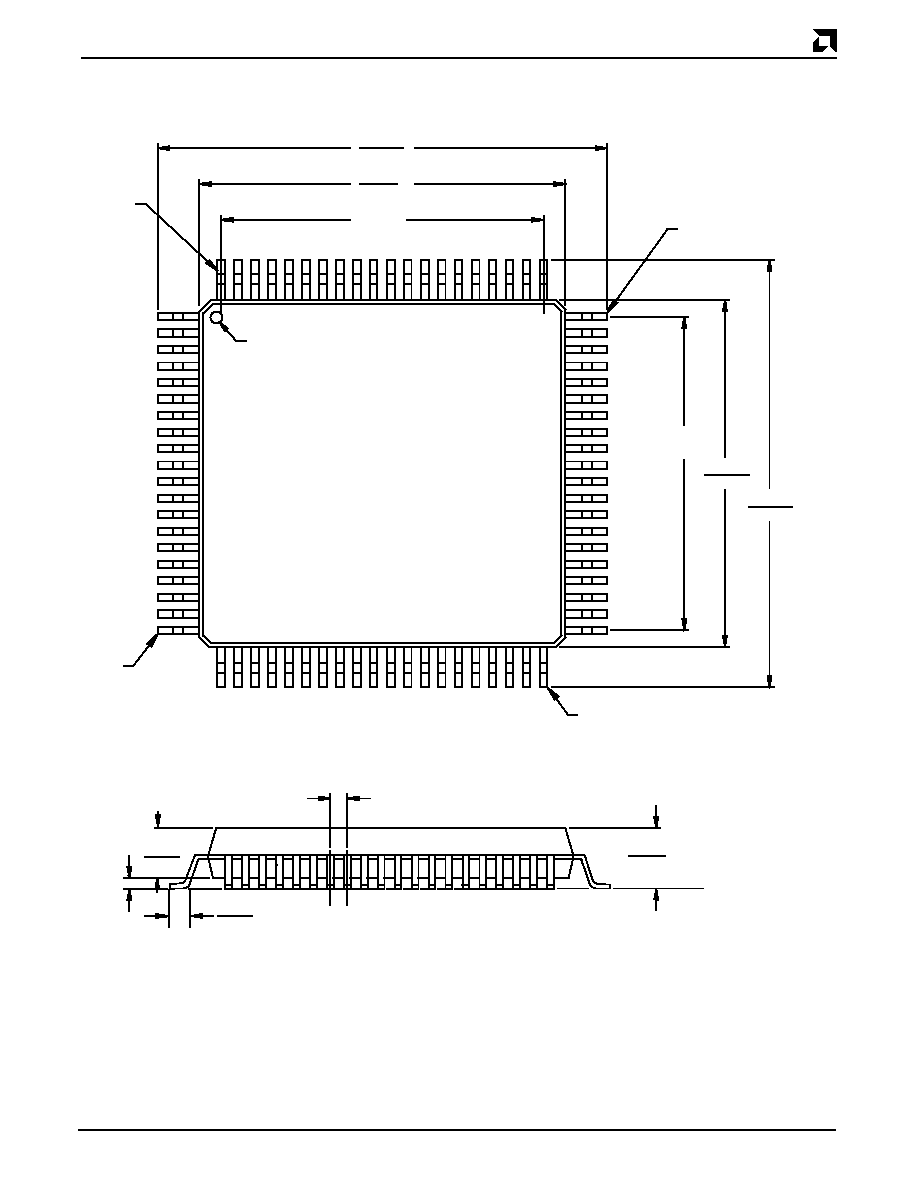
AMD
PRELIMINARY
Am5
X
86 Microprocessor
67
Notes:
1. All measurements are in millimeters unless otherwise noted.
2. Not to scale. For reference only.
30.40
30.80
27.90
28.10
25.50
REF
Pin 156
Pin 208
Pin 52
Pin 104
Pin 1 I.D.
27.90
28.10
Seating
Plane
0.50
BASIC
0.05
Min
3.25
3.45
3.70
Max.
Top View
Side View
25.50
REF
30.40
30.80
208-Pin SQFP
Trademarks
AMD, Am386, and Am486 are registered trademarks and Am5
X
86 is a trademark of Advanced Micro Devices, Inc.
FusionPC is a service mark of Advanced Micro Devices, Inc.
Microsoft and Windows are registered trademarks of Microsoft Corp.
Product names used in this publication are for identification purposes only and may be trademarks of their respective companies.
0.50
0.75