This Data Sheet states AMD's current specifications regarding the Products described herein. This Data Sheet may
be revised by subsequent versions or modifications due to changes in technical specifications.
Publication# 22142
Rev: F Amendment/+5
Issue Date: November 22, 2002
Refer to AMD's Website (www.amd.com) for the latest information.
Am29BL162C
16 Megabit (1 M x 16-Bit)
CMOS 3.0 Volt-only Burst Mode Flash Memory
DISTINCTIVE CHARACTERISTICS
32 words sequential with wrap around (linear
32), bottom boot
One 8 Kword, two 4 Kword, one 112 Kword, and
seven 128 Kword sectors
Single power supply operation
-- Regulated voltage range: 3.0 to 3.6 volt read
and write operations and for compatibility with
high performance 3.3 volt microprocessors
Read access times
Burst access times as fast as 17 ns at industrial
temperature range (18 ns at extended
temperature range)
Initial/random access times as fast as 65 ns
Alterable burst length via BAA# pin
Power dissipation (typical)
-- Burst Mode Read: 15 mA @ 25 MHz,
20 mA @ 33 MHz, 25 mA @ 40 MHz
-- Program/Erase: 20 mA
-- Standby mode, CMOS: 3 µA
5 V-tolerant data, address, and control signals
Sector Protection
-- Implemented using in-system or via
programming equipment
-- Temporary Sector Unprotect feature allows code
changes in previously locked sectors
Unlock Bypass Program Command
-- Reduces overall programming time when
issuing multiple program command sequences
Embedded Algorithms
-- Embedded Erase algorithm automatically
preprograms and erases the entire chip or any
combination of designated sectors
-- Embedded Program algorithm automatically
writes and verifies data at specified addresses
Minimum 1 million erase cycle guarantee
per sector
20-year data retention
CFI (Common Flash Interface) compliant
-- Provides device-specific information to the
system, allowing host software to easily
reconfigure for different Flash devices
Compatibility with JEDEC standards
-- Pinout and software compatible with single-
power supply Flash
-- Superior inadvertent write protection
-- Backward-compatible with AMD Am29LVxxx
and Am29Fxxx flash memories: powers up in
asynchronous mode for system boot, but can
immediately be placed into burst mode
Data# Polling and toggle bits
-- Provides a software method of detecting
program or erase operation completion
Ready/Busy# pin (RY/BY#)
-- Provides a hardware method of detecting
program or erase cycle completion
Erase Suspend/Erase Resume
-- Suspends an erase operation to read data from,
or program data to, a sector that is not being
erased, then resumes the erase operation
Hardware reset pin (RESET#)
-- Hardware method to reset the device for reading
array data
Package Option
-- 56-pin SSOP

2
Am29BL162C
November 22, 2002
GENERAL DESCRIPTION
The Am29BL162C is a 16 Mbit, 3.0 Volt-only burst
mode Flash memory devices organized as 1,048,576
words. The device is offered in a 56-pin SSOP
package. These devices are designed to be pro-
grammed in-system with the standard system 3.0-volt
V
CC
supply. A 12.0-volt V
PP
or 5.0 V
CC
is not required
for program or erase operations. The device can also
be programmed in standard EPROM programmers.
The device offers access times of 65, 70, 90, and 120
ns, allowing high speed microprocessors to operate
without wait states. To eliminate bus contention the
device has separate chip enable (CE#), write enable
(WE#) and output enable (OE#) controls.
Burst Mode Features
The Am29BL162C offers a Linear Burst mode--a
32 word sequential burst with wrap around--in a
bottom boot configuration only. This devices require
additional control pins for burst operations: Load
Burst Address (LBA#), Burst Address Advance
(BAA#), and Clock (CLK). This implementation allows
easy interface with minimal glue logic to a wide range
of microprocessors/microcontrollers for high perfor-
mance read operations.
AMD Flash Memory Features
Each device requires only a single 3.0 volt power
supply for both read and write functions. Internally
generated and regulated voltages are provided for the
program and erase operations. The I/O and control
signals are 5V tolerant.
The device is entirely command set compatible with the
JEDEC single-power-supply Flash standard. Com-
mands are written to the command register using stan-
dard microprocessor write timings. Register contents
serve as input to an internal state-machine that con-
trols the erase and programming circuitry. Write cycles
also internally latch addresses and data needed for the
programming and erase operations. Reading data out
of the device is similar to reading from other Flash or
EPROM devices.
Device erasure occurs by executing the erase com-
mand sequence. This initiates the Embedded Erase
algorithm--an internal algorithm that automatically pre-
programs the array (if it is not already programmed) be-
fore executing the erase operation. During erase, the
device automatically times the erase pulse widths and
verifies proper cell margin.
The host system can detect whether a program or
erase operation is complete by observing the RY/BY#
pin, or by reading the DQ7 (Data# Polling) and DQ6
(toggle) status bits. After a program or erase cycle
has been completed, the device is ready to read array
data or accept another command.
The sector erase architecture allows memory sectors
to be erased and reprogrammed without affecting the
data contents of other sectors. The device is fully
erased when shipped from the factory.
Hardware data protection measures include a low V
CC
detector that automatically inhibits write operations dur-
ing power transitions. The hardware sector protection
feature disables both program and erase operations in
any combination of the sectors of memory. This can be
achieved in-system or via programming equipment.
The Erase Suspend/Erase Resume feature enables
the user to put erase on hold for any period of time to
read data from, or program data to, any sector that is
not selected for erasure. True background erase can
thus be achieved.
The hardware RESET# pin terminates any operation
in progress and resets the internal state machine to
reading array data. The RESET# pin may be tied to the
system reset circuitry. A system reset would thus also
reset the device, enabling the system microprocessor
to read the boot-up firmware from the Flash memory.
The device offers two power-saving features. When
addresses have been stable for a specified amount of
time, the device enters the automatic sleep mode.
The system can also place the device into the standby
mode. Power consumption is greatly reduced in both
these modes.
AMD's Flash technology combines years of Flash
memory manufacturing experience to produce the
highest levels of quality, reliability and cost effectiveness.
The device electrically erases all bits within a sector
simultaneously via Fowler-Nordheim tunneling. The
data is programmed using hot electron injection.

November 22, 2002
Am29BL162C
3
TABLE OF CONTENTS
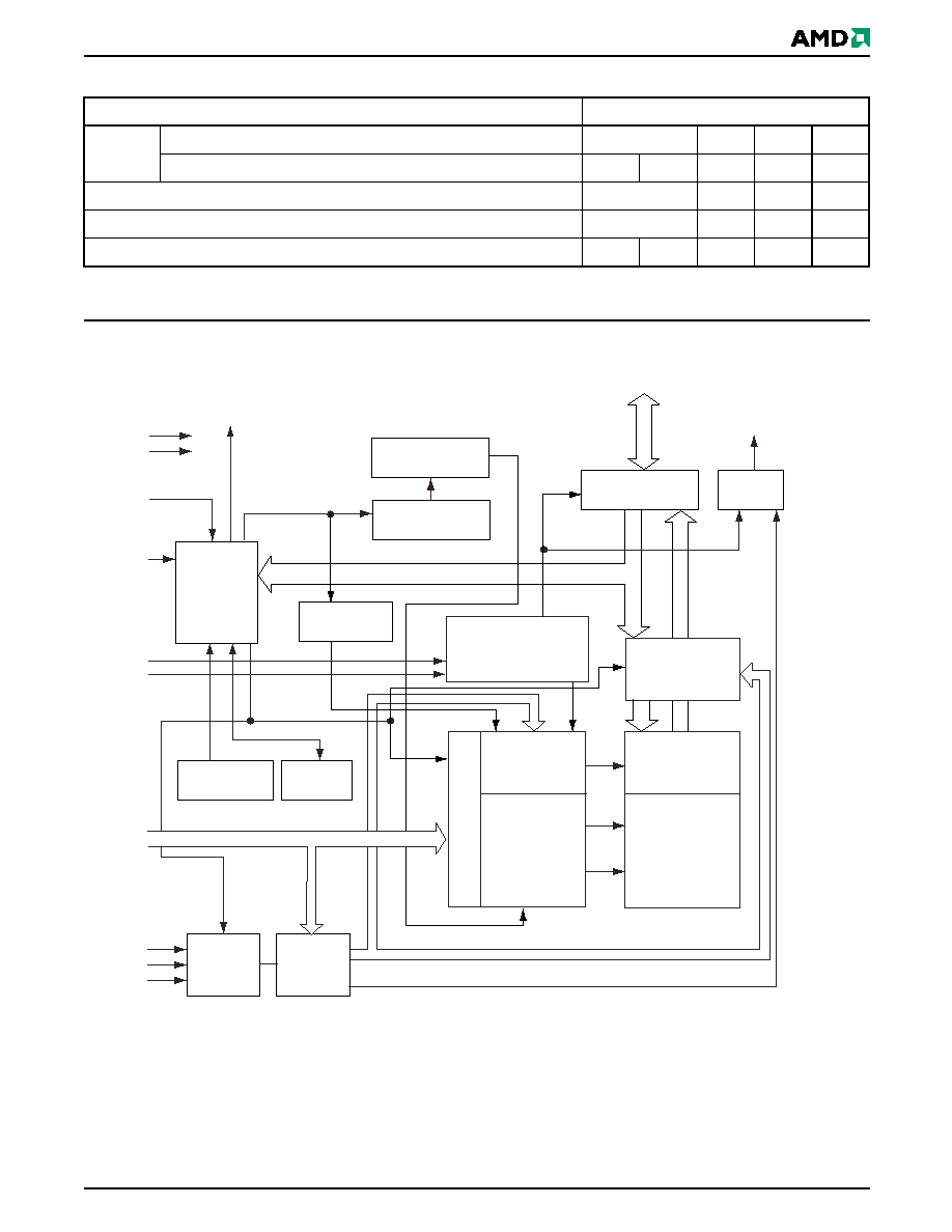
Product Selector Guide . . . . . . . . . . . . . . . . . . . . . 5
Block Diagram . . . . . . . . . . . . . . . . . . . . . . . . . . . . 5
Connection Diagrams . . . . . . . . . . . . . . . . . . . . . . 6
Pin Configuration . . . . . . . . . . . . . . . . . . . . . . . . . . 7
Ordering Information . . . . . . . . . . . . . . . . . . . . . . . 8
Device Bus Operations . . . . . . . . . . . . . . . . . . . . . . 9
Table 1. Device Bus Operations .......................................................9
Requirements for Reading Array Data Array in Asynchronous
(Non-Burst) Mode ................................................................... 10
Requirements for Reading Array Data in Synchronous
(Burst) Mode ........................................................................... 10
Burst Suspend/Burst Resume Operations.............................. 11
IND# End of Burst Indicator .................................................... 11
Writing Commands/Command Sequences ............................ 11
Program and Erase Operation Status .................................... 11
Standby Mode ........................................................................ 11
Automatic Sleep Mode ........................................................... 11
RESET#: Hardware Reset Pin ............................................... 11
Output Disable Mode .............................................................. 12
Table 2. Sector Address Table ........................................................12
Autoselect Mode..................................................................... 13
Table 3. Am29BL162C Autoselect Codes (High Voltage Method) ..13
Sector Protection/Unprotection ............................................... 13
Figure 1. In-System Sector Protect/Unprotect Algorithms .............. 14
Temporary Sector Unprotect .................................................. 15
Figure 2. Temporary Sector Unprotect Operation........................... 15
Hardware Data Protection . . . . . . . . . . . . . . . . . . 15
Low V
CC
Write Inhibit .............................................................. 15
Write Pulse "Glitch" Protection ............................................... 15
Logical Inhibit .......................................................................... 15
Power-Up Write Inhibit ............................................................ 15
Common Flash Memory Interface (CFI) . . . . . . . 16
Table 4. CFI Query Identification String ..........................................16
Table 5. System Interface String .....................................................16
Table 6. Device Geometry Definition ..............................................17
Table 7. Primary Vendor-Specific Extended Query ........................17
Command Definitions . . . . . . . . . . . . . . . . . . . . . 18
Reading Array Data in Non-burst Mode ................................. 18
Reading Array Data in Burst Mode ......................................... 18
Figure 3. Burst Mode Read with 40 MHz CLK, 65 ns
t
IACC
, 18 ns t
BACC
Parameters....................................................... 19
Figure 4. Burst Mode Read with 25 MHz CLK, 70 ns
t
IACC
, 24 ns t
BACC
Parameters....................................................... 19
Reset Command ..................................................................... 19
Autoselect Command Sequence ............................................ 19
Program Command Sequence ............................................... 20
Unlock Bypass Command Sequence ..................................... 20
Figure 5. Program Operation .......................................................... 21
Chip Erase Command Sequence ........................................... 21
Sector Erase Command Sequence ........................................ 21
Figure 6. Erase Operation............................................................... 22
Erase Suspend/Erase Resume Commands ........................... 22
Asynchronous Mode ............................................................... 22
Burst Mode ............................................................................. 22
General ................................................................................... 22
Command Definitions ............................................................. 24
Table 8. Am29BL162C Command Definitions ............................... 24
Write Operation Status . . . . . . . . . . . . . . . . . . . . 25
DQ7: Data# Polling ................................................................. 25
Figure 7. Data# Polling Algorithm .................................................. 25
RY/BY#: Ready/Busy# ............................................................ 26
DQ6: Toggle Bit I .................................................................... 26
DQ2: Toggle Bit II ................................................................... 26
Reading Toggle Bits DQ6/DQ2 ............................................... 26
DQ5: Exceeded Timing Limits ................................................ 27
DQ3: Sector Erase Timer ....................................................... 27
Figure 8. Toggle Bit Algorithm........................................................ 27
Table 9. Write Operation Status ..................................................... 28
Absolute Maximum Ratings . . . . . . . . . . . . . . . . 29
Operating Ranges . . . . . . . . . . . . . . . . . . . . . . . . . 29
DC Characteristics . . . . . . . . . . . . . . . . . . . . . . . . 30
Figure 11. I
CC1
Current vs. Time (Showing Active and Automatic
Sleep Currents) .............................................................................. 31
Figure 12. Typical I
CC1
vs. Frequency ........................................... 31
Test Conditions . . . . . . . . . . . . . . . . . . . . . . . . . . 32
Figure 13. Test Setup..................................................................... 32
Table 10. Test Specifications ......................................................... 32
Key to Switching Waveforms .................................................. 32
Figure 14. Input Waveforms and Measurement Levels ................. 32
AC Characteristics . . . . . . . . . . . . . . . . . . . . . . . . 33
Figure 15. Conventional Read Operations Timings ....................... 35
Figure 16. Burst Mode Read .......................................................... 35
Hardware Reset (RESET#) .................................................... 36
Figure 17. RESET# Timings .......................................................... 36
Erase/Program Operations ..................................................... 37
Figure 18. Program Operation Timings.......................................... 38
Figure 19. Chip/Sector Erase Operation Timings .......................... 39
Figure 20. Data# Polling Timings (During Embedded Algorithms). 40
Figure 21. Toggle Bit Timings (During Embedded Algorithms)...... 40
Figure 22. DQ2 vs. DQ6 for Erase and
Erase Suspend Operations ............................................................ 41
Figure 23. Temporary Sector Unprotect Timing Diagram .............. 41
Figure 24. Sector Protect/Unprotect Timing Diagram .................... 42
Alternate CE# Controlled Erase/Program Operations ............ 43
Figure 25. Alternate CE# Controlled Write Operation Timings ...... 44
Erase and Programming Performance . . . . . . . 45
Latchup Characteristics . . . . . . . . . . . . . . . . . . . . 45
SSOP Pin Capacitance . . . . . . . . . . . . . . . . . . . . . 45
Data Retention. . . . . . . . . . . . . . . . . . . . . . . . . . . . 45
Physical Dimensions . . . . . . . . . . . . . . . . . . . . . . 46
SSO056--56-Pin Shrink Small Outline Package .................... 46
Revision Summary . . . . . . . . . . . . . . . . . . . . . . . . 47
Revision A (September 1998) ................................................. 47
Revision B (December 1998) .................................................. 47
Revision C (December 1998) ................................................. 47
Revision D (May 17, 1999) ..................................................... 47
Revision D+1 (July 2, 1999) ................................................... 47
Revision E (November 2, 1999) .............................................. 47
Revision F (June 20, 2000) ..................................................... 48
Revision F+1 (November 21, 2000) ........................................ 48
Revision F+2 (July 22, 2002) .................................................. 48
Revision F+3 (August 19, 2002) ............................................. 48