Altera Corporation
1
November 2002, ver. 1.1
Data Sheet
DS-A6402-1.1
Features
Optimized for the Stratix
TM
GX, Cyclone
TM
, Stratix, APEX
Æ
, APEX II,
and FLEX
Æ
device families
Uses approximately 162 logic elements (LEs)
Programmable word length, stop bits, and parity
Full duplex operation
Includes status flags for parity, framing, and overrun errors
Functionally based on the Harris HD-6402 device, except as noted in
the
"Variations & Clarifications" on page 8
General
Description
The a6402 function implements a universal asynchronous
receiver/transmitter (UART), which provides an interface between a
microprocessor and a serial communications channel.
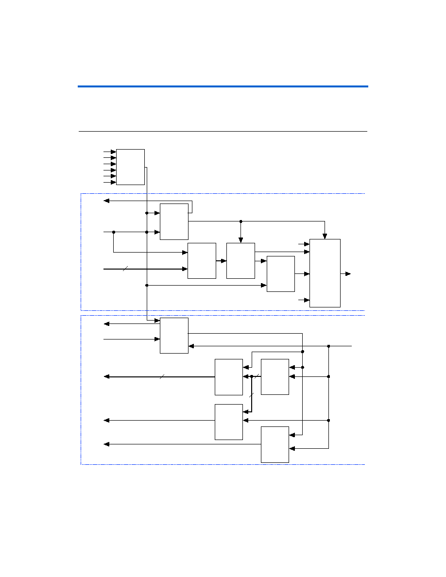
Figure 1
shows the
a6402 symbol.
Figure 1. a6402 Symbol
cls1
cls2
crl
ndrr
epe
mr
pi
rrc
rri
sbs
ntbrl
tbr[7..0]
trc
dr
fe
oe
pe
rbr[7..0]
tbre
tre
tro
A6402
en_tx
en_rx
a6402
Universal Asynchronous
Receiver/Transmitter

2
Altera Corporation
a6402 Universal Asynchronous Receiver/Transmitter Data Sheet
Signals
Table 1
shows the input and output signals for the a6402.
Table 1. a6402 Signals (Part 1 of 2)
Name
Type
Polarity
Description
en_rx
en_tx
Input
High
Clock enables. The en_rx and en_tx signals allow the UART to remain
fully synchronous with the system high-speed clock, while operating at the
receive and transmit enable frequencies. The en_rx and en_tx signals are
pulses that are high for one system clock period and are at a rate 16 times
the rate of the desired receive and transmit data rates.
cls1
cls2
Input
≠
Character length select bits. These bits determine the length of the data
word.
00 = 5-bit word format
01 = 6-bit word format
10 = 7-bit word format
11 = 8-bit word format
crl
Input
High
Control register load. Controls how the data word is loaded into the control
register.
ndrr
Input
Low
Data received reset. Clears the dr output.
epe
Input
High/low Even parity enable. When high, even parity; when low, odd parity.
mr
Input
High
Master reset. Clears the pe, fe, dr, and oe outputs, and asserts the tre
and tbre outputs.
pi
Input
High
Parity inhibit. When pi is asserted, parity is neither generated nor checked.
rrc
Input
≠
Receiver register clock. Operates at 16 times the receive data rate.
rri
Input
≠
Receiver register input. Serial input data.
sbs
Input
High/low Stop bit select. When high, sbs generates 2 stop bits (1.5 stop bits for 5-bit
format); when low, sbs
generates 1 stop bit.
ntbr1
Input
Low
Transmitter buffer register load. Enables load of the transmitter buffer
register.
tbr[7:0]
Input
≠
Transmitter buffer register input bus.
trc
Output
≠
Transmitter register clock. Operates at 16 times the transmit data rate.
dr
Output
High
Data received. Indicates that a data word has been transferred to the
receiver buffer register.
fe
Output
High
Framing error. Asserted when the expected stop bit(s) is not detected.
oe
Output
High
Overrun error. Asserted when data in the receiver buffer register is
overwritten while the dr output is still asserted.
pe
Output
High/low Parity error. Set when the calculated parity does not match the received
parity. When pi is asserted, pe is set low.
rbr[7:0]
Output
≠
Receiver buffer register bus.
tbre
Output
High
Transmitter buffer register empty. Indicates that the transmitter buffer
register is empty.
Altera Corporation
3
a6402 Universal Asynchronous Receiver/Transmitter Data Sheet
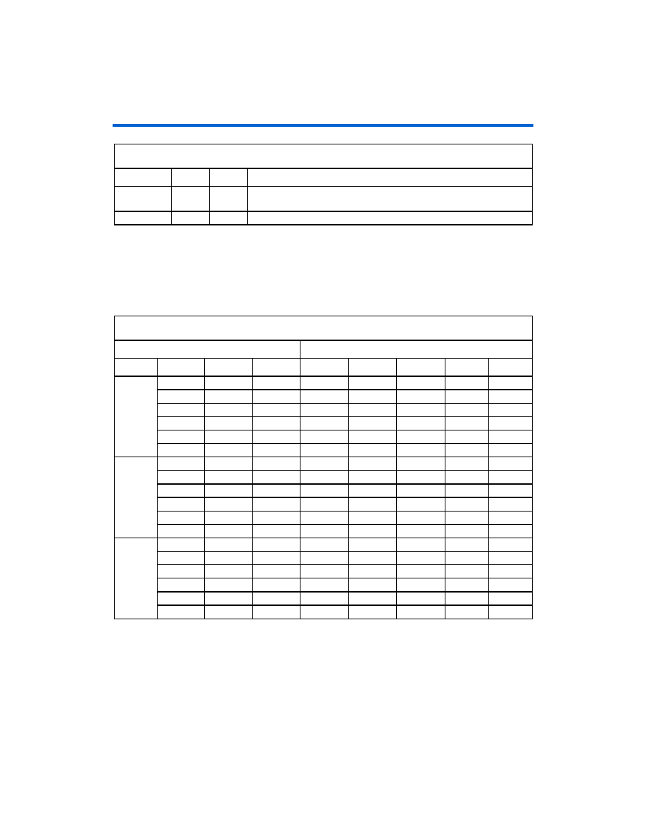
Configurations
The a6402 receives and transmits data in a variety of configurations,
including 5-, 6-, 7-, or 8-bit data words; odd, even, or no parity; and 1, 1.5,
or 2 stop bits. Table 2 shows the available configuration options.
tre
Output
High
Transmitter register empty. Indicates that the data word is completely
transmitted out of the transmitter register.
tro
Output
≠
Transmitter register output. Serial output data.
Table 1. a6402 Signals (Part 2 of 2)
Name
Type
Polarity
Description
Table 2. a6402 Available Configurations (Part 1 of 2)
Character Format
Control Word
Data bits
Parity Bit
Start Bit
Stop Bits
cls2
cls1
pi
epe
(1)
sbs
5
Odd
1
1
0
0
0
0
0
Odd
1
1.5
0
0
0
0
1
Even
1
1
0
0
0
1
0
Even
1
1.5
0
0
0
1
1
None
1
1
0
0
1
X
0
None
1
1.5
0
0
1
X
1
6
Odd
1
1
0
1
0
0
0
Odd
1
2
0
1
0
0
1
Even
1
1
0
1
0
1
0
Even
1
2
0
1
0
1
1
None
1
1
0
1
1
X
0
None
1
2
0
1
1
X
1
7
Odd
1
1
1
0
0
0
0
Odd
1
2
1
0
0
0
1
Even
1
1
1
0
0
1
0
Even
1
2
1
0
0
1
1
None
1
1
1
0
1
X
0
None
1
2
1
0
1
X
1