 | ÐлекÑÑоннÑй компоненÑ: A8436 | СкаÑаÑÑ:  PDF PDF  ZIP ZIP |
Äîêóìåíòàöèÿ è îïèñàíèÿ www.docs.chipfind.ru
A8436-DS, Rev. 2
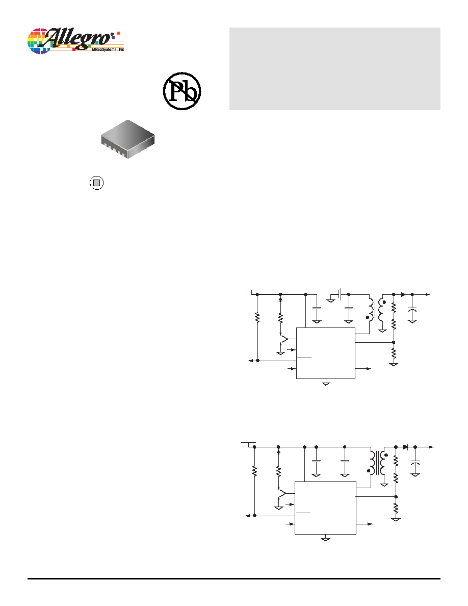
The A8436 is a highly integrated IC that charges
photoflash capacitors for digital and film cameras. It
also features an integrated IGBT driver that facilitates
the flash discharge function and saves board space.
To charge the photoflash capacitor, the A8436
integrates a 40 V, DMOS switch that drives the trans-
former in a flyback topology, allowing optimized
design with tight coupling and high efficiency. A pro-
prietary control scheme optimizes the capacitor charg-
ing time. Low quiescent current and low shutdown
current further improve system efficiency and extend
battery life.
Three levels of switch current limit are provided:
1.0, 1.2, and 1.4 A. The level is determined by config-
uring the ILIM pin as grounded, floating, or pulled up
to IC supply voltage, respectively.
The CHARGE pin enables the A8436 and starts the
charging of the output capacitor. When the designated
output voltage is reached, the A8436 stops the charg-
ing until the CHARGE pin is toggled again. Pulling
the CHARGE pin low stops charging. The ¯D¯ ¯O¯ ¯N¯ ¯E¯ pin
is an open-drain indicator of when the designated out-
put voltage is reached.
The A8436 can be used with two Alkaline/NiMH/
NiCAD or one single-cell Li+ battery connected to the
transformer primary. Connect the VIN pin to a 3.0 to
5.5 V supply, which can be either the system rail or the
Li+ battery, if used.
The A8436 is available in a very low profile
(0.75 mm) 10-terminal 3×3 mm MLP/TDFN package,
making it ideal for space-constrained applications. It is
lead (Pb) free, with 100% matte-tin leadframe plating.
Photoflash Capacitor
Charger with IGBT Driver
A8436
Package EJ:
MLP/TDFN, 3 × 3 mm
0.75 mm Nominal Height
FEATURES
APPLICATIONS
Power with 1 Li+ or 2 Alkaline/NiMH/NiCAD batteries
Adjustable output voltage
>75% efficiency
Three levels of switch current limit: 1.0, 1.2, 1.4 A
Fast charge time
Charge complete indication
Integrated IGBT driver with trigger
No primary-side Schottky diode needed
Low-profile package (0.75 mm nominal height)
Digital camera flash
Film camera flash
Cell phone flash
Emergency strobe light
Approximate Scale 1:1
Figure 1. Typical circuit with separate power supply to transformer
Figure 2. Typical circuit with single power supply
To IGBT Gate
k
COUT
V
OUT
D1
T1
R1
R2
R3
R4
100 k
R5
10
One Li+ battery
or 3.0 to 5.5 V
V
BATT
C2
4.7 F
C1
0.1 F
1.4 A
1.2 A (N.C.)
1.0 A
A8436
CHARGE
GND
FB
SW
TRIGGER
IGBTDRV
DONE
ILIM
VIN
1.4 A
1.2 A (N.C.)
1.0 A
+
To IGBT Gate
k
COUT
V
OUT
D1
T1
R1
R2
R3
R4
100 k
R5
10
V
BATT
Two Alkaline/NiMH/NiCAD or one Li+ battery
or 1.5 to 5.5 V
V
BIAS
3.0 to 5.5 V
C2
4.7 F
C1
0.1 F
A8436
CHARGE
GND
FB
SW
TRIGGER
IGBTDRV
DONE
ILIM
VIN
A8436-DS, Rev. 2
Worcester, Massachusetts 01615-0036 (508) 853-5000
115 Northeast Cutoff, Box 15036
www.allegromicro.com
Allegro MicroSystems, Inc.
Photoflash Capacitor Charger with IGBT Driver
A8436
2
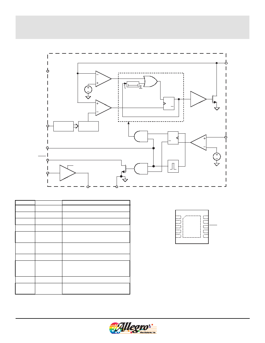
Functional Block Diagram
VIN
VIN
SW
CHARGE
GND
CMP2
ILIM
DONE
FB
Q
I
LIM
Decoder
Adjustable
Reference
IGBTDRV
TRIGGER
1.2 V
40 V
DMOS
Q
Q
SET
CLR
S
R
Q
Q
SET
CLR
S
R
CMP3
CMP1
1.2 V
I
LIM
Comparator
DCM
Comparator
H L
Triggered Timer
Control Logic
Enable
18 s
One-Shot
Terminal List Table
Ab so lute Max i mum Rat ings
10
9
8
7
6
ILIM
FB
DONE
TRIGGER
SW
1
2
3
4
5
NC
IGBTDRV
VIN
GND
CHARGE
Device Pin-out Diagram
R
JA
= 45 °C/W, on a 4-layer board. Additional information is
available on the Allegro Web site.
Package Thermal Characteristics
Number
Name
Function
1
NC
No connection
2
IGBTDRV
IGBT driver gate drive output
3
VIN
Power supply input
4
GND
Device ground
5
CHARGE
Charging enable; set to low to power-
off the A8436
6
SW
Switch, internally connected to the
DMOS power FET drain
7
TRIGGER
Strobe signal input
8
¯D¯ ¯O¯ ¯N¯ ¯E¯
Open drain, when pulled low by inter-
nal MOSFET, indicates that charging
target level has been reached
9
FB
Output voltage feedback
10
ILIM
Switch current limit setting; sets three
discreet levels
Input or Output Voltage
SW
pin,
V
SW
............................................................ 0.3 to 40 V
IGBTDRV
pin,
V
IGBTDRV
.............................. 0.3 to V
IN
+ 0.3 V
FB
pin,
V
FB
............................................................... 0.3 to V
IN
All other pins, V
x
...................................................... 0.3 to 7 V
Operating Ambient Temperature, T
A
................................ 40°C to 85°C
Maximum Junction Temperature, T
J(max)
........................................ 150°C
Storage Temperature, T
S
.............................................. 55°C to 150°C
A8436-DS, Rev. 2
Worcester, Massachusetts 01615-0036 (508) 853-5000
115 Northeast Cutoff, Box 15036
www.allegromicro.com
Allegro MicroSystems, Inc.
Photoflash Capacitor Charger with IGBT Driver
A8436
3
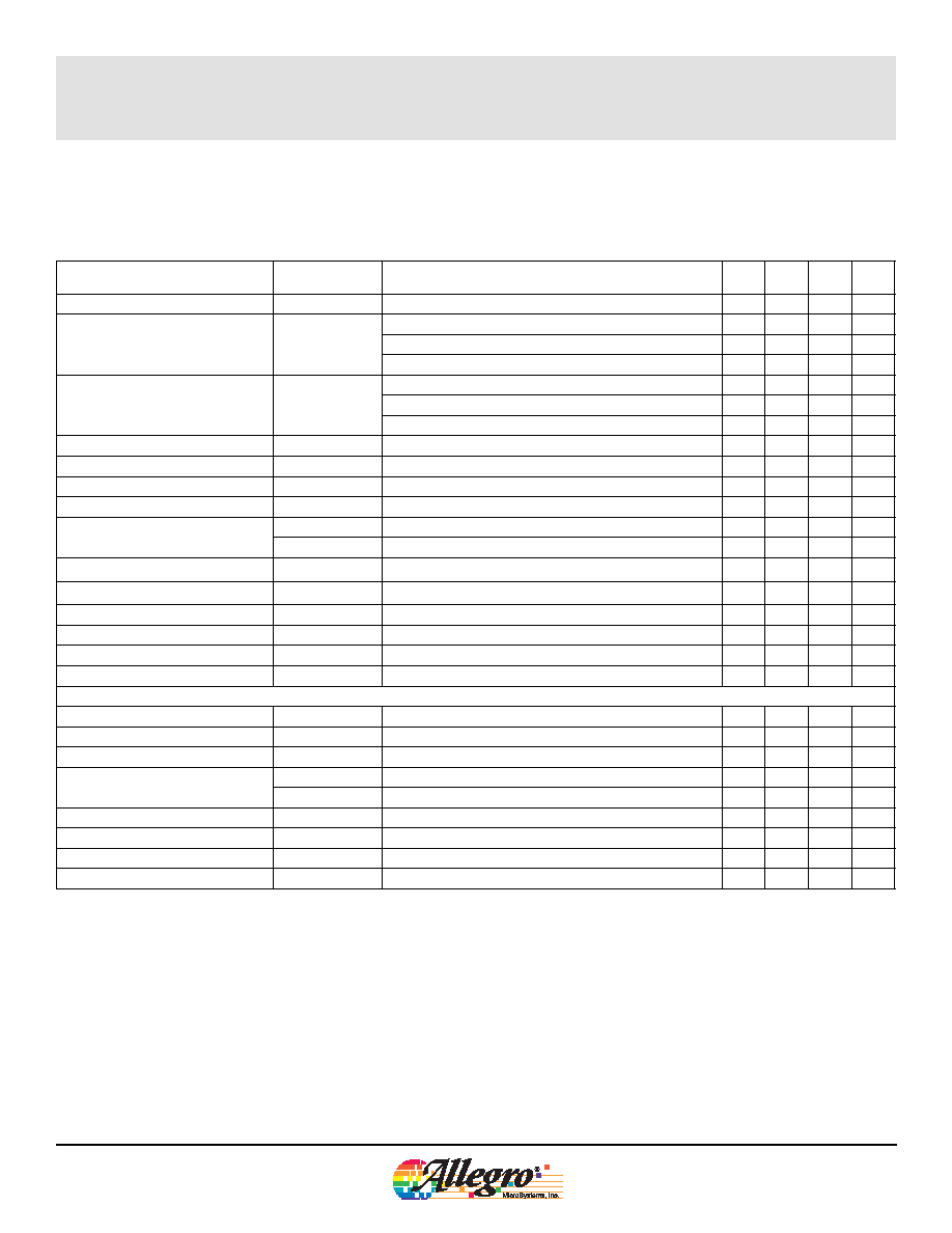
ELECTRICAL CHARACTERISTICS
Typical values at T
A
= 25°C and V
IN
= 3.3 V (unless otherwise noted)
Characteristics
Symbol
Test Conditions
Min.
Typ. Max. Units
Supply Voltage*
V
IN
3
5.5
V
Supply Current
I
IN
Charging
5
mA
Charging done
1
10
A
Shutdown (V
CHARGE
= 0 V, V
TRIGGER
= 0 V)
0.01
1
A
Primary Side Current Limit
I
SWLIM
V
ILIM
= 0 V
1.0
A
ILIM pin floating
1.08
1.2
1.32
A
V
ILIM
= V
IN
1.4
A
SW On Resistance
R
DS(On)SW
V
IN
= 3.3 V, I
D
= 800 mA, T
A
= 25°C
0.27
SW Leakage Current*
I
SWLKG
V
SW
= 35 V
1
A
SW Maximum Off-Time
t
OFF(Max)
18
s
CHARGE Input Current
I
CHARGE
V
CHARGE
= V
IN
1
A
CHARGE Input Voltage*
V
CHARGE(H)
2
V
V
CHARGE(L)
0.8
V
¯D¯ ¯O¯ ¯N¯ ¯E¯ Output Leakage Current*
I
DONELKG
1
A
¯D¯ ¯O¯ ¯N¯ ¯E¯ Output Low Voltage*
V
DONE(L)
32 A into ¯D¯ ¯O¯ ¯N¯ ¯E¯ pin
100
mV
FB Voltage Threshold*
V
FB
1.187 1.205 1.223
V
FB Input Current
I
FB
V
FB
= 1.205 V
120
nA
UVLO Enable Threshold
V
UVLO
V
IN
rising
2.55
2.65
2.75
V
UVLO Hysteresis
V
UVLOHYS
150
mV
IGBT Driver
IGBTDRV On Resistance to VIN
R
DS(On)I-V
V
IN
= 3.3 V, V
IGBTDRV
= 1.5 V
5
IGBTDRV On Resistance to GND
R
DS(On)I-G
V
IN
= 3.3 V, V
IGBTDRV
= 1.5 V
6
TRIGGER Input Current
I
TRIGGER
V
TRIGGER
= V
IN
1
A
TRIGGER Input Voltage*
V
TRIGGER(H)
2
V
V
TRIGGER(L)
0.8
V
Propagation Delay, Rising
t
Dr
R
gate
=12 , C
LOAD
= 6500 pF, V
IN
= 3.3 V
30
ns
Propagation Delay, Falling
t
Df
R
gate
=12 , C
LOAD
= 6500 pF, V
IN
= 3.3 V
30
ns
Output Rise Time
t
r
R
gate
=12 , C
LOAD
= 6500 pF, V
IN
= 3.3 V
70
ns
Output Fall Time
t
f
R
gate
=12 , C
LOAD
= 6500 pF, V
IN
= 3.3 V
70
ns
*Guaranteed by design and characterization over operating temperature range, 40°C to 85°C.
A8436-DS, Rev. 2
Worcester, Massachusetts 01615-0036 (508) 853-5000
115 Northeast Cutoff, Box 15036
www.allegromicro.com
Allegro MicroSystems, Inc.
Photoflash Capacitor Charger with IGBT Driver
A8436
4
Performance Characteristics
Tests performed using application circuit shown in figure 6 (unless otherwise noted)
Charging Waveforms
Symbol
Parameter Units/Division
C1
V
OUT
50 V
C4
I
BATT(Avg)
200 mA
t
time
1 s
Conditions
Parameter
Value
V
BATT
2.5 V
V
BIAS
3.3 V
C
OUT
100 F
Symbol
Parameter Units/Division
C1
V
OUT
50 V
C4
I
BATT(Avg)
200 mA
t
time
1 s
Conditions
Parameter
Value
V
BATT
3.6 V
V
BIAS
3.3 V
C
OUT
100 F
Symbol
Parameter Units/Division
C1
V
OUT
50 V
C4
I
BATT(Avg)
200 mA
t
time
1 s
Conditions
Parameter
Value
V
BATT
4.2 V
V
BIAS
3.3 V
C
OUT
100 F
t
I
BATT
V
OUT
C4
C1
t
I
BATT
V
OUT
C4
C1
t
I
BATT
V
OUT
C4
C1
A8436-DS, Rev. 2
Worcester, Massachusetts 01615-0036 (508) 853-5000
115 Northeast Cutoff, Box 15036
www.allegromicro.com
Allegro MicroSystems, Inc.
Photoflash Capacitor Charger with IGBT Driver
A8436
5
V
OUT
(V)
Efficiency (%)
V
BATT
(V)
Charge T
ime (s)
100
150
200
250
300
350
40
50
60
80
70
90
2.0
2.5
3.0
3.5
4.0
4.5
5.0
V
OUT
= 300 V
V
OUT
= 320 V
5.5
6.0
V
BATT
= 4.2 V
V
BATT
= 5.0 V
2
4
3
5
7
6
8
V
BATT
= 3.0 V
2
3
4
5
6
7
8
2
2.5
3
3.5
4
4.5
5
5.5
6
V
BATT
(V)
C
h
a
r
ge
Tim
e
(
s
)
V
OUT
= 300 V
V
OUT
= 320 V
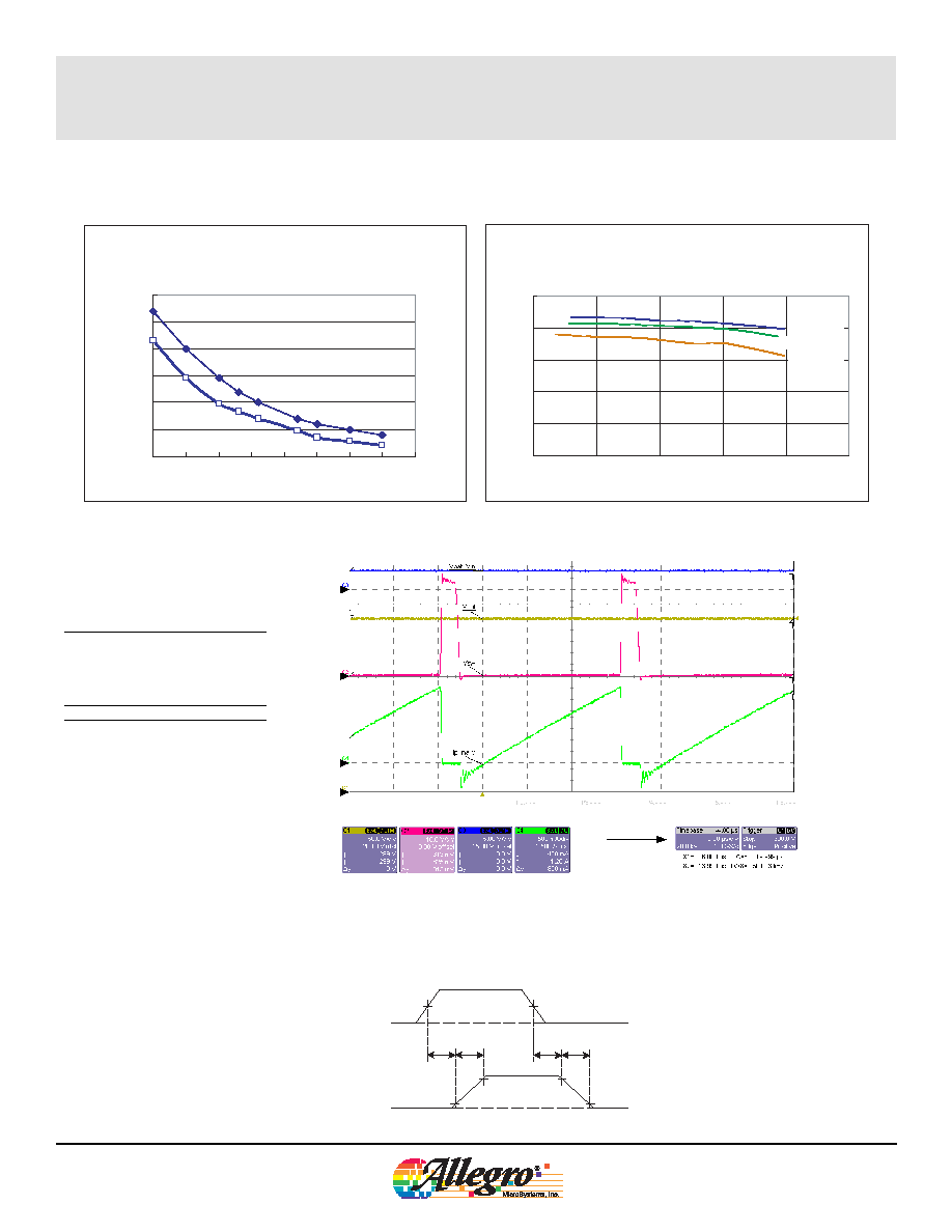
Charge Time
V
BIAS
= 3.3 V, C
OUT
= 100 F
Connect VBATT to a separate power supply
Efficiency
V
BATT
= V
BIAS
, T
A
= 25°C
Typical Switching Waveform
Performance Characteristics, continued
Tests performed using application circuit shown in figure 6 (unless otherwise noted)
IGBTDRV
TRIGGER
t
Dr
t
r
t
Df
t
f
50%
10%
90%
50%
10%
90%
IGBT Drive Timing Definition
Symbol
Parameter Units/Division
C1
V
OUT
50 V
C2
V
SW
10 V
C3
V
BATT
5 V
C4
I
Primary
500 mA
t
time
2 s
Conditions
Parameter
Value
V
OUT
300 V
V
BATT
V
IN
t
V
BATT
V
OUT
C4
C1
C3
C2
V
SW
I
Primary