
SERIAL PORT
6-BIT DAC
& LOGIC
24
23
22
21
20
19
18
17
16
15
14
13
GROUND
GROUND
SLEEP
V
REG
OUT
2B
LOAD
SUPPLY
2
SENSE
2
OUT
2A
LOGIC
SUPPLY
MUX
REF
V
DD
Dwg. PP-069-3
1
2
3
4
5
6
7
8
9
12
11
10
9
GROUND
GROUND
VCP
CP1
CP2
OUT
1B
OUT
1A
STROBE
CLOCK
DATA
SENSE
1
LOAD
SUPPLY
1
CHARGE
PUMP
OSC
V
BB2
V
BB1
6-BIT DAC
& LOGIC
Data Sheet
29319.34
3973
DUAL DMOS FULL-BRIDGE MICRO-
STEPPING PWM MOTOR DRIVER
Designed for pulse-width modulated (PWM) current control of
bipolar microstepping stepper motors, the A3973SB and A3973SLB are
capable of continuous output currents to
�1 A and operating voltages to
35 V. Internal fixed off-time PWM current-control timing circuitry can
be programmed via a serial interface to operate in slow, fast, and mixed
current-decay modes. The A3973SB (DIP) and the A3973SLB (SOIC)
are electrically identical and differ only in package style.
The desired load-current level is set via the serial port with two 6-bit
linear DACs in conjunction with a reference voltage. The six bits of
control allow maximum flexibility in torque control for a variety of step
methods, from microstepping to full-step drive. Load current is set in
1.56% increments of the maximum value.
Synchronous rectification circuitry allows the load current to flow
through the low
r
DS(on)
of the DMOS output driver during the current
decay. This feature will eliminate the need for external clamp diodes in
most applications, saving cost and external component count, while
minimizing power dissipation.
Internal circuit protection includes thermal shutdown with hyster-
esis, transient-suppression diodes, and crossover-current protection.
Special power-up sequencing is not required.
The A3973SB is supplied in a 24-lead plastic DIP with a copper
batwing power tab; the A3973SLB is supplied in a 24-lead plastic SOIC
with a copper batwing power tab for surface-mount applications. The
power tabs are at ground potential and need no electrical isolation.
FEATURES
I �1 A, 35 V Continuous Output Rating
I Low
r
DS(on)
DMOS Output Drivers
I Optimized Microstepping via 6-Bit Linear DACs
I Programmable Mixed, Fast, and Slow Current-Decay Modes
I 4 MHz Internal Oscillator for Digital Timing
I Serial-Interface Controls Chip Functions
I Synchronous Rectification for Low Power Dissipation
I Internal UVLO and Thermal Shutdown Circuitry
I Crossover-Current Protection
I Precision 2 V Reference
I Inputs Compatible with 3.3 V or 5 V Control Signals
I Sleep and Idle Modes
PRELIMINARY INFORMATION
(Subject to change without notice)
December 1, 2000
ABSOLUTE MAXIMUM RATINGS
at T
A
= +25
�C
Load Supply Voltage, V
BB
................ 35 V
Output Current, I
OUT
......................
�1.0 A
Logic Supply Voltage, V
DD
.............. 7.0 V
Logic Input Voltage Range,
V
IN
................ -0.3 V to V
DD
+ 0.3 V
Reference Voltage, V
REF
..................... 3 V
Sense Voltage (dc), V
S
................ 500 mV
Package Power Dissipation, P
D
A3973SB ............................... 3.1 W
A3973SLB ............................ 2.2 W
Operating Temperature Range,
T
A
.......................... -20
�C to +85�C
Junction Temperature, T
J
............. +150
�C
Storage Temperature Range,
T
S
......................... -55
�C to +150�C
Output current rating may be limited by duty
cycle, ambient temperature, and heat sinking.
Under any set of conditions, do not exceed the
specified current rating or a junction tempera-
ture of 150
�C.
Always order by complete part number, e.g., A3973SB .

3973
DUAL DMOS FULL-BRIDGE
MICROSTEPPING PWM MOTOR DRIVER
115 Northeast Cutoff, Box 15036
Worcester, Massachusetts 01615-0036 (508) 853-5000
2
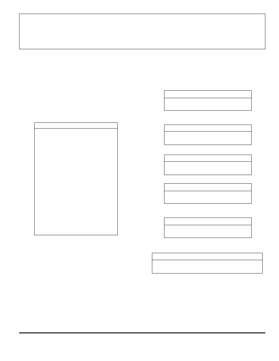
FUNCTIONAL BLOCK DIAGRAM
Copyright � 2000, Allegro MicroSystems, Inc.
CONTROL
LOGIC
REGULATOR
UVLO AND
FAULT
DETECT
OUT
1A
SENSE
1
GATE
DRIVE
CHARGE PUMP
V
REG
CP1
CP2
V
CP
V
BB1
BANDGAP
OSC
SERIAL
PORT
CLOCK
DATA
STROBE
OUT
1B
0.22
�F
+
-
V
DD
PHASE 1/2
SYNC. RECT. MODE
SYNC. RECT. DISABLE
MODE 1/2
0.22
�F
0.22
�F
REF
OUT
2A
V
BB2
OUT
2B
SENSE
2
PROGRAMMABLE
PWM TIMER
FIXED-OFF
BLANK
MIXED DECAY
PROGRAMMABLE
PWM TIMER
FIXED-OFF
BLANK
MIXED DECAY
6-BIT
LINEAR
DAC
+
-
SENSE
1
V
CP
2 V
2 V
GROUND
MUX
OSCILATOR
OSC SELECT/
DIVIDER
BUFFER
0.1
�F
SLEEP
DMOS H-BRIDGE
DMOS H-BRIDGE
15
14
24
11
12
10
23
13
17
21
16
20
8
4
9
5
1
3
2
22
6
7
18 19
LOAD
SUPPLY
LOGIC
SUPPLY
0.1
�F
Dwg. FP-050-1
6
6
6-BIT
LINEAR
DAC

3973
DUAL DMOS FULL-BRIDGE
MICROSTEPPING PWM MOTOR DRIVER
www.allegromicro.com
3
ELECTRICAL CHARACTERISTICS at T
A
= +25
�
C, V
BB
= 35 V, V
DD
= 5.0 V, V
S
= 0.5 V,
f
PWM
< 50 kHz (unless otherwise noted).
Limits
Characteristic
Symbol
Test Conditions
Min.
Typ.
Max.
Units
Load Supply Voltage Range
V
BB
Operating
15
--
35
V
During sleep mode
0
--
35
V
Logic Supply Voltage Range
V
DD
Operating
4.5
5.0
5.5
V
Load Supply Current
I
BB
f
PWM
< 50 kHz
--
--
8.0
mA
Operating, outputs disabled
--
--
6.0
mA
Sleep or idle mode
--
--
20
�A
Logic Supply Current
I
DD
f
PWM
< 50 kHz
--
--
12
mA
Outputs off
--
--
10
mA
Idle mode (D0 = 1, D18 = 0)
--
--
1.5
mA
Sleep mode
--
--
100
�A
Output Drivers
Output Leakage Current
I
DSS
V
OUT
= V
BB
--
<1.0
50
�A
V
OUT
= 0 V
--
<-1.0
-50
�A
Output On Resistance
r
DS(on)
Source driver, I
OUT
= �1.0 A
--
0.54
0.60
Sink driver, I
OUT
= 1.0 A
--
0.54
0.60
Body Diode Forward Voltage
V
F
Source diode, I
F
= 1.0 A
--
--
1.2
V
Sink diode, I
F
= 1.0 A
--
--
1.2
V
Control Logic
Logic Input Voltage
V
IN(1)
2.0
--
--
V
V
IN(0)
--
--
0.8
V
Logic Input Current
I
IN(1)
V
IN
= 2.0 V
--
<1.0
20
�A
I
IN(0)
V
IN
= 0.8 V
--
<-2.0
-20
�A
OSC Input Frequency Range
f
OSC
Divide by one
2.5
--
6.0
MHz
(D0 =1, D13 = 0, D14 = 1)
OSC Input Duty Cycle
--
40
--
60
%
Input Hysterisis
V
IN
0.20
--
0.40
V
continued next page ...

3973
DUAL DMOS FULL-BRIDGE
MICROSTEPPING PWM MOTOR DRIVER
115 Northeast Cutoff, Box 15036
Worcester, Massachusetts 01615-0036 (508) 853-5000
4
ELECTRICAL CHARACTERISTICS at T
A
= +25
�
C, V
BB
= 35 V, V
DD
= 5.0 V, V
S
= 0.5 V,
f
PWM
< 50 kHz (unless otherwise noted).
Limits
Characteristics
Symbol
Test Conditions
Min.
Typ.
Max.
Units
Control Logic (continued)
Internal Oscillator
f
OSC
OSC shorted to ground
3.0
4.0
5.0
MHz
R
OSC
= 51 k
3.4
4.0
4.6
MHz
DAC Accuracy (total error)
E
T
Relative to DAC reference buffer
--
�1/2
--
LSB
output, D0 = 0, D17 = 0
Reference Input Voltage Range
V
REF(EXT)
0.5
--
2.6
V
Reference Buffer Offset
V
OS
--
�10
--
mV
Reference Divider Ratio
V
REF
/V
S
D0 = 0, D18 = 0
--
8.0
--
--
D0 = 0, D18 = 1
--
4.0
--
--
Reference Input Current
I
REF
V
REF
= 2.0 V
--
--
�0.5
�A
Internal Reference Voltage
V
REF(INT)
1.94
2.0
2.06
V
Gain (G
m
) Error (note 3)
E
G
D0 = 0, D17 = 0,
D18 = 0, DAC = 63
--
0
�6
%
D18 = 0, DAC = 31
--
0
�9
%
D18 = 1, DAC = 63
--
0
�6
%
D18 = 1, DAC = 15
--
0
�10
%
Comparator Input Offset Voltage
V
IO
V
REF
= 0 V
--
�5.0
--
mV
Propagation Delay Times
t
pd
50% to 90%:
PWM change to source on
500
800
1200
ns
PWM change to source off
50
150
350
ns
PWM change to sink on
500
800
1200
ns
PWM change to sink off
50
150
350
ns
Crossover Dead Time
t
dt
300
700
900
ns
Thermal Shutdown Temperature
T
J
--
165
--
�C
Thermal Shutdown Hysteresis
T
J
--
15
--
�C
UVLO Enable Threshold
V
UVLO
Increasing V
DD
3.9
4.2
4.45
V
UVLO Hysteresis
V
UVLO
0.05
0.10
--
V
NOTES: 1. Typical Data is for design information only.
2. Negative current is defined as coming out of (sourcing) the specified device terminal.
3. E
G
= [(V
REF
/Range) � V
S
]/(V
REF
/Range).
3973
DUAL DMOS FULL-BRIDGE
MICROSTEPPING PWM MOTOR DRIVER
www.allegromicro.com
5
Serial Interface. The A3973SB/SLB is controlled via a
3-wire (clock, data, strobe) serial port. The programmable
functions allow maximum flexibility in configuring the PWM to
the motor drive requirements. The serial data is written as two
19-bit words: 1 bit to select the word and 18 bits of data. The
serial data is clocked in starting with D18.
Word 0 Bit Assignments
Bit
Function
D0
Word select = 0
D1
Bridge 1, DAC, LSB
D2
Bridge 1, DAC, bit 2
D3
Bridge 1, DAC, bit 3
D4
Bridge 1, DAC, bit 4
D5
Bridge 1, DAC, bit 5
D6
Bridge 1, DAC, MSB
D7
Bridge 2, DAC, LSB
D8
Bridge 2, DAC, bit 2
D9
Bridge 2, DAC, bit 3
D10
Bridge 2, DAC, bit 4
D11
Bridge 2, DAC, bit 5
D12
Bridge 2, DAC, MSB
D13
Bridge 1 phase
D14
Bridge 2 phase
D15
Bridge 1 mode
D16
Bridge 2 mode
D17
REF select
D18
Range select
D1 � D6 Bridge 1 Linear DAC. Six-bit word sets desired
current level for Bridge 1. Setting all six bits to zero disables
Bridge 1, with all drivers off (See current regulation section of
functional description).
D7 � D12 Bridge 2 Linear DAC. Six-bit word sets desired
current level for Bridge 2. Setting all six bits to zero disables
Bridge 2, with all drivers off (See current regulation section of
functional description).
FUNCTIONAL DESCRIPTION
continued next page ...
D13 Bridge 1 Phase. This bit controls the direction of
output current for Load 1.
D13
OUT
1A
OUT
1B
0
L
H
1
H
L
D14 Bridge 2 Phase. This bit controls the direction of
output current for Load 2.
D14
OUT
2A
OUT
2B
0
L
H
1
H
L
D15 Bridge 1 Mode.
D15
Mode
0
Mixed-decay
1
Slow-decay
D16 Bridge 2 Mode.
D16
Mode
0
Mixed-decay
1
Slow-decay
D17 REF Select. This bit determines the reference input for
the 6-bit linear DACs.
D17
Reference Voltage
0
Internal 2 V
1
External (3 V max)
D18 G
m
Range Select. This bit determines the scaling factor
(4 or 8) used.
D18
Divider
Load Current
0
1/8
I
TRIP
= V
DAC
/8R
S
1
1/4
I
TRIP
= V
DAC
/4R
S